

Page 1
p
Preliminary Datasheet
Single/Dual Low Bias Current, Low Voltage, Rail-to-Rail
In
ut/Output CMOS Operational Amplifiers MOS Operational
General Description
The AZV831/AZV832 is single/dual channels
rail-to-rail input and output amplifier, which provides
a wide input common-mode voltage range and output
voltage swing capability for maximum signal swings
in low supply voltage applications. The device is
fully specified to operate from 1.6V to 5.0V single
supply, or ±0.8V and ±2.5V dual supply applications.
It features very low supply current dissipation 70µA
per channel, which is well suitable for today's
low-voltage and/or portable systems.
The AZV831/AZV832 features optimal performance
in very low bias current of 1pA, which enables the IC
to be used for integrators, photodiode amplifiers, and
piezoelectric sensors etc. The device has typical
0.5mV input offset voltage and provides 1MHz
bandwidth.
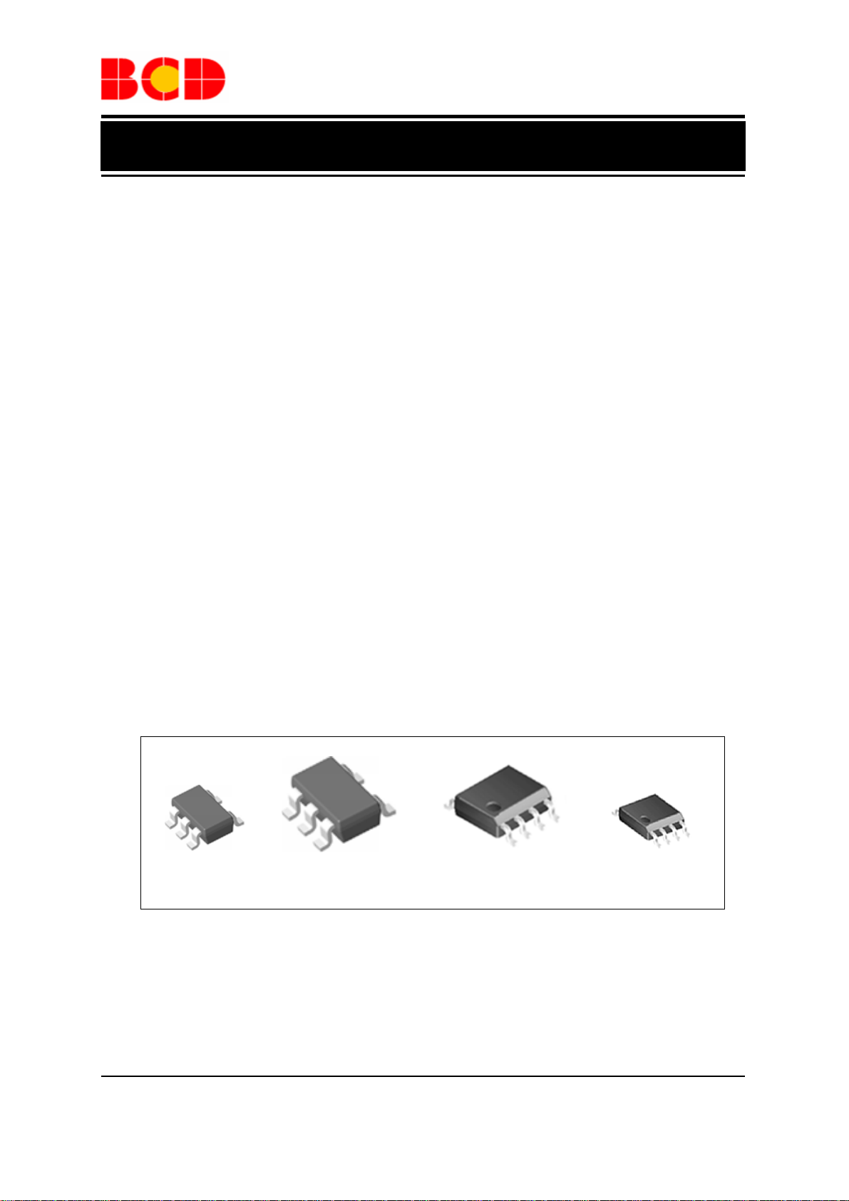
The AZV831/AZV832 adopts the latest packaging
technology to meet the most demanding
space-constraint applications. The AZV831 is
available in standard SOT-23-5 and SC-70-5
packages. The AZV832 is offered in the traditional
MSOP-8 and SOIC-8 packages.
SC-70-5 SOT-23-5 SOIC-8 MSOP-8
Figure 1. Package Types of AZV831/AZV832
Features
• Single Supply Voltage Range: 1.6V to 5.5V
• Ultra-low Input Bias Current: 1pA (Typ.)
• Offset Voltage: 0.5mV (Typ.), 2.5mV (Max.)
• Rail-to-Rail Input
V
: 300mV beyond Rails @ VCC=5V
CM
Rail-to-Rail Output Swing:
10k
1kΩ Load: 25mV from Rail
• Supply Current: 70µA/Amplifier
• Unity Gain Stable
• Slew Rate: 0.45V/µs @ V
• Operation Ambient Temperature Range: -40ºC
Ω Load: 4mV from Rail
Gain Bandwidth Product: 1.0MHz
to 85ºC
Applications
• Sensors
• Photodiode Amplification
• Battery-Powered Instrumentation
• Pulse Blood Oximeter, Glucose Meter
AZV831/2
=5.0V
CC
Jul. 2012 Rev. 1. 0 BCD Semiconductor Manufacturing Limited
1
Page 2
Preliminary Datasheet
Single/Dual Low Bias Current, Low Voltage, Rail-to-Rail
Input/Output CMOS Operational Amplifiers
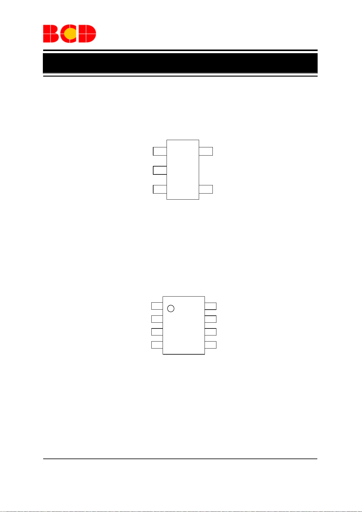
Pin Configuration
KS/K Package
(SC-70-5/SOT-23-5)
OUTPUT VCC
1
5
VEE
2
IN+ IN-
34
AZV831
M/MM Package
(SOIC-8/MSOP-8)
OUTPUT 1 VCC
1
8
IN 1- OUTPUT 2
2
7
IN 1+ IN 2-
3
6
VEE
4
5
IN 2+
AZV832
Figure 2. Pin Configuration of AZV831/2 (Top View)
AZV831/2
Jul. 2012 Rev. 1. 0 BCD Semiconductor Manufacturing Limited
2
Page 3
Preliminary Datasheet
Single/Dual Low Bias Current, Low Voltage, Rail-to-Rail
Input/Output CMOS Operational Amplifiers
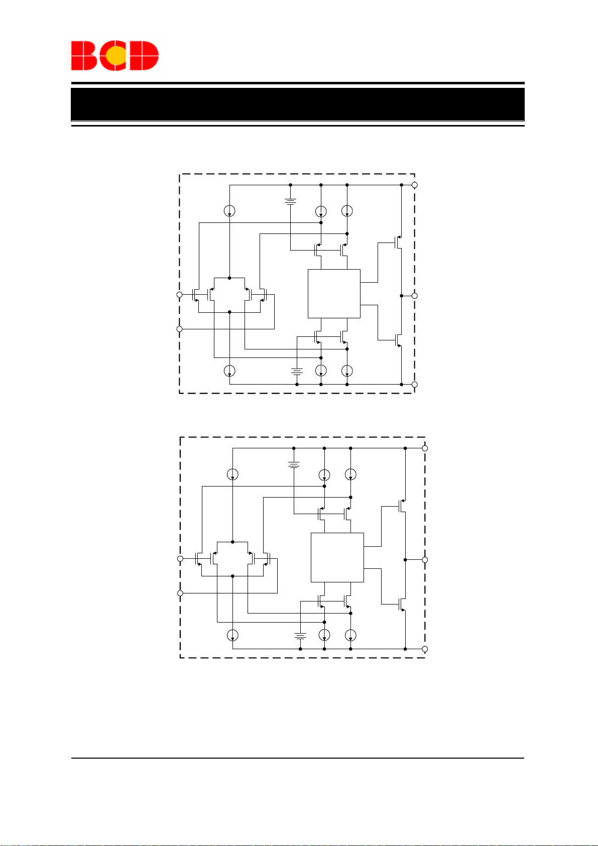
Function Block Diagram
AZV831/2
+
-
5
VCC
4
IN-
IN+
3
Class
AB
Control
1
OUTPUT
+
-
2
VEE
For AZV831
+
-
8
VCC
IN1-/IN2-
IN1+/IN2+
2,6
3,5
Class
AB
Control
1,7
OUTPUT1/
OUTPUT2
+
For AZV832/Amplifier
Figure 3. Functional Block Diagram of AZV831/2
-
4
VEE
Jul. 2012 Rev. 1. 0 BCD Semiconductor Manufacturing Limited
3
Page 4
Preliminary Datasheet
Single/Dual Low Bias Current, Low Voltage, Rail-to-Rail
Input/Output CMOS Operational Amplifiers
Ordering Information
AZV831/2 -
Circuit Type G1: Green
Package Blank: Tube
KS: SC-70-5 (AZV831)
K: SOT-23-5 (AZV831)
M: SOIC-8 (AZV832)
MM: MSOP-8 (AZV832)
TR: Tape & Reel
AZV831/2
Package
SC-70-5
SOT-23-5
SOIC-8
MSOP-8
BCD Semiconductor's Pb-free products, as designated with "G1" suffix in the part number, are RoHS compliant
and green.
Temperature
Range
-40 to 85°C
-40 to 85°C
-40 to 85°C
-40 to 85°C
Part Number Marking ID
AZV831KSTR-G1 L3 Tape & Reel
AZV831KTR-G1 G4D Tape & Reel
AZV832M-G1 832M-G1 Tube
AZV832MTR-G1 832M-G1
AZV832MM-G1 832MM-G1
AZV832MMTR-G1 832MM-G1
Packing
Type
Tape & Reel
Tube
Tape & Reel
Jul. 2012 Rev. 1. 0 BCD Semiconductor Manufacturing Limited
4
Page 5
Preliminary Datasheet
Single/Dual Low Bias Current, Low Voltage, Rail-to-Rail
AZV831/2
Input/Output CMOS Operational Amplifiers
Absolute Maximum Ratings (Note 1)
Parameter Symbol Value Unit
Power Supply Voltage VCC 6.0 V
Differential Input Voltage VID 6.0 V
Input Voltage VIN -0.3 to VCC+0.5 V
Operating Junction Temperature TJ 150 ºC
SC-70-5 270
Thermal Resistance
(Junction to Ambient)
θ
JA
SOT-23-5 220
SOIC-8 150
MSOP-8 200
ºC /W
Storage Temperature Range T
Lead Temperature (Soldering,10 Seconds) T
ESD (Human Body Model) 4000 V
ESD (Machine Model) 300 V
Note 1: Stresses greater than those listed under “Absolute Maximum Ratings” may cause permanent damage to
the device. These are stress ratings only, and functional operation of the device at these or any other conditions
beyond those indicated under “Recommended Operating Conditions” is not implied. Exposure to “Absolute
Maximum Ratings” for extended periods may affect device reliability.
-65 to 150 ºC
STG
260 ºC
LEAD
Recommended Operating Conditions
Parameter Symbol Min Max Unit
Supply Voltage VCC 1.6 5.5 V
Operation Ambient Temperature
Range
-40 85 ºC
T
A
Jul. 2012 Rev. 1. 0 BCD Semiconductor Manufacturing Limited
5
Page 6

Preliminary Datasheet
Single/Dual Low Bias Current, Low Voltage, Rail-to-Rail
AZV831/2
Input/Output CMOS Operational Amplifiers
1.6V DC Electrical Characteristics
VCC=1.6V, VEE=0, V
OUT=VCC
Parameter Symbol Conditions Min Typ Max Unit
Input Offset Voltage VOS 0.5 2.5 mV
Input Bias Current IB 1.0 pA
Input Offset Current IOS 1.0 pA
Input Common-mode Voltage Range VCM -0.2 1.8 V
Common-mode Rejection Ratio CMRR VCM=-0.2V to 1.8V 55 75 dB
Large Signal Voltage Gain GV
Input Offset Voltage Drift ∆VOS/∆T 2.0
/2, VCM=VCC/2, TA=25°C, unless otherwise noted.
=10kΩ to VCC/2,
R
L
=0.2V to 1.4V
V
OUT
90 110 dB
µV/ °C
RL=1kΩ to VCC/2 30 50
Output Voltage Swing from Rail VOL/V
OH
mV
RL=10kΩ to VCC/2 3 15
Sink I
Output Current
Source I
Closed-loop Output Impedance Z
Power Supply Rejection Ratio PSRR VCC=1.6V to 5.0V
Supply Current (Per Amplifier) ICC V
V
SINK
SOURCE
OUT
OUT=VCC
V
OUT
f=10kHz, AV=1 9 Ω
OUT=VCC
8 10
=0V 5 8.5
66 80 dB
/2, I
=0 70 90 µA
OUT
mA
1.6V AC Electrical Characteristics
=1.6V, VEE=0, V
V
CC
OUT=VCC
/2, VCM=VCC/2, TA=25°C, unless otherwise noted.
Parameter Symbol Conditions Min Typ Max Unit
Gain Bandwidth Product GBP RL=100kΩ 1.0 MHz
Slew Rate (Note 2) SR
Phase Margin φM RL=100kΩ 67 Degrees
Total Harmonic Distortion+Noise THD+N
Voltage Noise Density en f=1kHz 27
Note 2: Number specified is the positive slew rate.
.
1V Step,
=100pF, RL=10kΩ
C
L
f=1kHz, A
=10kΩ, CL=100pF
R
L
=1, VIN=1Vpp
V
0.32 V/µs
-70 dB
HznV/
Jul. 2012 Rev. 1. 0 BCD Semiconductor Manufacturing Limited
6
Page 7
Preliminary Datasheet
Single/Dual Low Bias Current, Low Voltage, Rail-to-Rail
AZV831/2
Input/Output CMOS Operational Amplifiers
1.8V DC Electrical Characteristics
VCC=1.8V, VEE=0, V
OUT=VCC
Parameter Symbol Conditions Min Typ Max Unit
Input Offset Voltage VOS 0.5 2.5 mV
Input Bias Current IB 1.0 pA
Input Offset Current IOS 1.0 pA
Input Common-mode Voltage Range VCM -0.2 2.0 V
Common-mode Rejection Ratio CMRR VCM=-0.2V to 2.0V 55 75 dB
Large Signal Voltage Gain GV
Input Offset Voltage Drift ∆VOS/∆T 2.0
/2, VCM=VCC/2, TA=25°C, unless otherwise noted.
=10kΩ to VCC/2,
R
L
=0.2V to 1.6V
V
OUT
90 112 dB
µV/ °C
RL=1kΩ to VCC/2 25 50
Output Voltage Swing from Rail VOL/V
OH
mV
RL=10kΩ to VCC/2 3 15
Sink I
Output Current
Source I
Closed-loop Output Impedance Z
Power Supply Rejection Ratio PSRR VCC=1.6V to 5.0V
Supply Current (Per Amplifier) ICC V
V
SINK
SOURCE
OUT
OUT=VCC
V
OUT
f=10kHz 9 Ω
OUT=VCC
12 16
=0V 10 14
66 80 dB
/2, I
=0 70 90 µA
OUT
mA
1.8V AC Electrical Characteristics
=1.8V, VEE=0, V
V
CC
OUT=VCC
/2, VCM=VCC/2, TA=25°C, unless otherwise noted.
Parameter Symbol Conditions Min Typ Max Unit
Gain Bandwidth Product GBP RL=100kΩ 1.0 MHz
Slew Rate (Note 2) SR
1V Step,
=100pF, RL=10kΩ
C
L
0.34 V/µs
Phase Margin φM RL=100kΩ 67 Degrees
Total Harmonic Distortion+Noise THD+N
f=1kHz, A
=10kΩ, CL=100pF
R
L
Voltage Noise Density en f=1kHz 27
=1, VIN=1Vpp
V
-70 dB
HznV/
Note 2: Number specified is the positive slew rate.
Jul. 2012 Rev. 1. 0 BCD Semiconductor Manufacturing Limited
7
Page 8

Preliminary Datasheet
Single/Dual Low Bias Current, Low Voltage, Rail-to-Rail
AZV831/2
Input/Output CMOS Operational Amplifiers
3.0V DC Electrical Characteristics
VCC=3.0V, VEE=0, V
OUT=VCC
Parameter Symbol Conditions Min Typ Max Unit
Input Offset Voltage VOS 0.5 2.5 mV
Input Bias Current IB 1.0 pA
Input Offset Current IOS 1.0 pA
Input Common-mode Voltage Range VCM -0.3 3.3 V
Common-mode Rejection Ratio CMRR
Large Signal Voltage Gain GV
Input Offset Voltage Drift ∆VOS/∆T 2.0
/2, VCM=VCC/2, TA=25°C, unless otherwise noted.
V
=-0.3V to 1.8V 62 80
CM
VCM=-0.3V to 3.3V 58 75
R
=1kΩ to VCC/2 ,
L
=0.2V to 2.8V
V
OUT
RL=10kΩ to VCC/2,
=0.1V to 2.9V
V
OUT
dB
90 110
dB
95 115
µV/ °C
RL=1kΩ to VCC/2 20 50
Output Voltage Swing from Rail VOL/V
OH
mV
RL=10kΩ to VCC/2 3 15
Sink I
Output Current
Source I
Closed-loop Output Impedance Z
Power Supply Rejection Ratio PSRR VCC=1.6V to 5.0V
Supply Current (Per Amplifier) ICC V
V
SINK
SOURCE
OUT
OUT=VCC
V
OUT
f=10kHz 9 Ω
OUT=VCC
50 60
=0V 50 65
66 80 dB
/2, I
=0 70 90 µA
OUT
mA
3.0V AC Electrical Characteristics
V
=3.0V, VEE=0, V
CC
OUT=VCC
/2, VCM=VCC/2, TA=25°C, unless otherwise noted.
Parameter Symbol Conditions Min Typ Max Unit
Gain Bandwidth Product GBP RL=100kΩ 1.0 MHz
Slew Rate (Note 2) SR
Phase Margin φM RL=100kΩ 67 Degrees
Total Harmonic Distortion+Noise THD+N
Voltage Noise Density en f=1kHz 27
Note 2: Number specified is the positive slew rate.
G=1, 2V Step,
=100pF, RL=10kΩ
C
L
f=1kHz, G=1, V
=10kΩ, CL=100pF
R
L
=1Vpp
IN
0.40 V/µs
-70 dB
HznV/
Jul. 2012 Rev. 1. 0 BCD Semiconductor Manufacturing Limited
8
Page 9

Preliminary Datasheet
Single/Dual Low Bias Current, Low Voltage, Rail-to-Rail
AZV831/2
Input/Output CMOS Operational Amplifiers
5.0V DC Electrical Characteristics
=5.0V, VEE=0, V
V
CC
OUT=VCC
Parameter Symbol Conditions Min Typ Max Unit
Input Offset Voltage VOS 0.5 2.5 mV
Input Bias Current IB 1.0 pA
Input Offset Current IOS 1.0 pA
Input Common-mode Voltage Range VCM -0.3 5.3 V
Common-mode Rejection Ratio CMRR
Large Signal Voltage Gain GV
Input Offset Voltage Drift ∆VOS/∆T 2.0
/2, VCM=VCC/2, T
=25°C, unless otherwise noted.
A
V
=-0.3V to 3.8V 70 85
CM
VCM=-0.3V to 5.3V 65 90
R
=1kΩ to VCC/2,
L
=0.2V to 4.8V
V
OUT
RL=10kΩ to VCC/2,
=0.05V to 4.95V
V
OUT
80 92
85 98
dB
dB
µV/°C
RL=1kΩ to VCC/2 25 50
Output Voltage Swing from Rail VOL/V
OH
mV
RL=10kΩ to VCC/2 4 15
Sink I
Output Current
Source I
SINK
SOURCE
V
OUT=VCC
V
OUT
100 150
mA
=0V 110 185
Closed-loop Output Impedance f=1kHz, AV=1 9 Ω
Power Supply Rejection Ratio PSRR VCC=1.6V to 5.0V
Supply Current (Per Amplifier) ICC V
OUT=VCC
/2, I
OUT
=0 70 90 µA
66 80 dB
5V AC Electrical Characteristics
VCC=5.0V, VEE=0, V
OUT=VCC
Parameter Symbol Conditions Min Typ Max Unit
Gain Bandwidth Product GBP RL=100kΩ 1.0 MHz
Slew Rate (Note 2) SR
Phase Margin φM RL=100kΩ 67 Degrees
THD+N THD+N
Voltage Noise Density en f=1kHz 27
Note 2: Number specified is the positive slew rate.
Jul. 2012 Rev. 1. 0 BCD Semiconductor Manufacturing Limited
/2, VCM=VCC/2, TA=25°C, unless otherwise noted.
2V Step,
=100pF, RL=10kΩ
C
L
f=1kHz, A
=10kΩ,CL=100pF
R
L
=1, VIN=1VPP
V
9
0.45 V/µs
-70 dB
HznV/
Page 10

Preliminary Datasheet
Single/Dual Low Bias Current, Low Voltage, Rail-to-Rail
Input/Output CMOS Operational Amplifiers
Typical Performance Characteristics
260
240
220
200
180
160
140
Supply Current (µA)
120
100
80
-40-20 0 20406080100120
1
0
-1
-2
-3
-4
Input Offset Voltage (mV)
-5
-6
-0.5 0.0 0.5 1.0 1.5 2.0
No Load
V
=1/2V
OUT
CC
VCC=1.8V
VCC=1.6V
Temperature (OC)
Dual Amplifiers
VCC=5.0V
VCC=3.0V
Figure 4. Supply Current vs. Temperature Figure 5. Supply Current vs. Supply Voltage
VCC=1.6V
TA=-40oC
TA=25oC
Input Common Mode Voltage (V)
TA=85oC
Figure 6. Input Offset Voltage vs. Figure 7. Input Offset Voltage vs.
Input Common Mode Voltage Input Common Mode Voltage
250
200
150
100
Supply Current (µA)
TA=25OC
TA=-40OC
TA=85OC
50
0
1.5 2.0 2.5 3.0 3.5 4.0 4.5 5.0 5.5
Supply Voltage (V)
1
VCC=1.8V
0
-1
-2
-3
-4
Input Offset Voltage (mV)
-5
-6
-0.5 0.0 0.5 1.0 1.5 2.0 2.5
Input Common Mode Voltage (V)
AZV831/2
Dual Amplifiers
/2
V
OUT=VCC
=0mA
I
OUT
TA=-40oC
TA=25oC
TA=85oC
Jul. 2012 Rev. 1. 0 BCD Semiconductor Manufacturing Limited
10
Page 11

Preliminary Datasheet
Single/Dual Low Bias Current, Low Voltage, Rail-to-Rail
AZV831/2
Input/Output CMOS Operational Amplifiers
Typical Performance Characteristics (Continued)
1
Input Offset Voltage (mV)
VCC=3.0V
0
-1
-2
-3
-4
-5
-6
01234
Input Common Mode Voltage (V)
TA=-40oC
TA=25oC
TA=85oC
Figure 8. Input Offset Voltage vs. Figure 9. Input Offset Voltage vs.
Input Common Mode Voltage Input Common Mode Voltage
1000
VCC=1.6V, VEE=0V
100
10
Output Voltage to Supply Rail (mV)
1
0.1 1 10
Output Current (mA)
Sink Current
Source Current
Figure 10. Output Voltage vs. Output Current Figure 11. Output Voltage vs. Output Current
4
VCC=5.0V
2
0
-2
-4
Input Offset Voltage (mV)
-6
0123456
Input Common Mode Voltage (V)
TA=-40oC
TA=25oC
TA=85oC
1000
VCC=1.8V, VEE=0V
100
10
Sink Current
Output Voltage to Supply Rail (mV)
1
0.1 1 10
Output Current (mA)
Source Current
Jul. 2012 Rev. 1. 0 BCD Semiconductor Manufacturing Limited
11
Page 12

Preliminary Datasheet
Single/Dual Low Bias Current, Low Voltage, Rail-to-Rail
AZV831/2
Input/Output CMOS Operational Amplifiers
Typical Performance Characteristics (Continued)
1000
VCC=3.0V, VEE=0V
10000
VCC=5.0V, VEE=0V
1000
100
100
10
Output Voltage to Supply Rail (mV)
1
0.01 0.1 1 10
Output Current (mA)
Sink Current
Source Current
10
Output Voltage to Supply Rail (mV)
1
0.01 0.1 1 10 100
Output Current (mA)
Sink Current
Source Current
Figure 12. Output Voltage vs. Output Current Figure 13. Output Voltage vs. Output Current
160
VEE=0V
140
120
100
80
60
40
20
Output Short Circuit Current (Sink) (mA)
short to V
V
OUT
0
-40-200 20406080100
CC
Temperature (oC)
VCC=1.6V
VCC=1.8V
VCC=3.0V
VCC=5.0V
Figure 14. Output Short Circuit Current vs. Temperature Figure 15. Output Short Circuit Current vs. Temperature
200
VEE=0V
180
V
short to V
OUT
160
140
120
100
80
60
40
20
Output Short Circuit Current (Source) (mA)
0
-40-200 20406080100
EE
VCC=1.6V
VCC=1.8V
VCC=3.0V
VCC=5.0V
Temperature (oC)
Jul. 2012 Rev. 1. 0 BCD Semiconductor Manufacturing Limited
12
Page 13

Preliminary Datasheet
Single/Dual Low Bias Current, Low Voltage, Rail-to-Rail
AZV831/2
Input/Output CMOS Operational Amplifiers
Typical Performance Characteristics (Continued)
120
100
VEE=0V
short to V
V
OUT
80
60
CC
160
140
120
100
VEE=0V
short to V
V
OUT
80
EE
40
20
Output Short Circuit Current (Sink) (mA)
0
12345
Figure 16. Output Short Circuit Current Figure 17. Output Short Circuit Current
vs. Supply Voltage vs. Supply Voltage
4.0
3.5
RL=10kΩ
3.0
2.5
2.0
Output Voltage to Supply Rail (mV)
1.5
0.81.01.21.41.61.82.02.22.42.6
Figure 18. Output Voltage Swing vs. Supply Voltage Figure 19. Output Voltage Swing vs. Supply Voltage
Supply Voltage (V)
Positive Swing
Negative Swing
Dual Supply Voltage (V)
60
40
20
Output Short Circuit Current (Source) (mA)
0
12345
Supply Voltage (V)
27
26
25
24
23
22
21
Output Voltage to Supply Rail (mV)
20
0.8 1.0 1.2 1.4 1.6 1.8 2.0 2.2 2.4 2.6
RL=1kΩ
Positive Swing
Negative Swing
Dual Supply Voltage (V)
Jul. 2012 Rev. 1. 0 BCD Semiconductor Manufacturing Limited
13
Page 14

Preliminary Datasheet
Single/Dual Low Bias Current, Low Voltage, Rail-to-Rail
AZV831/2
Input/Output CMOS Operational Amplifiers
Typical Performance Characteristics (Continued)
48
44
40
36
32
Positive Swing
28
24
20
16
Output Voltage to Supply Rail (mV)
12
-40-20 0 20406080100
RL=1kΩ
Temperature (oC)
VCC=0.8V,VEE=-0.8V
VCC=2.5V,VEE=-2.5V
VCC=0.8V,VEE=-0.8V
VCC=2.5V,VEE=-2.5V
Negative Swing
10
9
8
7
6
5
4
3
2
1
Output Voltage to Supply Rail (mV)
0
-40 -20 0 20 40 60 80 100
RL=10kΩ
Negative Swing
Temperature (oC)
VCC=0.9V,VEE=-0.9V
VCC=1.5V,VEE=-1.5V
VCC=0.9V,VEE=-0.9V
VCC=1.5V,VEE=-1.5V
Positive Swing
Figure 20. Output Voltage Swing vs. Temperature Figure 21. Output Voltage Swing vs. Temperature
70
60
50
40
30
20
10
Open Loop Gain (dB)
0
-10
-20
RL=100kΩ
RL=10kΩ
RL=1kΩ
RL=8Ω
VCC=0.8V, VEE=-0.8V
10k 100k 1M
Frequency (Hz)
Figure 22. Gain and Phase vs. Frequency Figure 23. Gain and Phase vs. Frequency
with Resistive Load with Capacitive Load
100
90
80
70
60
50
40
30
20
10
Phase Margin (Degree)
70
60
50
40
30
20
10
Open Loop Gain (dB)
-10
-20
CL=100pF
CL=200pF
0
CL=300pF
VCC=0.8V, VEE=-0.8V
R
=100kΩ
L
10k 100k 1M
Frequency (Hz)
100
90
80
70
60
50
40
30
20
10
Phase Margin (Degree)
Jul. 2012 Rev. 1. 0 BCD Semiconductor Manufacturing Limited
14
Page 15

Preliminary Datasheet
Single/Dual Low Bias Current, Low Voltage, Rail-to-Rail
AZV831/2
Input/Output CMOS Operational Amplifiers
Typical Performance Characteristics (Continued)
70
60
50
40
30
20
10
Open Loop Gain (dB)
0
-10
-20
CL=100pF
CL=200pF
CL=300pF
VCC=0.8V, VEE=-0.8V
R
=10kΩ
L
10k 100k 1M
Frequency (Hz)
Figure 24. Gain and Phase vs. Frequency Figure 25. Gain and Phase vs. Frequency
with Capacitive Load with Resistive Load
70
60
50
40
30
20
10
Open Loop Gain (dB)
0
-10
-20
CL=100pF
CL=200pF
CL=300pF
VCC=0.9V, VEE=-0.9V
R
=100kΩ
L
10k 100k 1M
Frequency (Hz)
Figure 26. Gain and Phase vs. Frequency Figure 27. Gain and Phase vs. Frequency
with Capacitive Load with Capacitive Load
100
90
80
70
60
50
40
30
20
10
100
90
80
70
60
50
40
30
20
10
Phase Margin (Degree)
Phase Margin (Degree)
Open Loop Gain (dB)
-10
-20
70
60
50
40
30
20
10
0
Open Loop Gain (dB)
-10
-20
RL=100kΩ
RL=10kΩ
RL=1kΩ
RL=8Ω
VCC=0.9V, VEE=-0.9V
10k 100k 1M
Frequency (Hz)
70
60
50
40
30
20
10
0
CL=100pF
CL=200pF
CL=300pF
VCC=0.9V, VEE=-0.9V
R
=10kΩ
L
10k 100k 1M
Frequency (Hz)
100
90
80
70
60
50
40
30
20
10
100
90
80
70
60
50
40
30
20
10
Jul. 2012 Rev. 1. 0 BCD Semiconductor Manufacturing Limited
15
Phase Margin (Degree)
Phase Margin (Degree)
Page 16

Preliminary Datasheet
Single/Dual Low Bias Current, Low Voltage, Rail-to-Rail
AZV831/2
Input/Output CMOS Operational Amplifiers
Typical Performance Characteristics (Continued)
70
60
50
40
30
20
Open Loop Gain (dB)
-10
-20
10
0
RL=100kΩ
RL=10kΩ
RL=1kΩ
RL=8Ω
VCC=1.5V, VEE=-1.5V
10k 100k 1M
Frequency (Hz)
Figure 28. Gain and Phase vs. Frequency Figure 29. Gain and Phase vs. Frequency
with Resistive Load with Capacitive Load
70
60
50
40
30
20
10
Open Loop Gain (dB)
0
-10
-20
CL=100pF
CL=200pF
CL=300pF
VCC=1.5V, VEE=-1.5V
R
=10kΩ
L
10k 100k 1M
Frequency (Hz)
Figure 30. Gain and Phase vs. Frequency Figure 31. Gain and Phase vs. Frequency
with Capacitive Load with Resistive Load
100
90
80
70
60
50
40
30
20
10
100
90
80
70
60
50
40
30
20
10
Phase Margin (Degree)
Phase Margin (Degree)
70
60
50
40
30
20
10
Open Loop Gain (dB)
0
-10
-20
70
60
50
40
30
20
10
Open Loop Gain (dB)
0
-10
-20
CL=100pF
CL=200pF
CL=300pF
VCC=1.5V, VEE=-1.5V
R
=100kΩ
L
10k 100k 1M
Frequency (Hz)
RL=100kΩ
RL=10kΩ
RL=1kΩ
RL=8Ω
VCC=2.5V, VEE=-2.5V
10k 100k 1M
Frequency (Hz)
100
90
80
70
60
50
40
30
20
10
100
90
80
70
60
50
40
30
20
10
Jul. 2012 Rev. 1. 0 BCD Semiconductor Manufacturing Limited
16
Phase Margin (Degree)
Phase Margin (Degree)
Page 17

Preliminary Datasheet
Single/Dual Low Bias Current, Low Voltage, Rail-to-Rail
AZV831/2
Input/Output CMOS Operational Amplifiers
Typical Performance Characteristics (Continued)
70
60
50
40
30
20
10
Open Loop Gain (dB)
0
-10
-20
CL=100pF
CL=200pF
CL=300pF
VCC=2.5V, VEE=-2.5V
R
=100kΩ
L
10k 100k 1M
Frequency (Hz)
Figure 32. Gain and Phase vs. Frequency Figure 33. Gain and Phase vs. Frequency
with Capacitive Load with Capacitive Load
1000
100
VCC=1.6V to 5V
V
=0V
EE
10
Output Impedance (Ω)
1
100 1k 10k 100k
Frequency (Hz)
Figure 34. Output Impedance vs. Frequency Figure 35. THD+N vs. Output Voltage
AV=1
AV=10
AV=100
100
90
80
70
60
50
40
30
20
10
Phase Margin (Degree)
70
60
50
40
30
20
10
Open Loop Gain (dB)
-10
-20
0
CL=100pF
CL=200pF
CL=300pF
VCC=2.5V, VEE=-2.5V
R
=10kΩ
L
10k 100k 1M
Frequency (Hz)
10
1
0.1
THD+N (%)
0.01
1E-3
0.01 0.1 1
AV=1, RL=10kΩ, CL=100pF
VCC=0.8V,VEE=-0.8V
VCC=0.9V,VEE=-0.9V
VCC=1.5V,VEE=-1.5V
VCC=2.5V,VEE=-2.5V
Output Voltage (V)
100
90
80
70
60
50
40
30
20
10
Phase Margin (Degree)
Jul. 2012 Rev. 1. 0 BCD Semiconductor Manufacturing Limited
17
Page 18

Preliminary Datasheet
Single/Dual Low Bias Current, Low Voltage, Rail-to-Rail
AZV831/2
Input/Output CMOS Operational Amplifiers
Typical Performance Characteristics (Continued)
1
Bandwidth<10Hz to 22kHz
0.1
VCC=0.8V, VEE=-0.8V
VCC=0.9V, VEE=-0.9V
VCC=1.5V, VEE=-1.5V
VCC=2.5V, VEE=-2.5V
VCC=5.0V, VEE=0V, AV=1
100n
THD+N (%)
0.01
1E-3
V
=100mV
OUT
100 1k 10k
Figure 36. THD+N vs. Frequency Figure 37. Input Voltage Noise Density
, AV=1, RL=10kΩ, CL=100pF
RMS
Frequency (Hz)
Input Voltage Noise (V/ Hz)
10n
100 1k 10k
Frequency (Hz)
V
IN VIN
50mV/div 50mV/div
V
=1.6V
CC
VEE=0V
=1.8V
V
CC
V
=0V
EE
V
OUT VOUT
50mV/div 50mV/div
CL=100pF, RL=100kΩ, AV=1
C
=100pF, RL=100kΩ, AV=1
L
Time (2µs/div) Time (2µs/div)
Figure 38. Small Signal Pulse Response Figure 39. Small Signal Pulse Response
Jul. 2012 Rev. 1. 0 BCD Semiconductor Manufacturing Limited
18
Page 19

Preliminary Datasheet
Single/Dual Low Bias Current, Low Voltage, Rail-to-Rail
Input/Output CMOS Operational Amplifiers
Typical Performance Characteristics (Continued)
V
IN VIN
50mV/div 50mV/div
VCC=3.0V
V
=0V
EE
V
OUT VOUT
50mV/div 50mV/div
CL=100pF, RL=100kΩ, AV=1
=100pF, RL=100kΩ, AV=1
C
L
Time (2µs/div) Time (2µs/div)
Figure 40. Small Signal Pulse Response Figure 41. Small Signal Pulse Response
V
500mV/div 500mV/div
IN VIN
VCC=1.6V
=0V
V
EE
V
OUT VOUT
500mV/div 500mV/div
C
=200pF, RL=100kΩ, AV=1
L
C
=200pF, RL=100kΩ, AV=1
L
Time (10µs/div) Time (10µs/div)
Figure 42. Large Signal Pulse Response Figure 43. Large Signal Pulse Response
AZV831/2
VCC=5.0V
=0V
V
EE
VCC=1.8V
V
=0V
EE
Jul. 2012 Rev. 1. 0 BCD Semiconductor Manufacturing Limited
19
Page 20

Preliminary Datasheet
Single/Dual Low Bias Current, Low Voltage, Rail-to-Rail
Input/Output CMOS Operational Amplifiers
Typical Performance Characteristics (Continued)
=3.0V
V
V
IN VIN
1V/div 2V/div
CC
V
=0V
EE
V
OUT VOUT
1V/div 2V/div
CL=200pF, RL=100kΩ, AV=1
C
=200pF, RL=100kΩ, AV=1
L
Time (10µs/div) Time (10µs/div)
Figure 44. Large Signal Pulse Response Figure 45. Large Signal Pulse Response
AZV831/2
=5.0V
V
CC
=0V
V
EE
V
500mV/div 500mV/div
IN VIN
V
V
=1.6V
CC
=0V
EE
V
OUT VOUT
500mV/div 500mV/div
C
=200pF, RL=10kΩ, AV=1
L
Time (10µs/div) Time (10µs/div)
Figure 46. Large Signal Pulse Response Figure 47. Large Signal Pulse Response
V
=1.8V
CC
V
=0V
EE
CL=200pF, RL=10kΩ, AV=1
Jul. 2012 Rev. 1. 0 BCD Semiconductor Manufacturing Limited
20
Page 21

Preliminary Datasheet
Single/Dual Low Bias Current, Low Voltage, Rail-to-Rail
Input/Output CMOS Operational Amplifiers
Typical Performance Characteristics (Continued)
V
IN VIN
1V/div 2V/div
VCC=3.0V
=0V
V
EE
V
OUT VOUT
1V/div 2V/div
=200pF, RL=10kΩ, AV=1
C
L
=200pF, RL=10kΩ, AV=1
C
L
Time (10µs/div) Time (10µs/div)
Figure 48. Large Signal Pulse Response Figure 49. Large Signal Pulse Response
AZV831/2
V
=5.0V
CC
V
=0V
EE
V
IN VIN
1V/div 50mV/div
V
OUT VOUT
1V/div 1V/div
V
IN
V
=2.5V
CC
=-2.5V
V
EE
V
OUT
f=1kHz, RL=10kΩ, VIN=6V
PP, AV
=1
Time (200µs/div) Time (20µs/div)
Figure 50. No Phase Reversal Figure 51. Overload Recovery Time
VCC=2.5V
V
=-2.5V
EE
C
=100pF, RL=100kΩ, AV=-50
L
V
=0 to -100mV
IN
Jul. 2012 Rev. 1. 0 BCD Semiconductor Manufacturing Limited
21
Page 22

Preliminary Datasheet
Single/Dual Low Bias Current, Low Voltage, Rail-to-Rail
Input/Output CMOS Operational Amplifiers
Typical Performance Characteristics (Continued)
V
50mV/div
IN
VCC=2.5V
V
=-2.5V
EE
V
OUT
1V/div
CL=100pF, RL=100kΩ, AV =-50,
=0 to -100mV
V
Time (20µs/div)
Figure 52. Overload Recovery Time
AZV831/2
Jul. 2012 Rev. 1. 0 BCD Semiconductor Manufacturing Limited
22
Page 23

Preliminary Datasheet
Single/Dual Low Bias Current, Low Voltage, Rail-to-Rail
AZV831/2
Input/Output CMOS Operational Amplifiers
Mechanical Dimensions
SC-70-5 Unit: mm(inch)
2.150(0.085)
2.450(0.096)
2.000(0.079)
2.200(0.087)
0.150(0.006)
0.350(0.014)
0.260(0.010)
0.460(0.018)
1.150(0.045)
0°
8°
0.200(0.008)
1.350(0.053)
0.525(0.021)REF
0.650(0.026)TYP
1.200(0.047)
1.400(0.055)
0.000(0.000)
0.100(0.004)
0.080(0.003)
0.150(0.006)
0.900(0.035)
1.000(0.039)
0.900(0.035)
1.100(0.043)
Jul. 2012 Rev. 1. 0 BCD Semiconductor Manufacturing Limited
23
Page 24

Preliminary Datasheet
Single/Dual Low Bias Current, Low Voltage, Rail-to-Rail
AZV831/2
Input/Output CMOS Operational Amplifiers
Mechanical Dimensions (Continued)
SOT-23-5 Unit: mm(inch)
2.820(0.111)
3.020(0.119)
0.100(0.004)
0.200(0.008)
)
)
4
)
)
)
4
6
0
1
1
1
.
.
0
0
(
(
0
0
5
5
6
9
.
.
2
2
)
7
9
6
5
0
0
.
.
0
0
(
(
0
0
0
0
5
7
.
.
1
1
0.200(0.008)
0
7
.
0
2
2
1
0
0
.
.
0
0
(
(
0
0
0
0
3
6
.
.
0
0
0
R
)
8
2
0
.
0
(
E
F
0.950(0.037)
Y
T
P
1.800(0.071)
2.000(0.079)
0.300(0.012)
0.400(0.016)
0°
8°
)
7
5
0
.
X
0
A
(
0
M
5
4
.
1
0
9
.
0
.
1
0
3
0
(
0
0
0
.
0
0
5
1
.
0
3
0
.
0
(
0
0
.
5
0
(
0
)
0
.
0
0
0
(
)
0
.
6
0
5
)
)
1
Jul. 2012 Rev. 1. 0 BCD Semiconductor Manufacturing Limited
24
Page 25

Preliminary Datasheet
Single/Dual Low Bias Current, Low Voltage, Rail-to-Rail
AZV831/2
Input/Output CMOS Operational Amplifiers
Mechanical Dimensions (Continued)
SOIC-8 Unit: mm(inch)
Jul. 2012 Rev. 1. 0 BCD Semiconductor Manufacturing Limited
25
Page 26

Preliminary Datasheet
Single/Dual Low Bias Current, Low Voltage, Rail-to-Rail
AZV831/2
Input/Output CMOS Operational Amplifiers
Mechanical Dimensions (Continued)
MSOP-8 Unit: mm(inch)
)
)
4
2
1
2
1
1
.
.
0
0
(
(
0
0
0
0
9
1
.
.
2
3
4.700(0.185)
5.100(0.201)
0.410(0.016)
0.650(0.026)
)
)
0
8
0
0
0
0
.
.
0
0
(
(
0
0
0
0
0
2
.
.
0
0
Jul. 2012 Rev. 1. 0 BCD Semiconductor Manufacturing Limited
26
Page 27

BCD Semiconductor Manufacturing Limited
IMPORTANT NOTICE
IMPORTANT NOTICE
BCD Semiconductor Manufacturing Limited reserves the right to make changes without further notice to any products or specifi-
BCD Semiconductor Manufacturing Limited reserves the right to make changes without further notice to any products or specifi-
cations herein. BCD Semiconductor Manufacturing Limited does not assume any responsibility for use of any its products for any
cations herein. BCD Semiconductor Manufacturing Limited does not assume any responsibility for use of any its products for any
particular purpose, nor does BCD Semiconductor Manufacturing Limited assume any liability arising out of the application or use
particular purpose, nor does BCD Semiconductor Manufacturing Limited assume any liability arising out of the application or use
of any its products or circuits. BCD Semiconductor Manufacturing Limited does not convey any license under its patent rights or
of any its products or circuits. BCD Semiconductor Manufacturing Limited does not convey any license under its patent rights or
other rights nor the rights of others.
other rights nor the rights of others.
http://www.bcdsemi.com
MAIN SITE
MAIN SITE
- Headquarters
BCD Semiconductor Manufacturing Limited
BCD Semiconductor Manufactur ing Limited
- Wafer Fab
No. 1600, Zi Xing Road, Shanghai ZiZhu Science-based Industrial Park, 200241, China
Shanghai SIM-BCD Semiconductor Manufacturing Limited
Tel: +86-21-24162266, Fax: +86-21-24162277
800, Yi Shan Road, Shanghai 200233, China
Tel: +86-21-6485 1491, Fax: +86-21-5450 0008
REGIONAL SALES OFFICE
Shenzhen Office
REGIONAL SALES OFFICE
Shanghai SIM-BCD Semiconductor Manufacturing Co., Ltd., Shenzhen Office
Shenzhen Office
Unit A Room 1203, Skyworth Bldg., Gaoxin Ave.1.S., Nanshan District, Shenzhen,
Shanghai SIM-BCD Semiconductor Manufacturing Co., Ltd. Shenzhen Office
China
Advanced Analog Circuits (Shanghai) Corporation Shenzhen Office
Tel: +86-755-8826 7951
Room E, 5F, Noble Center, No.1006, 3rd Fuzhong Road, Futian District, Shenzhen 518026, China
Fax: +86-755-8826 7865
Tel: +86-755-8826 7951
Fax: +86-755-8826 7865
- Wafer Fab
BCD Semiconductor Manufacturing Limited
Shanghai SIM-BCD Semiconductor Manufacturing Co., Ltd.
- IC Design Group
800 Yi Shan Road, Shanghai 200233, China
Advanced Analog Circuits (Shanghai) Corporation
Tel: +86-21-6485 1491, Fax: +86-21-5450 0008
8F, Zone B, 900, Yi Shan Road, Shanghai 200233, China
Tel: +86-21-6495 9539, Fax: +86-21-6485 9673
Taiwan Office
BCD Semiconductor (Taiwan) Company Limited
Taiwan Office
4F, 298-1, Rui Guang Road, Nei-Hu District, Taipei,
BCD Semiconductor (Taiwan) Company Limited
Tai wan
4F, 298-1, Rui Guang Road, Nei-Hu District, Taipei,
Tel: +886-2-2656 2808
Taiwan
Fax: +886-2-2656 2806
Tel: +886-2-2656 2808
Fax: +886-2-2656 2806
USA Office
BCD Semiconductor Corp.
USA Office
30920 Huntwood Ave. Hayward,
BCD Semiconductor Corporation
CA 94544, USA
30920 Huntwood Ave. Hayward,
Tel : +1-510-324-2988
CA 94544, U.S.A
Fax: +1-510-324-2788
Tel : +1-510-324-2988
Fax: +1-510-324-2788
 Loading...