

Page 1
Data Sheet
3-TERMINAL POSITIVE LINEAR REGULATOR AZ78LXX
General Description
The AZ78LXX series are three terminal positive regulators with several fixed output voltages. These regulators can provide local on card regulation, eliminating
the distribution problems associated with single point
regulation. The AZ78LXX can be used in logic systems, instrumentation, HiFi, and other solid state electronic equipment. When used as a Zener diode/resistor
combination replacement, the AZ78LXX usually
results an effective output impedance improvement of
two orders of magnitude, and lower quiescent current.
With adequate heat sinking the AZ78LXX can deliver
100mA output current. Current limiting is included to
limit the peak output current to a safe value. Thermal
protection is also provided. If internal power
dissipation becomes too high for the heat sinking
provided, the thermal shutdown circuit takes over
preventing the IC from overheating.
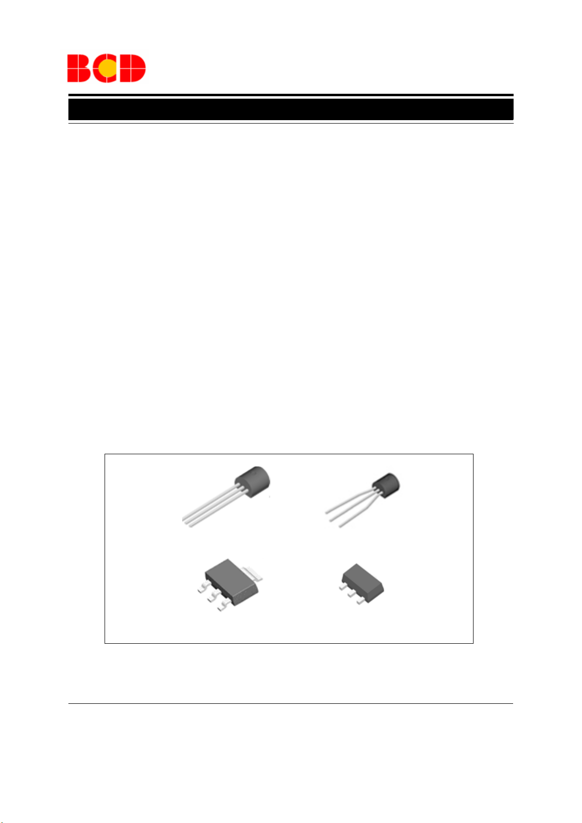
The AZ78LXX are available in the plastic TO-92
(bulk or ammo packing), SOT-223 and SOT-89 packages.
Features
· Output Current up to 100mA
· Fixed Output Voltages of 5V, 8V, 9V and 12V
· Output Voltage Tolerances of ±5% over the Full
Temperature Range
· Internal Short Circuit Current-limiting
· Internal Thermal Overload Protection
· No External Components
Applications
· High Efficiency Linear Regulator
· Post Regulation for Switching Supply
· Microprocessor Power Supply
· Mother Board I/O Power Supply
TO-92(Bulk Packing)
SOT-223
Figure 1. Package Types of the AZ78LXX
Nov. 2012 Rev. 2. 2 BCD Semiconductor Manufacturing Limited
TO-92(Ammo Packing)
SOT-89
1
Page 2
Data Sheet
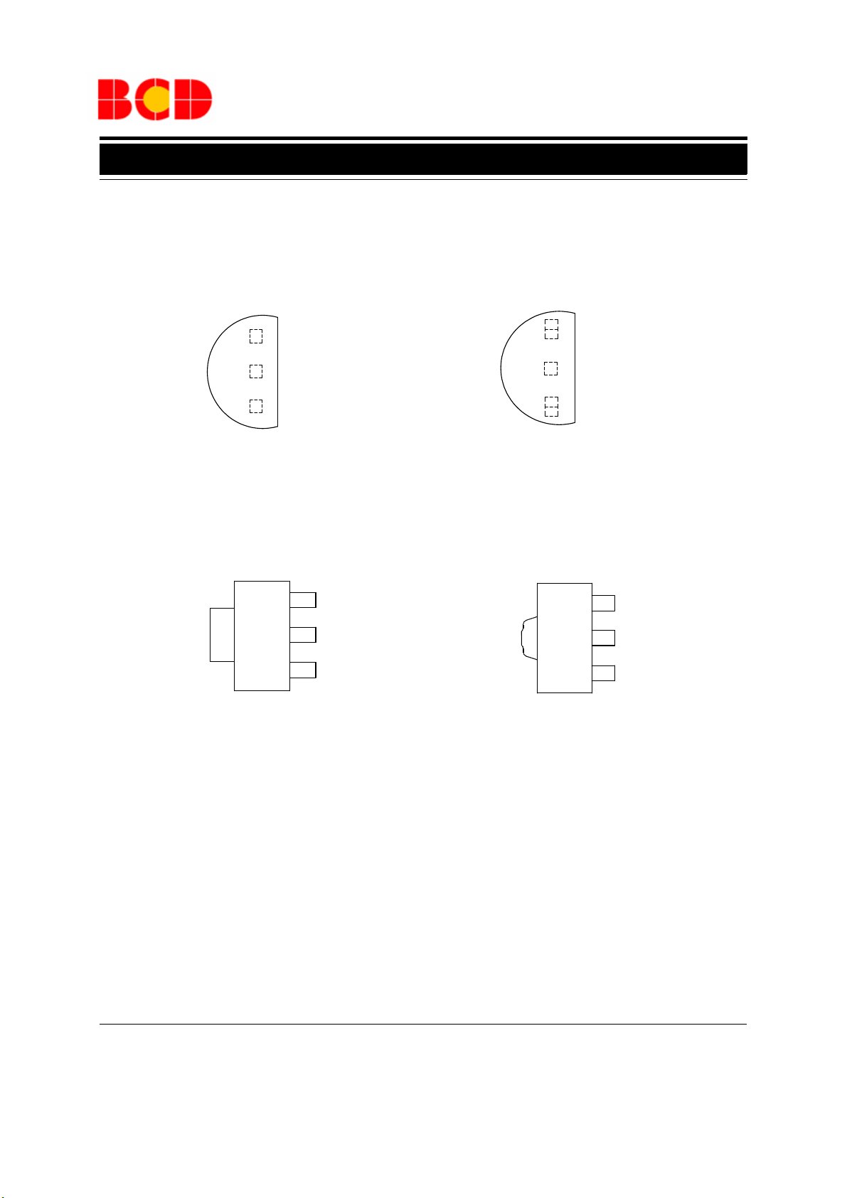
INPUT
OUTPUT
GND
1
2
3
4
GND
1
2
3
INPUT
OUTPUT
GND
GND
4
1
2
3
INPUT
OUTPUT
GND
1
2
3
INPUT
OUTPUT
GND
3-TERMINAL POSITIVE LINEAR REGULATOR AZ78LXX
Pin Configuration
Z Package
(TO-92(Bulk Packing))
H Package
(SOT-223)
Z Package
(TO-92(Ammo Packing))
R Package
(SOT-89)
Connect pin 4 to pin 2 or leave
electrically isolated pin 4
Figure 2. Pin Configuration of the AZ78LXX (Top View)
Nov. 2012 Rev. 2. 2 BCD Semiconductor Manufacturing Limited
2
Page 3
Data Sheet
3-TERMINAL POSITIVE LINEAR REGULATOR AZ78LXX
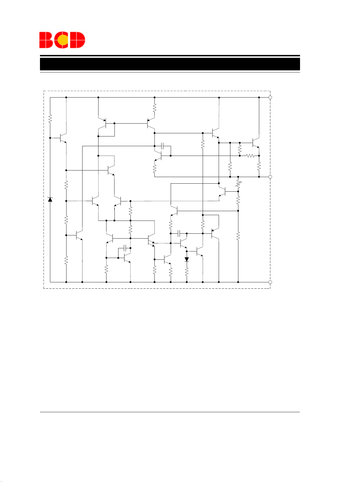
Functional Block Diagram
3 (8)
INPUT
1
OUTPUT
Figure 3. Functional Block Diagram of the AZ78LXX
2, 4 (2, 3, 6, 7)
A(B)
A for 3-pin
B for 8-pin
GND
Nov. 2012 Rev. 2. 2 BCD Semiconductor Manufacturing Limited
3
Page 4
Data Sheet
3-TERMINAL POSITIVE LINEAR REGULATOR AZ78LXX
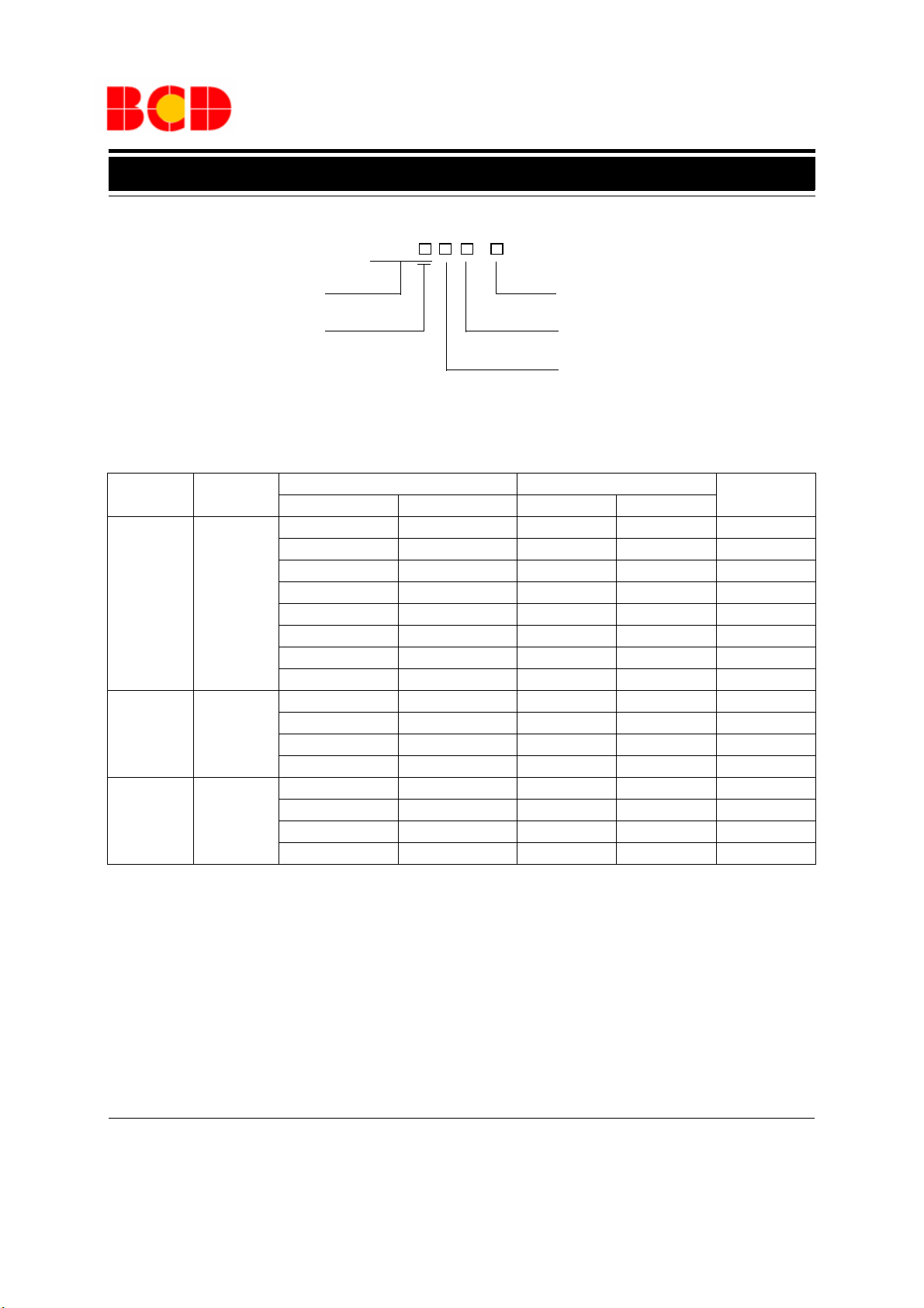
Ordering Information
Package
TO-92
SOT-89
SOT-223
Circuit Type
Output Voltage
05: 5V
08: 8V
09: 9V
12: 12V
Te mp er a tu re
Range
-40 to 125
-40 to 125
-40 to 125
o
C
o
C
o
C
AZ78L
-
E1: Lead Free
G1: Green
TR: Tape and Reel or Ammo
Blank: Tube or Bulk
Package
Z: TO-92
R: SOT-89
H: SOT-223
Part Number Marking ID
Lead Free Green Lead Free Green
AZ78L05Z-E1 AZ78L05Z-G1 AZ78L05Z-E1 AZ78L05Z-G1 Bulk
AZ78L05ZTR-E1 AZ78L05ZTR-G1 AZ78L05Z-E1 AZ78L05Z-G1 Ammo
AZ78L08Z-E1 AZ78L08Z-G1 AZ78L08Z-E1 AZ78L08Z-G1 Bulk
AZ78L08ZTR-E1 AZ78L08ZTR-G1 AZ78L08Z-E1 AZ78L08Z-G1 Ammo
AZ78L09Z-E1 AZ78L09Z-G1 AZ78L09Z-E1 AZ78L09Z-G1 Bulk
AZ78L09ZTR-E1 AZ78L09ZTR-G1 AZ78L09Z-E1 AZ78L09Z-G1 Ammo
AZ78L12Z-E1 AZ78L12Z-G1 AZ78L12Z-E1 AZ78L12Z-G1 Bulk
AZ78L12ZTR-E1 AZ78L12ZTR-G1 AZ78L12Z-E1 AZ78L12Z-G1 Ammo
AZ78L05RTR-E1 AZ78L05RTR-G1 E78A G78A Tape & Reel
AZ78L08RTR-E1 AZ78L08RTR-G1 E78B G78B Tape & Reel
AZ78L09RTR-E1 AZ78L09RTR-G1 E78C G78C Tape & Reel
AZ78L12RTR-E1 AZ78L12RTR-G1 E78D G78D Tape & Reel
AZ78L05HTR-E1 AZ78L05HTR-G1 EH78A GH78A Tape & Reel
AZ78L08HTR-E1 AZ78L08HTR-G1 EH78B GH78B Tape & Reel
AZ78L09HTR-E1 AZ78L09HTR-G1 EH78C GH78C Tape & Reel
AZ78L12HTR-E1 AZ78L12HTR-G1 EH78D GH78D Tape & Reel
Packing Type
BCD Semiconductor's Pb-free products, as designated with "E1" suffix in the part number, are RoHS compliant. Products with
"G1" suffix are available in green packages.
Nov. 2012 Rev. 2. 2 BCD Semiconductor Manufacturing Limited
4
Page 5
Data Sheet
3-TERMINAL POSITIVE LINEAR REGULATOR AZ78LXX
Absolute Maximum Ratings (Note 1)
Parameter Symbol Value Unit
Input Voltage V
Operating Junction Temperature T
Lead Temperature (Soldering, 10sec) T
Power Dissipation (T
Storage Temperature Range T
ESD (Human Body Model) ESD 2000 V
ESD (Machine Model) ESD 200 V
Note 1: Stresses greater than those listed under "Absolute Maximum Ratings" may cause permanent damage to
=25oC)
A
IN
J
LEAD
P
D
STG
TO-92 0.65
SOT-223 0.7
SOT-89 0.65
20 V
150
260
-65 to 150
o
o
W
o
C
C
C
the device. These are stress ratings only, and functional operation of the device at these or any other conditions
beyond those indicated under "Recommended Operating Conditions" is not implied. Exposure to "Absolute Maximum Ratings" for extended periods may affect device reliability.
Recommended Operating Conditions
Parameter Symbol Min Max Unit
Input Voltage
AZ78L05
AZ78L08 18
V
IN
15
V
AZ78L09 18
AZ78L12 18
Operating Junction Temperature T
-40 125
J
o
C
Nov. 2012 Rev. 2. 2 BCD Semiconductor Manufacturing Limited
5
Page 6
Data Sheet
3-TERMINAL POSITIVE LINEAR REGULATOR AZ78LXX
Electrical Characteristics
AZ78L05 Electrical Characteristics
ΔV
o
C, Bold typeface applies over -40oC to 125oC, I
4.8 5 5.2
OUT
RLINE
RLOAD
DROP
LIMIT
Q
Q
O
PK
/ ΔTI
OUT
7.0V ≤ V
1.0mA ≤ I
≤ 15V
IN
≤ 40mA (Note 2)
OUT
7.0V ≤ VIN≤ 15V
1.0mA ≤ I
OUT
≤ 100mA
TJ=25oC
I
=0 3 5 mA
OUT
8.0V ≤ VIN≤ 15V
1.0mA ≤ I
OUT
≤ 40mA
10Hz ≤ f ≤ 100kHz (Note 3)
f=120Hz, 8.0V ≤ V
= 5.0mA 0.65
OUT
IN
≤ 15V
4.75 5.25
=40mA, C
OUT
V
18 75 mV
20 60 mV
1.6 V
150 mA
1.0 mA
0.1
40 μV
47 62 dB
150 mA
mV/
Limits in standard typeface are for TJ=25
=0.33μF, C
Parameter Symbol Conditions Min Typ Max Unit
Output Voltage V
Line Regulation V
Load Regulation V
Dropout Voltage V
Current Limit I
Quiescent Current I
Quiescent Current Change ΔI
Output Noise Voltage N
Ripple Rejection PSRR
Peak Output Current I
Average Temperature Coefficient of
Output Voltage
=0.1μF, VIN=10V, unless otherwise specified.
OUT
IN
o
C
Minimum Value of Input Voltage
Required to Maintain Line Regula-
V
IN
6.7 7
V
(Min)
tion
TO-92 81
Thermal Resistance
θ
SOT-89 29.8
JC
o
C/W
SOT-223 71
Note 2: Power Dissipation ≤ 0.6W
Note 3: Recommended minimum load capacitance of 0.01μF to limit high frequency noise.
Nov. 2012 Rev. 2. 2 BCD Semiconductor Manufacturing Limited
6
Page 7

Data Sheet
3-TERMINAL POSITIVE LINEAR REGULATOR AZ78LXX
Electrical Characteristics (Continued)
AZ78L08 Electrical Characteristics
Limits in standard typeface are for TJ=25
=0.33μF, C
Parameter Symbol Conditions Min Typ Max Unit
Output Voltage V
Line Regulation V
Load Regulation V
Dropout Voltage V
Current Limit I
Quiescent Current I
Quiescent Current Change ΔI
Output Noise Voltage N
Ripple Rejection PSRR
Peak Output Current I
Average Temperature Coefficient of
Output Voltage
=0.1μF, VIN=14V, unless otherwise specified.
OUT
ΔV
o
C, Bold typeface applies over -40oC to 125oC, I
7.7 8.0 8.3
OUT
RLINE
RLOAD
DROP
LIMIT
Q
Q
O
PK
/ ΔTI
OUT
11V ≤ VIN≤ 18V
1.0mA ≤ I
≤ 40mA (Note
OUT
11V ≤ VIN≤ 18V
1.0mA ≤ I
OUT
≤ 100mA
TJ=25oC
I
=0 3 5 mA
OUT
11V ≤ VIN≤ 18V
1.0mA ≤ I
OUT
≤ 40mA
10Hz ≤ f ≤ 100kHz (Note 3)
f=120Hz, 11V ≤ V
= 5.0mA 0.8
OUT
IN
≤ 18V
7.6 8.4
39 45 dB
=40mA, C
OUT
V
18 75 mV
20 90 mV
1.6 V
150 mA
1.5 mA
0.1
60 μV
150 mA
mV/
o
IN
C
Minimum Value of Input Voltage
(Min) 9.7 V
V
IN
Required to Maintain Line Regulation
TO-92 81
Thermal Resistance
θ
SOT-89 84
JC
o
C/W
SOT-223 71
Note 2: Power Dissipation ≤ 0.6W
Note 3: Recommended minimum load capacitance of 0.01μF to limit high frequency noise.
Nov. 2012 Rev. 2. 2 BCD Semiconductor Manufacturing Limited
7
Page 8

Data Sheet
3-TERMINAL POSITIVE LINEAR REGULATOR AZ78LXX
Electrical Characteristics (Continued)
AZ78L09 Electrical Characteristics
ΔV
o
C, Bold typeface applies over -40oC to 125oC, I
8.6 9 9.4
OUT
RLINE
RLOAD
DROP
LIMIT
Q
Q
O
PK
/ ΔTI
OUT
12V ≤ V
1.0mA ≤ I
≤ 18V
IN
≤ 40mA (Note 2)
OUT
12V ≤ VIN≤ 18V
1.0mA ≤ I
OUT
≤ 100mA
TJ=25oC
I
=0 3 5 mA
OUT
12V ≤ VIN≤ 18V
1.0mA ≤ I
OUT
≤ 40mA
10Hz ≤ f ≤ 100kHz (Note 3)
f=120Hz, 12V ≤ V
= 5.0mA 0.9
OUT
IN
≤ 18V
8.55 9.45
38 44 dB
=40mA, C
OUT
V
18 75 mV
20 90 mV
1.6 V
150 mA
1.5 mA
0.1
70 μV
150 mA
mV/
Limits in standard typeface are for TJ=25
=0.33μF, C
Parameter Symbol Conditions Min Typ Max Unit
Output Voltage V
Line Regulation V
Load Regulation V
Dropout Voltage V
Current Limit I
Quiescent Current I
Quiescent Current Change ΔI
Output Noise Voltage N
Ripple Rejection PSRR
Peak Output Current I
Average Temperature Coefficient of
Output Voltage
=0.1μF, VIN =15V, unless otherwise specified.
OUT
IN
o
C
Minimum Value of Input Voltage
(Min) 10.7 V
V
IN
Required to Maintain Line Regulation
TO-92 81
Thermal Resistance
θ
JC
SOT-89 84
o
C/W
SOT-223 71
Note 2: Power Dissipation ≤ 0.6W
Note 3: Recommended minimum load capacitance of 0.01μF to limit high frequency noise.
Nov. 2012 Rev. 2. 2 BCD Semiconductor Manufacturing Limited
8
Page 9

Data Sheet
3-TERMINAL POSITIVE LINEAR REGULATOR AZ78LXX
Electrical Characteristics (Continued)
AZ78L12 Electrical Characteristics
ΔV
o
C, Bold typeface applies over -40oC to 125oC, I
11.5 12 12.5
OUT
RLINE
RLOAD
DROP
LIMIT
Q
Q
O
PK
/ ΔTI
OUT
15V ≤ V
1.0mA ≤ I
≤ 18V
IN
≤ 40mA (Note 2)
OUT
15V ≤ VIN≤ 18V
1.0mA ≤ I
OUT
≤ 100mA
TJ=25oC
I
=0 3 5 mA
OUT
15V ≤ VIN≤ 18V
1.0mA ≤ I
OUT
≤ 40mA
10Hz ≤ f ≤ 100kHz (Note 3)
f=120Hz, 15V ≤ V
= 5.0mA 1.0
OUT
IN
≤ 18V
11.4 12.6
40 54 dB
=40mA, C
OUT
V
18 75 mV
20 90 mV
1.6 V
150 mA
1.5 mA
0.1
80 μV
150 mA
mV/
Limits in standard typeface are for TJ=25
=0.33μF, C
Parameter Symbol Conditions Min Typ Max Unit
Output Voltage V
Line Regulation V
Load Regulation V
Dropout Voltage V
Current Limit I
Quiescent Current I
Quiescent Current Change ΔI
Output Noise Voltage N
Ripple Rejection PSRR
Peak Output Current I
Average Temperature Coefficient of
Output Voltage
=0.1μF, VIN=18V, unless otherwise specified.
OUT
IN
o
C
Minimum Value of Input Voltage
(Min) 13.7 V
V
IN
Required to Maintain Line Regulation
TO-92 81
Thermal Resistance
θ
SOT-89 84
JC
o
C/W
SOT-223 71
Note 2: Power Dissipation ≤ 0.6W
Note 3: Recommended minimum load capacitance of 0.01μF to limit high frequency noise.
Nov. 2012 Rev. 2. 2 BCD Semiconductor Manufacturing Limited
9
Page 10

Data Sheet
-40 -20 0 20 40 60 80 100 120
0.0
0.2
0.4
0.6
0.8
1.0
1.2
1.4
1.6
1.8
2.0
I
OUT
=1mA
I
OUT
=40mA
I
OUT
=100mA
Dropout Voltage (V)
Junction Temperature (oC)
AZ78L05
ΔV=1%*V
OUT
0246810
0
1
2
3
4
5
Output Voltage (V)
VI input voltage (V)
AZ78L05
V
OUT
=5V
T
J
=25
o
C
I
OUT
=100mA
I
OUT
=40mA
I
OUT
=1mA
Input Voltage (V)
-40 -20 0 20 40 60 80 100 120
2.2
2.3
2.4
2.5
2.6
2.7
2.8
2.9
3.0
Quiescent Current (mA)
Junction Temperature (oC)
AZ78L05
V
IN
=10V
I
OUT
=5mA
0 2 4 6 8 10 12 14 16 18 20
0.0
0.5
1.0
1.5
2.0
2.5
3.0
AZ78L05
V
OUT
=5.0V
I
OUT
=40mA
T
J
=25oC
Input Bias Current (mA)
Input Voltage (V)
3-TERMINAL POSITIVE LINEAR REGULATOR AZ78LXX
Typical Performance Characteristics
Figure 4. Dropout Characteristics
Nov. 2012 Rev. 2. 2 BCD Semiconductor Manufacturing Limited
Figure 5. Dropout Voltage vs. Junction Temperature
Figure 7. Input Bias Current vs. Input Voltage Figure 6. Quiescent Current vs. Junction Temperature
10
Page 11

Data Sheet
3-TERMINAL POSITIVE LINEAR REGULATOR AZ78LXX
Typical Performance Characteristics (Continued)
11. 5
11
10.5
(0.5V/Div)
IN
10
20
0
(20mV/D iv) V
-20
OUT
ΔV
-40
(Conditions: V
AZ78L05
Time (4μs/Div)
Figure 8. Line Transient Response
=10 to 11V, V
IN
OUT
=5V, I
OUT
=40mA)
75
50
25
(25mA/Div)
0
OUT
I
0
-100
(100mV/Div)
OUT
-200
ΔV
-300
Time (10μs/Div)
Figure 9. Load Transient Response
(Conditions: VIN=10V, V
OUT
=5V, I
AZ78L05
=1 to 50mA)
OUT
Nov. 2012 Rev. 2. 2 BCD Semiconductor Manufacturing Limited
11
Page 12

Data Sheet
AZ78L05
+
+
0.33μF
(Note 4)
0.1μF
(Note 4)
V
IN
V
OUT
1
2
3
3-TERMINAL POSITIVE LINEAR REGULATOR AZ78LXX
Typical Application
Note 4: Bypass capacitors are recommended for optimum stability and transient response and should be located
as close as possible to the regulator.
Figure 10. Typical Application of the AZ78LXX
Nov. 2012 Rev. 2. 2 BCD Semiconductor Manufacturing Limited
12
Page 13

Data Sheet
2.420(0.095)
2.660(0.105)
0.360(0.014)
0.760(0.030)
Φ
1.600(0.063)
MAX
12.500(0.492)
15.500(0.610)
1.270(0.050)
TYP
3.300(0.130)
3.700(0.146)
4.300(0.169)
4.700(0.185)
1.000(0.039)
1.400(0.055)
4.400(0.173)
4.800(0.189)
3.430(0.135)
MIN
0.320(0.013)
0.510(0.020)
0.000(0.000)
0.380(0.015)
3-TERMINAL POSITIVE LINEAR REGULATOR AZ78LXX
Mechanical Dimensions
TO-92(Bulk Packing) Unit: mm(inch)
Nov. 2012 Rev. 2. 2 BCD Semiconductor Manufacturing Limited
13
Page 14

Data Sheet
Φ
4.300(0.169)
4.700(0.185)
1
2.500(0.492)14.500(0.571)
2.540(0. 100
)
Ty
p
1.270(0.050
)
Typ
0. (0. 015)
0.
550
(0.022
)
4.400(0. 173
)
4.
800
(
0.
189
)
3.430(0. 135
)
MIN
0.320(0. 013
)
0
.510(0.020)
0.000(0.000
)
0. 380(0.015
)
MAX
1.100(0. 043
1.400(0. 055
)
3.300(0.130)
3.800(0.150)
Φ
1.600(0.063)
)
380
2.500(0. 098
)
4.000(0.157
)
13. 000(0. 512
)
15.000(0.591
)
3-TERMINAL POSITIVE LINEAR REGULATOR AZ78LXX
Mechanical Dimensions (Continued)
TO-92(Ammo Packing) Unit: mm(inch)
Nov. 2012 Rev. 2. 2 BCD Semiconductor Manufacturing Limited
14
Page 15

Data Sheet
3.300(0.130)
3.700(0.146)
6.700(0.264)
7.300(0.287)
2.900(0.114)
3.100(0.122)
0.610(0.024)
0.810(0.032)
2.300(0.091)
TYP
6.300(0.248)
6.700(0.264)
1.750(0.069)
TYP
4.500(0.177)
4.700(0.185)
0.020(0.001)
0.100(0.004)
1.520(0.060)
1.800(0.071)
1.500(0.059)
1.700(0.067)
0
.
2
5
0
(
0
.
0
1
0
)
0
.
3
5
0
(
0
.
0
1
4
)
0.250(0.010)
0°
10°
0.900(0.035)
MIN
3-TERMINAL POSITIVE LINEAR REGULATOR AZ78LXX
Mechanical Dimensions (Continued)
SOT-223 Unit: mm(inch)
Nov. 2012 Rev. 2. 2 BCD Semiconductor Manufacturing Limited
15
Page 16

Data Sheet
45
1.030(0.041)REF
1.550(0.061)REF
4.400(0.173)
4.600(0.181)
0.900(0.035)
1.100(0.043)
3.950(0.156)
4.250(0.167)
3.000(0.118)
TYP
0.480(0.019)
2.300(0.091)
2.600(0.102)
0.320(0.013)
0.520(0.020)
3
10
2.060(0.081)REF
1.400(0.055)
1.600(0.063)
0.350(0.014)
0.450(0.018)
R0.150(0.006)
3
10
1.500(0.059)
0.320(0.013)REF
1.620(0.064)REF
2.210(0.087)REF
0.320(0.013)
0.520(0.020)
1.800(0.071)
3-TERMINAL POSITIVE LINEAR REGULATOR AZ78LXX
Mechanical Dimensions (Continued)
SOT-89 Unit: mm(inch)
Nov. 2012 Rev. 2. 2 BCD Semiconductor Manufacturing Limited
16
Page 17

BCD Semiconductor Manufacturing Limited
IMPORTANT NOTICE
IMPORTANT NOTICE
BCD Semiconductor Manufacturing Limited reserves the right to make changes without further notice to any products or specifi-
BCD Semiconductor Manufacturing Limited reserves the right to make changes without further notice to any products or specifi-
cations herein. BCD Semiconductor Manufacturing Limited does not assume any responsibility for use of any its products for any
cations herein. BCD Semiconductor Manufacturing Limited does not assume any responsibility for use of any its products for any
particular purpose, nor does BCD Semiconductor Manufacturing Limited assume any liability arising out of the application or use
particular purpose, nor does BCD Semiconductor Manufacturing Limited assume any liability arising out of the application or use
of any its products or circuits. BCD Semiconductor Manufacturing Limited does not convey any license under its patent rights or
of any its products or circuits. BCD Semiconductor Manufacturing Limited does not convey any license under its patent rights or
other rights nor the rights of others.
other rights nor the rights of others.
http://www.bcdsemi.com
MAIN SITE
MAIN SITE
- Headquarters
BCD Semiconductor Manufacturing Limited
BCD Semiconductor Manufactur ing Limited
- Wafer Fab
No. 1600, Zi Xing Road, Shanghai ZiZhu Science-based Industrial Park, 200241, China
Shanghai SIM-BCD Semiconductor Manufacturing Limited
Tel: +86-21-24162266, Fax: +86-21-24162277
800, Yi Shan Road, Shanghai 200233, China
Tel: +86-21-6485 1491, Fax: +86-21-5450 0008
REGIONAL SALES OFFICE
Shenzhen Office
REGIONAL SALES OFFICE
Shanghai SIM-BCD Semiconductor Manufacturing Co., Ltd., Shenzhen Office
Shenzhen Office
Unit A Room 1203, Skyworth Bldg., Gaoxin Ave.1.S., Nanshan District, Shenzhen,
Shanghai SIM-BCD Semiconductor Manufacturing Co., Ltd. Shenzhen Office
China
Advanced Analog Circuits (Shanghai) Corporation Shenzhen Office
Tel: +86-755-8826 7951
Room E, 5F, Noble Center, No.1006, 3rd Fuzhong Road, Futian District, Shenzhen 518026, China
Fax: +86-755-8826 7865
Tel: +86-755-8826 7951
Fax: +86-755-8826 7865
- Wafer Fab
BCD Semiconductor Manufacturing Limited
Shanghai SIM-BCD Semiconductor Manufacturing Co., Ltd.
- IC Design Group
800 Yi Shan Road, Shanghai 200233, China
Advanced Analog Circuits (Shanghai) Corporation
Tel: +86-21-6485 1491, Fax: +86-21-5450 0008
8F, Zone B, 900, Yi Shan Road, Shanghai 200233, China
Tel: +86-21-6495 9539, Fax: +86-21-6485 9673
Taiwan Office
BCD Semiconductor (Taiwan) Company Limited
Taiwan Office
4F, 298-1, Rui Guang Road, Nei-Hu District, Taipei,
BCD Semiconductor (Taiwan) Company Limited
Tai wan
4F, 298-1, Rui Guang Road, Nei-Hu District, Taipei,
Tel: +886-2-2656 2808
Taiwan
Fax: +886-2-2656 2806
Tel: +886-2-2656 2808
Fax: +886-2-2656 2806
USA Office
BCD Semiconductor Corp.
USA Office
30920 Huntwood Ave. Hayward,
BCD Semiconductor Corporation
CA 94544, USA
30920 Huntwood Ave. Hayward,
Tel : +1-510-324-2988
CA 94544, U.S.A
Fax: +1-510-324-2788
Tel : +1-510-324-2988
Fax: +1-510-324-2788
 Loading...