

Page 1
Data Sheet
MULTIPLE RS-232 DRIVERS AND RECEIVERS AZ75232
General Description
The AZ75232 combines three drivers and five receivers, which conform to the EIA/TIA-232-F and ITU
v.28 standards. Each receiver converts EIA/TIA-232-F
inputs to 5-V TTL/CMOS levels and each driver converts TTL/CMOS input levels into EIA/TIA-232-F
levels.
The flow-through pinout facilitates simple non-crossover board layout. The AZ75232 provides a one-chip
solution for the common 9-pin serial RS-232 interface
between data terminal and data communications equipment.
The AZ75232 is available in SOIC-20, SSOP-20 and
TSSOP-20 packages.
Features
· Single Chip with Easy Interface between UART
and Serial-Port Connector
· Meet the Requirement of EIA/TIA-232-F and
ITU v.28 Standards
· Designed to Support Data Rates up to 120kbit/s
· 3 Drivers and 5 Receivers
· Flow-through Pinout
Applications
· Mother Board
· Peripheral Equipment
SSOP-20SOIC-20 TSSOP-20
Figure 1. Package Types of AZ75232
Oct. 2009 Rev. 1. 7 BCD Semiconductor Manufacturing Limited
1
Page 2
Data Sheet
MULTIPLE RS-232 DRIVERS AND RECEIVERS AZ75232
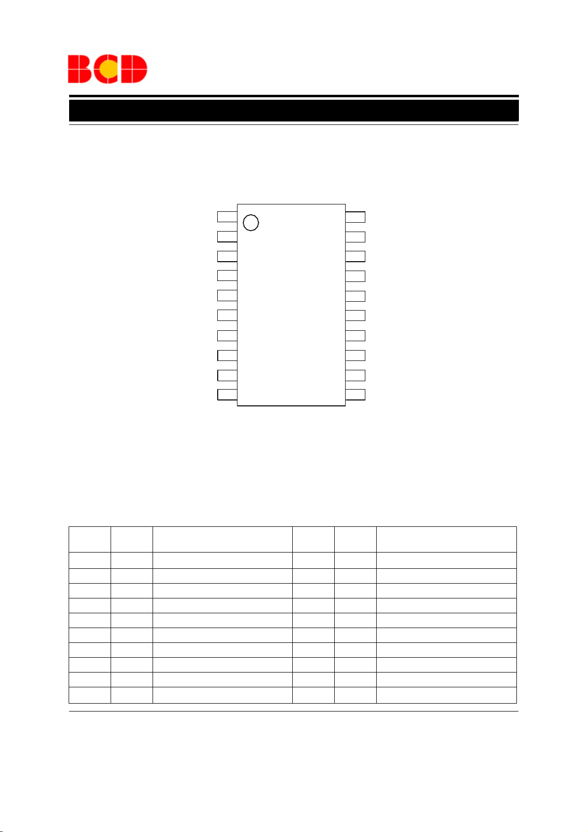
Pin Configuration
M/GS/G Package
(SOIC-20/SSOP-20/TSSOP-20)
V
RA1
RA2
RA3
DY1
DY2
RA4
DY3
RA5
V
DD
SS
1
2
3
4
5
6
7
8
9
10
20
19
18
17
16
15
14
13
12
11
V
CC
RY1
RY2
RY3
DA1
DA2
RY4
DA3
RY5
GND
Figure 2. Pin Configuration of AZ75232 (Top View)
Pin Description
Pin
Number
1
2 RA1 Receiver Input 12 RY5 Receiver Output
3 RA2 Receiver Input 13 DA3 Driver Input
4 RA3 Receiver Input 14 RY4 Receiver Output
5 DY1 Driver Output 15 DA2 Driver Input
6 DY2 Driver Output 16 DA1 Driver Input
7 RA4 Receiver Input 17 RY3 Receiver Output
8 DY3 Driver Output 18 RY2 Receiver Output
9 RA5 Receiver Input 19 RY1 Receiver Output
10
Oct. 2009 Rev. 1. 7 BCD Semiconductor Manufacturing Limited
Pin
Name
V
DD
V
SS
Function
Pin
Number
Pin
Name
Positive Supply Voltage for Driver 11 GND Ground
Negative Supply Voltage for Driver 20
V
Supply Voltage for Receiver
CC
2
Function
Page 3
Data Sheet
MULTIPLE RS-232 DRIVERS AND RECEIVERS AZ75232
Functional Block Diagram
V
RA1
RA2
RA3
DY1
DY2
RA4
DY3
RA5
V
1
DD
2
3
4
5
6
7
8
9
10
SS
20
19
18
17
16
15
14
13
12
11
Figure 3. Functional Block Diagram of AZ75232
V
CC
RY1
RY2
RY3
DA1
DA2
RY4
DA3
RY5
GND
Ordering Information
AZ75232 -
Circuit Type
Package
M: SOIC-20
GS: SSOP-20
G: TSSOP-20
Package
SOIC-20
SSOP-20
TSSOP-20
Te mp er a tu re
Range
o
-40 to 85
-40 to 85
-40 to 85
C
o
C
o
C
Lead Free Green Lead Free Green
AZ75232M-E1 AZ75232M-G1 AZ75232M-E1 AZ75232M-G1 Tube
AZ75232MTR-E1 AZ75232MTR-G1 AZ75232M-E1 AZ75232M-G1 Tape & Reel
AZ75232GS-E1 AZ75232GS-G1 AZ75232GS-E1 AZ75232GS-G1 Tube
AZ75232GSTR-E1 AZ75232GSTR-G1 AZ75232GS-E1 AZ75232GS-G1 Tape & Reel
AZ75232G-E1 AZ75232G-G1 232GE 232GG Tube
AZ75232GTR-E1 AZ75232GTR-G1 232GE 232GG Tape & Reel
BCD Semiconductor's Pb-free products, as designated with "E1" suffix in the part number, are RoHS compliant. Products with
"G1" suffix are available in green packages.
Part Number Marking ID
Oct. 2009 Rev. 1. 7 BCD Semiconductor Manufacturing Limited
E1: Lead Free
G1: Green
TR: Tape and Reel
Blank: Tube
Packing
Typ e
3
Page 4
Data Sheet
MULTIPLE RS-232 DRIVERS AND RECEIVERS AZ75232
Absolute Maximum Ratings (Note 1)
Parameter Symbol Value Unit
Supply Voltage
Input Voltage Range
Power Dissipation (T
=25oC)
A
Driver Output Voltage Range
Receiver Low-Level Output Current
Operating Junction Temperature
Storage Temperature Range
Lead Temperature (Soldering, 10sec)
V
V
V
T
T
LEAD
DD
CC
V
P
V
I
OL
T
STG
SS
D
I
Receiver -30 to 30
SOIC-20 1340
TSSOP-20 1100
O
J
Driver -15 to 7
15
-15
7
-15 to 15 V
20 mA
150
-65 to 150
260
V
V
mWSSOP-20 1210
o
C
o
C
o
C
Note 1: Stresses greater than those listed under "Absolute Maximum Ratings" may cause permanent damage to the device.
These are stress ratings only, and functional operation of the device at these or any other conditions beyond those indicated
under "Recommended Operating Conditions" is not implied. Exposure to "Absolute Maximum Ratings" for extended periods
may affect device reliability.
Recommended Operating Conditions
Parameter Symbol Min Max Unit
Supply Voltage
High-Level Input Voltage (Driver Only)
Low-Level Input Voltage (Driver Only)
High-Level Output Current
Low-Level Output Current
Operating Temperature Range
V
DD
V
SS
V
CC
V
IH
V
IL
Driver
Receiver -0.5
Driver
Receiver 16
I
OH
I
OL
T
A
7.5 15
-15 -7.5
4.5 5.5
1.9
0.8 V
-6
6
-40 85
V
V
mA
mA
o
C
Oct. 2009 Rev. 1. 7 BCD Semiconductor Manufacturing Limited
4
Page 5

Data Sheet
MULTIPLE RS-232 DRIVERS AND RECEIVERS AZ75232
Electrical Characteristics
(TA=25oC, unless otherwise specified.)
Parameter Symbol Conditions Min Typ Max Unit
VOLTAGE SUPPLY SECTION (V
Supply Current from V
Supply Current from V
Supply Current from V
DRIVER SECTION (V
DD
SS
CC
=5V, VDD=9V, VSS=-9V, unless otherwise specified)
CC
High-Level Output Voltage
Low-Level Output Voltage
High-Level Input Current
Low-Level Input Current
High-Level Short-Circuit
Output Current
Low-Level Short-Circuit Output Current
Output Resistance
DRIVER SECTION (V
=5V, VDD=12V, VSS=-12V, unless otherwise specified)
CC
Propagation Delay Time
Low to High Level Output
Propagation Delay Time
High to Low Level Output
Transition Time
Low to High Level Output
Transition Time
High to Low Level Output
=5V, VDD=9V, VSS=-9V, unless otherwise specified)
CC
V
=9V, VSS=-9V
DD
V
=12V, VSS=-12V
DD
=15V, VSS=-15V
V
DD
=9V, VSS=-9V
V
DD
=12V, VSS=-12V
V
DD
=15V, VSS=-15V
V
DD
=9V, VSS=-9V
V
DD
V
=12V, VSS=-12V
DD
V
=15V, VSS=-15V
DD
=9V, VSS=-9V
V
DD
=12V, VSS=-12V
V
DD
=15V, VSS=-15V
V
DD
I
DD
I
SS
I
CC
V
V
I
IH
I
I
OS(H)
I
OS(L)
r
t
PLH
t
PHL
All inputs at
1.9V, no load
All inputs at
0.8V, no load
All inputs at
1.9V, no load
All inputs at
0.8V, no load
All inputs at 5V, no load, VCC=5V
VIL=0.8V, RL=3kΩ
OH
VIH=1.9V, RL=3kΩ
OL
VI=5V
VI=0V
IL
VIL=0.8V, VO=0V
VIH=2V, VO=0V
VCC=VDD=VSS=0, VO=-2Vto 2V
O
RL=3kΩ to 7kΩ, CL=15pF
RL=3kΩ to 7kΩ, CL=15pF
CL=15pF
t
TLH
t
THL
RL=3kΩ to 7kΩ
RL=3kΩ to 7kΩ
=2500pF (Note 2)
C
L
C
=15pF
L
C
=2500pF (Note 2)
L
15
19
25
4.5
mA
5.5
9
-15
-19
-25
-3.2
mA
-3.2
-3.2
30
mA
67.5 V
-7.5 -6 V
10 µA
-1.6 mA
-4.5 -12 -19.5 mA
4.5 12 19.5 mA
300 Ω
315 500 ns
75 175 ns
60 100 ns
1.7 2.5 µs
40 75 ns
1.5 2.5 µs
Oct. 2009 Rev. 1. 7 BCD Semiconductor Manufacturing Limited
5
Page 6

Data Sheet
MULTIPLE RS-232 DRIVERS AND RECEIVERS AZ75232
Electrical Characteristics (Continued)
(T
=25oC, unless otherwise specified.)
A
Parameter Symbol Conditions Min Typ Max Unit
RECEIVER SECTION (V
Positive-Going Input Threshold Voltage
Negative-Going Input
Threshold Voltage
Input Hysteresis Voltage
High-Level Output Voltage
Low-Level Output Voltage
High-Level Input Current
Low-Level Input Current
Short-Circuit Output Current
RECEIVER SECTION (V
Propagation Delay Time
Low to High Level Output
Propagation Delay Time
High to Low Level Output
Transition Time
Low to High Level Output
Transition Time
High to Low Level Output
=5V, VDD=9V, VSS=-9V, unless otherwise specified)
CC
V
IT+
T
= -40 to 85 oC
A
V
IT-
V
HYS
=0.75V
V
V
OHIOH
V
OLIOL
=-0.5mA
=10mA, VI=3V
IH
Input Open 2.6
VI=25V
I
IH
=3V
V
I
VI=-25V
I
IL
I
OS
=5V, VDD=12V, VSS=-12V, unless otherwise specified)
CC
=-3V
V
I
VI=0.8V
RL=5kΩ, CL=50pF
t
PLH
=1.5kΩ, CL=15pF
R
L
RL=5kΩ, CL=50pF
t
PHL
=1.5kΩ, CL=15pF
R
L
RL=5kΩ, CL=50pF
t
TLH
=1.5kΩ, CL=15pF
R
L
RL=5kΩ, CL=50pF
t
THL
=1.5kΩ, CL=15pF
R
L
1.75 1.9 2.3 V
1.55 2.3 V
0.75 0.97 1.25 V
0.5 V
2.6 4 5
0.2 0.45 V
3.6 8.3
0.43
-3.6 -8.3
-0.43
-3.4 -12 mA
105 250
100 160
60 150
42 100
170 350
90 175
16 60
15 50
V
mA
mA
ns
ns
ns
ns
Note 2: Measured between -3V and 3V points of the output waveform (EIA/TIA-232-F conditions); all unused
inputs are tied either high or low.
Oct. 2009 Rev. 1. 7 BCD Semiconductor Manufacturing Limited
6
Page 7

Data Sheet
MULTIPLE RS-232 DRIVERS AND RECEIVERS AZ75232
Typical Performance Characteristics
12
9
6
3
0
-3
-6
Output Voltage (V)
-9
-12
0.0 0.2 0.4 0.6 0.8 1.0 1.2 1.4 1.6 1.8 2.0
VDD=12V, VSS=-12V
VDD=9V, VSS=-9V
VDD=6V, VSS=-6V
RL=3K
T
=25oC
A
Input Voltage (V)
Figure 4. Voltage Transfer Characteristics
Driver Section
20
16
12
-4
Output Current (mA)
-8
-12
-16
-20
VDD=9V
=-9V
V
SS
T
=25oC
A
8
4
0
VOL(VI=1.9V)
VOH(VI=0.8V)
-16 -12 -8 -4 0 4 8 12 16
Output Voltage (V)
Figure 5. Output Current vs. Output Voltage
18
15
12
I
9
6
VDD=9V
3
=-9V
V
SS
=0
V
O
0
-3
-6
Short-Circuit Output Current (mA)
-9
-12
-40 -20 0 20 40 60 80
OS(L)(VI
I
OS(H)(VI
=1.9V)
=0.8V)
Temperature (oC)
Figure 6. Short-Circuit Output Current vs. Temperature
1000
VDD = 9V
V
= -9V
SS
= 3K
R
100
10
Slew Rate (V/µs)
L
T
A
= 25oC
Slew Rate of Fall Edge
Slew Rate of Rise Edge
1
10 100 1000 10000
Load Capacitance (pF)
Figure 7. Slew Rate vs. Load Capacitance
Oct. 2009 Rev. 1. 7 BCD Semiconductor Manufacturing Limited
7
Page 8

Data Sheet
MULTIPLE RS-232 DRIVERS AND RECEIVERS AZ75232
Typical Performance Characteristics (Continued)
Receiver Section
2.4
2.2
2.0
1.8
1.6
1.4
1.2
1.0
Input Thresho ld Voltage (V)
0.8
0.6
0.4
-40 -20 0 20 40 60 80
V
IT+
V
IT-
Temperature (oC)
Figure 8. Input Threshold Voltage vs. Temperature
6
5
VCC = 5V
T
= 25oC
A
2.0
1.8
1.6
1.4
1.2
1.0
0.8
0.6
Input Threshold Voltage (V)
0.4
0.2
0.0
2345678
V
IT+
V
IT-
Supply Voltage (V)
Figure 9. Input Threshold Voltage vs. Supply Voltage
4
3
Amplitude (V)
2
1
0
10 100 1000 10000
CL=12pF
CL=500pF
Pulse Duratio n (ns)
Figure 10. Noise Rejection
Oct. 2009 Rev. 1. 7 BCD Semiconductor Manufacturing Limited
8
Page 9

Data Sheet
MULTIPLE RS-232 DRIVERS AND RECEIVERS AZ75232
Typical Application
EIA/TIA-232-F
DB9S
TTL/CMOS
Level
UART
or
Serial µC
RI
DTR
CTS
TX
RTS
RX
DSR
DCD
5V
12
13
15
16
11
GND
RY5
DA3
14
RY4
AZ75232
DA2
DA1
17
RY3
18
RY2
19
RY1
20
V
CC
V
RA5
DY3
RA4
DY2
DY1
RA3
RA2
RA1
V
10
SS
DD
-12V
9
C3
C1
DTR
CTS
DSR
8
7
6
5
4
3
2
1
C2
12V
Signal
Ground
RI
TX
RTS
RX
DCD
CONNECTOR
5
9
6
1
Figure 11. Typical Application of AZ75232
Oct. 2009 Rev. 1. 7 BCD Semiconductor Manufacturing Limited
9
Page 10

Data Sheet
MULTIPLE RS-232 DRIVERS AND RECEIVERS AZ75232
Mechanical Dimensions
Unit: mm(inch)SOIC-20
Note: Eject hole, oriented hole and mold mark is optional.
Oct. 2009 Rev. 1. 7 BCD Semiconductor Manufacturing Limited
10
Page 11

Data Sheet
MULTIPLE RS-232 DRIVERS AND RECEIVERS AZ75232
Mechanical Dimensions (Continued)
Unit: mm(inch)SSOP-20
DETAIL
7.600(0.299)
8.000(0.315)
0.070(0.003)
0.230(0.009)
1.400(0.055)
1.600(0.063)
1.200(0.047)
DEP
1.200(0.047)
7.000(0.276)
7.400(0.291)
0.650(0.026)
ٛ 1.200(0.047)
φ
0.020(0.001)
0.080(0.003)
0.220(0.009)
0.380(0.015)
5.100(0.201)
5.500(0.217)
1
7
1.690(0.067)
MAX
0.250(0.010)
SEE DETAIL A
0.090(0.004)
0
0
0.250(0.010)
0
10
0
14
R0.150(0.006)
0.324(0.013)
R0.150(0.006)
0
1
0
7
0.630(0.025)
0.950(0.037)
1.250(0.049)
DETAIL A
1.700(0.067)
1.900(0.075)
OPTIONAL
CONSTRUCTION
Note: Eject hole, oriented hole and mold mark is optional
Oct. 2009 Rev. 1. 7 BCD Semiconductor Manufacturing Limited
11
Page 12

Data Sheet
MULTIPLE RS-232 DRIVERS AND RECEIVERS AZ75232
Mechanical Dimensions
Unit: mm(inch)TSSOP-20
6.400(0.252)
6.600(0.260)
Ф
INDEX
1.450(0.057)
Ф
1.550(0.061)
BTM E-MARK
0.750(0.030)
Ф
0.850(0.033)
0.000(0.000)
Dp
0.100(0.004)
0.000(0.000)
Dp
0.100(0.004)
6.200(0.244)
6.600(0.260)
4.300(0.169)
4.500(0.177)
Ф
#1 PIN
0.650(0.026)TYP
0.200(0.008)
0.280(0.011)
0.800(0.031)
1.050(0.041)
0.340(0.013)
0.540(0.021)
1.200(0.047)
MAX
0.050(0.002)
0.150(0.006)
0.200(0.008)MIN
R0.090(0.004)MIN
R0.090(0.004)MIN
0.250(0.010)TYP
0.100(0.004)
0.190(0.007)
4-
TOP & BOTTOM
10°
14°
0°
8°
0.450(0.018)
0.750(0.030)
Note: Eject hole, oriented hole and mold mark is optional.
1.000(0.039)
REF
Oct. 2009 Rev. 1. 7 BCD Semiconductor Manufacturing Limited
12
Page 13

BCD Semiconductor Manufacturing Limited
IMPORTANT NOTICE
IMPORTANT NOTICE
BCD Semiconductor Manufacturing Limited reserves the right to make changes without further notice to any products or specifi-
BCD Semiconductor Manufacturing Limited reserves the right to make changes without further notice to any products or specifi-
cations herein. BCD Semiconductor Manufacturing Limited does not assume any responsibility for use of any its products for any
cations herein. BCD Semiconductor Manufacturing Limited does not assume any responsibility for use of any its products for any
particular purpose, nor does BCD Semiconductor Manufacturing Limited assume any liability arising out of the application or use
particular purpose, nor does BCD Semiconductor Manufacturing Limited assume any liability arising out of the application or use
of any its products or circuits. BCD Semiconductor Manufacturing Limited does not convey any license under its patent rights or
of any its products or circuits. BCD Semiconductor Manufacturing Limited does not convey any license under its patent rights or
other rights nor the rights of others.
other rights nor the rights of others.
http://www.bcdsemi.com
MAIN SITE
MAIN SITE
- Headquarters
BCD Semiconductor Manufacturing Limited
BCD Semiconductor Manufactur ing Limited
- Wafer Fab
No. 1600, Zi Xing Road, Shanghai ZiZhu Science-based Industrial Park, 200241, China
Shanghai SIM-BCD Semiconductor Manufacturing Limited
Tel: +86-21-24162266, Fax: +86-21-24162277
800, Yi Shan Road, Shanghai 200233, China
Tel: +86-21-6485 1491, Fax: +86-21-5450 0008
REGIONAL SALES OFFICE
Shenzhen Office
REGIONAL SALES OFFICE
Shanghai SIM-BCD Semiconductor Manufacturing Co., Ltd., Shenzhen Office
Shenzhen Office
Unit A Room 1203, Skyworth Bldg., Gaoxin Ave.1.S., Nanshan District, Shenzhen,
Shanghai SIM-BCD Semiconductor Manufacturing Co., Ltd. Shenzhen Office
China
Advanced Analog Circuits (Shanghai) Corporation Shenzhen Office
Tel: +86-755-8826 7951
Room E, 5F, Noble Center, No.1006, 3rd Fuzhong Road, Futian District, Shenzhen 518026, China
Fax: +86-755-8826 7865
Tel: +86-755-8826 7951
Fax: +86-755-8826 7865
- Wafer Fab
BCD Semiconductor Manufacturing Limited
Shanghai SIM-BCD Semiconductor Manufacturing Co., Ltd.
- IC Design Group
800 Yi Shan Road, Shanghai 200233, China
Advanced Analog Circuits (Shanghai) Corporation
Tel: +86-21-6485 1491, Fax: +86-21-5450 0008
8F, Zone B, 900, Yi Shan Road, Shanghai 200233, China
Tel: +86-21-6495 9539, Fax: +86-21-6485 9673
Taiwan Office
BCD Semiconductor (Taiwan) Company Limited
Taiwan Office
4F, 298-1, Rui Guang Road, Nei-Hu District, Taipei,
BCD Semiconductor (Taiwan) Company Limited
Tai wan
4F, 298-1, Rui Guang Road, Nei-Hu District, Taipei,
Tel: +886-2-2656 2808
Taiwan
Fax: +886-2-2656 2806
Tel: +886-2-2656 2808
Fax: +886-2-2656 2806
USA Office
BCD Semiconductor Corp.
USA Office
30920 Huntwood Ave. Hayward,
BCD Semiconductor Corporation
CA 94544, USA
30920 Huntwood Ave. Hayward,
Tel : +1-510-324-2988
CA 94544, U.S.A
Fax: +1-510-324-2788
Tel : +1-510-324-2988
Fax: +1-510-324-2788
 Loading...