

Page 1
Data Sheet
VOLTAGE DETECTOR AZ70XX
General Description
The AZ70XX series ICs are under voltage detectors
with a built in voltage threshold and low power consumption. The AZ70XX are specifically designed to
accurately monitor power supplies.
The AZ70XX use a precision on-chip voltage reference and a comparator to measure the input operating
voltage. These ICs can accurately reset the system after
detecting voltage at the time of switching power on and
instantaneous power off in various CPU systems and
other logic systems. The detect voltage thresholds are
2.3V/2.5V/2.7V/2.9V/3.1V/3.3V/4.2V/4.5Vfor
AZ7023/25/27/29/31/33/42/45 respectively. Built in
hysteresis helps to prevent erratic operation in the presence of noise.
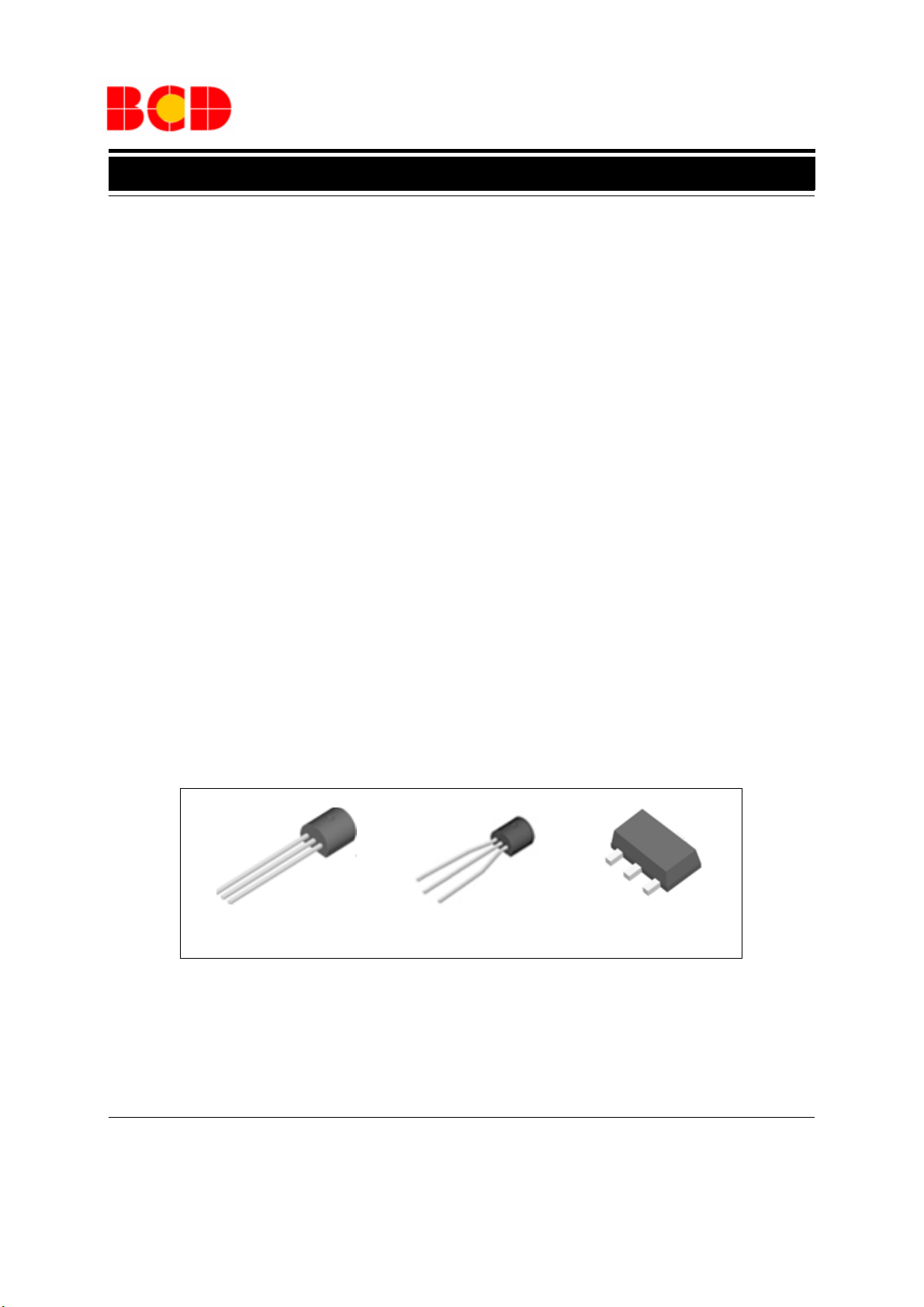
The AZ70XX series are available in 2 standard packages: TO-92 (bulk or ammo packing) and SOT-89.
Features
· Low Current Consumption:
I
=300µA Typical
CCL
I
=30µA Typical
CCH
· Low Minimum Operating Voltage for Output
Resetting: 0.8V Typical
· Built in Hysteresis Voltage: 50mV Typical
· Open Collector Output
o
· Extended Temperature Range: -40 to 85
C
Applications
· Low Battery Voltage Detector
· Power Fail Indicator
· Processor Reset Generator
· Battery Backup Control
· Home Electric Appliances
TO-92(Bulk Packing) TO-92(Ammo Packing)
Figure 1. Package Types of AZ70XX
SOT-89
Oct. 2011 Rev. 2. 2 BCD Semiconductor Manufacturing Limited
1
Page 2
Data Sheet
VOLTAGE DETECTOR AZ70XX
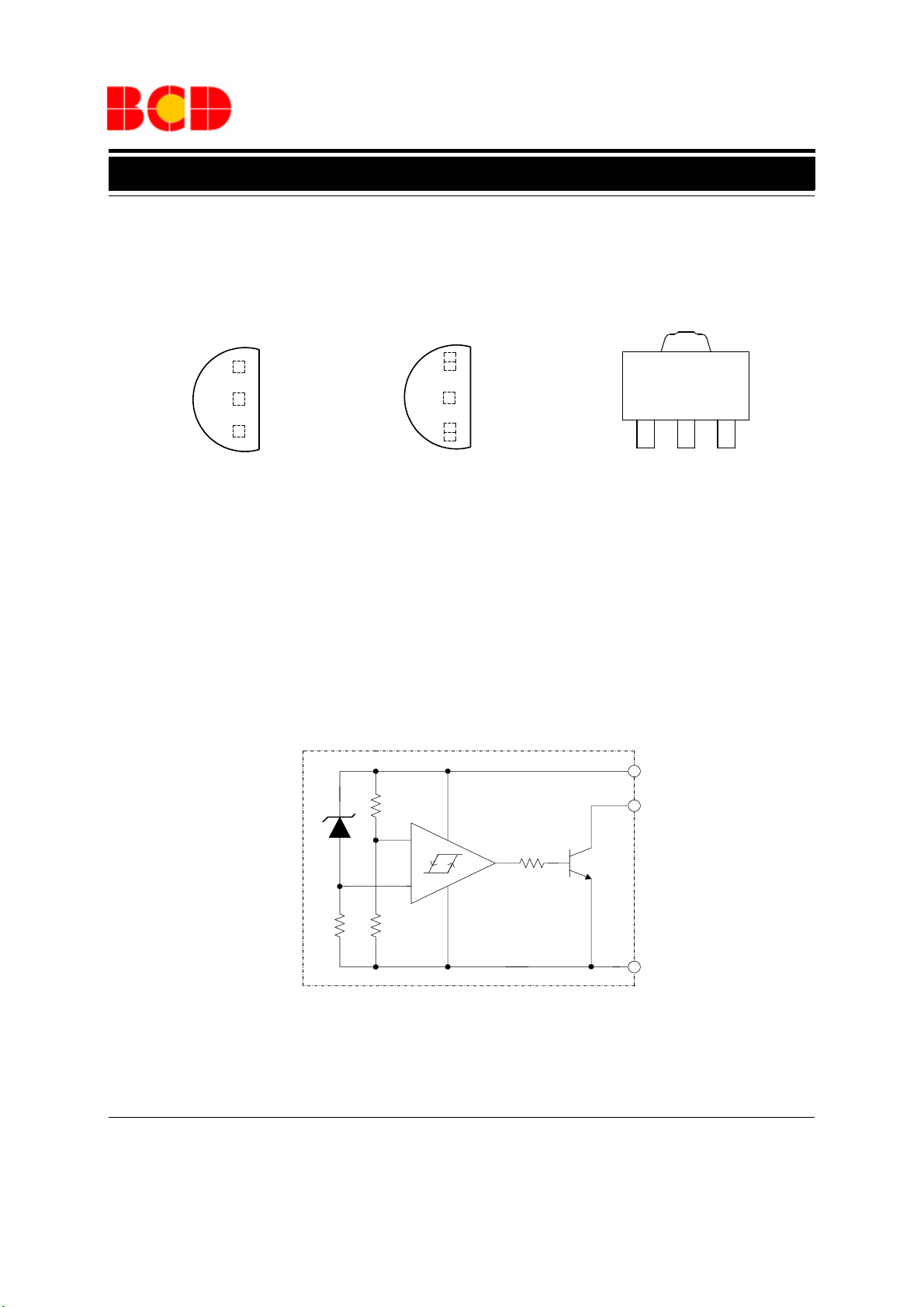
Pin Configuration
Z Package R Package
(TO-92(Bulk Packing)) (TO-92(Ammo Packing))
3
OUT
2
GND
1
V
CC
Figure 2. Pin Configuration of AZ70XX (Top View)
Functional Block Diagram
Z Package
3
OUT
2
GND
V
1
CC
(SOT-89)
123
V
GND OUT
CC
V
CC
OUT
+
-
GND
Figure 3. Functional Block Diagram of AZ70XX
Oct. 2011 Rev. 2. 2 BCD Semiconductor Manufacturing Limited
2
Page 3
Data Sheet
VOLTAGE DETECTOR AZ70XX
Ordering Information
AZ70
Circuit Type
-
E1: Lead Free
G1: Green
Package
TO-92
SOT-89
Detect Voltage
23: 2.3V
25: 2.5V
27: 2.7V
29: 2.9V
Temperature
Range
o
-40 to 85
-40 to 85
C
o
C
TR: Tape and Reel or Ammo
31: 3.1V
33: 3.3V
42: 4.2V
45: 4.5V
Detect
Voltage
2.3V
2.5V
2.7V
2.9V
3.1V
3.3V
4.2V
4.5V
2.3V AZ7023RTR-E1 AZ7023RTR-G1 E723 G70A Tape & Reel
2.5V AZ7025RTR-E1 AZ7025RTR-G1 E725 G70G Tape & Reel
2.7V AZ7027RTR-E1 AZ7027RTR-G1 E727 G70B Tape & Reel
2.9V AZ7029RTR-E1 AZ7029RTR-G1 E729 G70C Tape & Reel
3.1V AZ7031RTR-E1 AZ7031RTR-G1 E731 G70H Tape & Reel
3.3V AZ7033RTR-E1 AZ7033RTR-G1 E733 G70D Tape & Reel
4.2V AZ7042RTR-E1 AZ7042RTR-G1 E742 G70E Tape & Reel
4.5V AZ7045RTR-E1 AZ7045RTR-G1 E745 G70F Tape & Reel
AZ7023Z-E1 AZ7023Z-G1 AZ7023Z-E1 AZ7023Z-G1 Bulk
AZ7023ZTR-E1 AZ7023ZTR-G1 AZ7023Z-E1 AZ7023Z-G1 Ammo
AZ7025Z-E1 AZ7025Z-G1 AZ7025Z-E1 AZ7025Z-G1 Bulk
AZ7025ZTR-E1 AZ7025ZTR-G1 AZ7025Z-E1 AZ7025Z-G1 Ammo
AZ7027Z-E1 AZ7027Z-G1 AZ7027Z-E1 AZ7027Z-G1 Bulk
AZ7027ZTR-E1 AZ7027ZTR-G1 AZ7027Z-E1 AZ7027Z-G1 Ammo
AZ7029Z-E1 AZ7029Z-G1 AZ7029Z-E1 AZ7029Z-G1 Bulk
AZ7029ZTR-E1 AZ7029ZTR-G1 AZ7029Z-E1 AZ7029Z-G1 Ammo
AZ7031Z-E1 AZ7031Z-G1 AZ7031Z-E1 AZ7031Z-G1 Bulk
AZ7031ZTR-E1 AZ7031ZTR-G1 AZ7031Z-E1 AZ7031Z-G1 Ammo
AZ7033Z-E1 AZ7033Z-G1 AZ7033Z-E1 AZ7033Z-G1 Bulk
AZ7033ZTR-E1 AZ7033ZTR-G1 AZ7033Z-E1 AZ7033Z-G1 Ammo
AZ7042Z-E1 AZ7042Z-G1 AZ7042Z-E1 AZ7042Z-G1 Bulk
AZ7042ZTR-E1 AZ7042ZTR-G1 AZ7042Z-E1 AZ7042Z-G1 Ammo
AZ7045Z-E1 AZ7045Z-G1 AZ7045Z-E1 AZ7045Z-G1 Bulk
AZ7045ZTR-E1 AZ7045ZTR-G1 AZ7045Z-E1 AZ7045Z-G1 Ammo
Part Number Marking ID
Lead Free Green Lead Free Green
Blank: Bulk
Package
Z: TO-92
R: SOT-89
Packing
Typ e
BCD Semiconductor's Pb-free products, as designated with "E1" suffix in the part number, are RoHS compliant. Products with
"G1" suffix are available in green packages.
Oct. 2011 Rev. 2. 2 BCD Semiconductor Manufacturing Limited
3
Page 4
Data Sheet
VOLTAGE DETECTOR AZ70XX
Absolute Maximum Ratings (Note 1)
Parameter Symbol Value Unit
T
V
CC
P
T
STG
-0.3 to 20 V
TO-92 Package: 400
D
J
SOT-89 Package: 500
150
-65 to 150
mW
o
C
o
C
Supply Voltage
Power Dissipation (Package Limitations,
=25oC)
T
A
Operating Junction Temperature
Storage Temperature Range
Note 1: Stresses greater than those listed under "Absolute Maximum Ratings" may cause permanent damage to
the device. These are stress ratings only, and functional operation of the device at these or any other conditions
beyond those indicated under"Recommended Operating Conditions" is not implied. Exposure to "Absolute Maximum Ratings" for extended periods may affect device reliability.
Recommended Operating Conditions
Parameter Symbol Min Max Unit
Supply Voltage
Operating Temperature Range
V
CC
T
A
-40 85
18 V
o
C
Oct. 2011 Rev. 2. 2
BCD Semiconductor Manufacturing Limited
4
Page 5

Data Sheet
VOLTAGE DETECTOR AZ70XX
Electrical Characteristics
TA=25oC, unless otherwise specified.
Parameter Symbol Conditions Min Typ Max Unit
AZ7023R/Z 2.15 2.3 2.45
AZ7025R/Z 2.35 2.5 2.65
AZ7027R/Z 2.55 2.7 2.85
AZ7029R/Z 2.75 2.9 3.05
AZ7031R/Z 2.95 3.1 3.25
AZ7033R/Z 3.15 3.3 3.45
AZ7042R/Z 4.05 4.2 4.35
AZ7045R/Z 4.35 4.5 4.65
(min)-0.05V
30 50 100 mV
(min)-0.05V
(min)-
DET
=1.0KΩ,
L
(min)-0.05V
20
(min)-0.05V
16
0.4 V
0.1
±0.01
% /
300 500 µA
30 50
0.8 V
10 µs
15 µs
o
V
µA
µA
mA
C/W
Detect Vo l t a g e
Low-level Output Voltage
Output Leakage Current
Hysteresis Voltage
Detect Voltage Temperature
Coefficient
Circuit Current at On Time
Circuit Current at Off Time
Minimum Operating Voltage
“L” Transmission Delay Time
“H” Transmission Delay Time
Output Current at On Time
Thermal Resistance
(Junction to Case)
∆V
V
DET
V
OL
I
OH
V
HYS
/(V
DET
× ∆T)
I
CCL
I
CCH
V
OPR
tpHL
tpLH
Ⅰ
I
OL
Ⅱ
I
OL
θ
JC
RL=200Ω
(Note 2)
V
≤ 0.4V
OL
VCC=V
DET
=200Ω (Note 2)
R
L
VCC=18V
RL=200Ω (Note 2)
DET
R
=200Ω (Note 2)
L
VCC=V
DET
VCC=5.25V
RL=200Ω (Note 2)
V
≤ 0.4V
OL
V
changed from 5.25V to
CC
(min)-0.05V, RL=1.0KΩ,
V
DET
=100p (Note 3)
C
L
changed from V
V
CC
0.05V to 5.25V, R
=100p (Note 3)
C
L
V
CC=VDET
=25oC (Note 4)
T
A
V
CC=VDET
T
=-40 to 85 oC (Note 4)
A
TO-92 72
SOT-89 74
o
C
Note 2: See test circuit 1 and Figure 12.
Note 3: See test circuit 2 and Figure 12.
Note 4: See test circuit 3. Adjusting the regulative power source until the reading value of voltage meter V is 0.4V, the reading
value of current meter A is defined as "Output Current at On Time".
Oct. 2011 Rev. 2. 2
BCD Semiconductor Manufacturing Limited
5
Page 6

Data Sheet
VOLTAGE DETECTOR AZ70XX
Electrical Characteristics (Continued)
Input
Pulse
V1
A1
1
V
CC
AZ7029
OUT
GND
2
Figure 4. Test Circuit 1
1
V
CC
AZ7029
GND
2
OUT
3
A2
R
L
3
+
10µF
R
L
+
10µF
C
L
V2
+5V
Figure 5. Test Circuit 2
Figure 5. Test Circuit 2
1
V
V
(min)-0.05V
DET
+
10µF
AZ7029
GND
CC
2
OUT
3
A
V
Figure 6. Test Circuit 3
Oct. 2011 Rev. 2. 2 BCD Semiconductor Manufacturing Limited
6
Page 7

Data Sheet
VOLTAGE DETECTOR AZ70XX
Typical Performance Characteristics
2.95
AZ7029
2.90
V
(VCC Rising)
DET+
2.85
V
(VCC Falling)
Detect Voltage (V)
2.80
2.75
-40-20 0 20406080
DET-
Temperature (OC)
1200
1100
1000
900
800
700
600
500
Minimum Operating Voltage (mV)
400
-40-20 0 20406080
AZ7029
Temperature (OC)
Figure 7. Detect Voltage vs. Temperature Figure 8. Minimum Operating Voltage vs. Temperature
70
60
50
40
AZ7029
100
75
AZ7029
50
30
25
Output Current at On Time (mA)
20
10
-40-20 0 20406080
Temperature (OC)
Low-level Output Voltage (mV)
0
-40-20 0 20406080
Temperature (OC)
Figure 9. Output Current at On Time vs. Temperature Figure 10. Low-level Output Voltage vs. Temperature
Oct. 2011 Rev. 2. 2
BCD Semiconductor Manufacturing Limited
7
Page 8

Data Sheet
VOLTAGE DETECTOR AZ70XX
Typical Performance Characteristics (Continued)
Time (s)
Figure 11. Output Voltage Dynamic Response when V
Operating Diagram
V
CC
V
DET+
V
DET-
V
OPR
V
OUT
Increases and Decreases
CC
V
HYS
tpLHtpHL
tpHL tpLH
Figure 12. AZ70XX Timing Waveform (Note 5)
GND
Note 5: Detect voltage: V
DET-
Hysteresis voltage (V
HYS
): V
DET+-VDET-
Release voltage: V
DET+
Minimum operating voltage: V
OPR
Oct. 2011 Rev. 2. 2 BCD Semiconductor Manufacturing Limited
8
Page 9

Data Sheet
VOLTAGE DETECTOR AZ70XX
Operating Diagram (Continued)
Figure 12 is a typical timing waveform for AZ70XX.
In normal steady-state operation when V
output will be in a logic high state and V
the
CC>VDET-
OUT
dependent upon the voltage that the pull-up resistor
connected to.
Here is some explanations for AZ70XX's operation.
1. When the input voltage V
falls below V
CC
DET-
, the
output will pull down to logic low after a delay time of
tpHL. In general, at rated output current and V
V
can be pulled down to a voltage as low as within
OUT
CC
0.4V from GND. (See the Electrical Characteristics
section). The voltage level V
means the detect
DET-
voltage.
2. The output, V
, will stay valid until V
OUT
below the minimum operating voltage, V
OPR
falls
CC
(0.8V
Typical Applications
typical). Below minimum operating voltage, the output is undefined.
,
is
3. During power-up, V
rises above V
V
CC
become valid. V
while V
V
DET+
OPR
is the release voltage. V
<
VCC<
OPR
OUT
will remain undefined until
OUT
, at which time the output will
will be in its active low state
V
DET+ (VDET+=VDET-+VHYS
means the hystere-
HYS
sis voltage and is the difference voltage between the
,
and V
V
DET+
4. When V
.
DET-
rises above V
CC
, the output will be in
DET+
its inactive state. After a delay time of tpLH, V
will be in its logic high state .
).
OUT
1
V
CC
AZ70XX
GND
2
Figure 13. Low Voltage Indicator
Oct. 2011 Rev. 2. 2
OUT
V
GND
VCC +5V
CC
CPU
V
CC
OUT
R1
3.3k
3
C1
1 µF
RESET
+
R1
220
3
LED
AZ70XX
1
V
CC
GND
2
Figure 14. CPU Resetting Circuit
BCD Semiconductor Manufacturing Limited
9
Page 10

Data Sheet
VOLTAGE DETECTOR AZ70XX
Mechanical Dimensions
TO-92(Bulk Packing) Unit: mm(inch)
1.000(0.039)
1.400(0.055)
3.300(0.130)
3.700(0.146)
3.430(0.135)
MIN
4.400(0. 173)
4.800(0. 189)
Φ
1.600(0.063)
MAX
0.320(0.013)
0.510(0.020)
0.000(0.000)
0.380(0.015)
4.300(0.169)
4.700(0.185)
1.270(0.050)
TYP
0.360(0.014)
0.760(0.030)
12.500(0.492)
15.500(0.610)
2.420(0.095)
2.660(0.105)
Oct. 2011 Rev. 2. 2 BCD Semiconductor Manufacturing Limited
10
Page 11

Data Sheet
VOLTAGE DETECTOR AZ70XX
Mechanical Dimensions (Continued)
TO-92(Ammo Packing) Unit: mm(inch)
1.100(0. 043
1.400(0. 055
3.300(0.130)
3.800(0.150)
4.400(0. 173
4.
800
)
MIN
)
Φ
1.600(0.063)
Φ
0.000(0.000
0. 380(0.0 15
MAX
0.320(0. 013
.510(0.020)
0
)
)
)
)
3.430(0. 135
4.300(0.169)
2.500(0.492)14.500(0.571)
1
4.700(0.185)
2.540(0. 100
Ty
p
)
)
(
0.
189
1.270(0.050
0. (0. 015)
0.
)
)
Typ
2.500(0. 098
4.000(0.157
380
(0.022
550
)
)
13. 000(0. 512
15.000(0.591
)
)
)
Oct. 2011 Rev. 2. 2 BCD Semiconductor Manufacturing Limited
11
Page 12

Data Sheet
VOLTAGE DETECTOR AZ70XX
Mechanical Dimensions (Continued)
SOT-89 Unit: mm(inch)
4.400(0.173)
1.550(0.061)REF
4.600(0.181)
45
1.030(0.041)REF
1.400(0.055)
1.600(0.063)
3.950(0.156)
4.250(0.167)
0.900(0.035)
1.100(0.043)
R0.150(0.006)
0.320(0.013)
0.520(0.020)
3.000(0.118)
TYP
2.300(0.091)
2.600(0.102)
0.320(0.013)
0.520(0.020)
0.480(0.019)
3
2.210(0.087)REF
10
3
1.500(0.059)
1.800(0.071)
2.060(0.081)REF
10
0.350(0.014)
0.450(0.018)
0.320(0.013)REF
1.620(0.064)REF
Oct. 2011 Rev. 2. 2 BCD Semiconductor Manufacturing Limited
12
Page 13

BCD Semiconductor Manufacturing Limited
IMPORTANT NOTICE
IMPORTANT NOTICE
BCD Semiconductor Manufacturing Limited reserves the right to make changes without further notice to any products or specifi-
BCD Semiconductor Manufacturing Limited reserves the right to make changes without further notice to any products or specifi-
cations herein. BCD Semiconductor Manufacturing Limited does not assume any responsibility for use of any its products for any
cations herein. BCD Semiconductor Manufacturing Limited does not assume any responsibility for use of any its products for any
particular purpose, nor does BCD Semiconductor Manufacturing Limited assume any liability arising out of the application or use
particular purpose, nor does BCD Semiconductor Manufacturing Limited assume any liability arising out of the application or use
of any its products or circuits. BCD Semiconductor Manufacturing Limited does not convey any license under its patent rights or
of any its products or circuits. BCD Semiconductor Manufacturing Limited does not convey any license under its patent rights or
other rights nor the rights of others.
other rights nor the rights of others.
http://www.bcdsemi.com
MAIN SITE
MAIN SITE
- Headquarters
BCD Semiconductor Manufacturing Limited
BCD Semiconductor Manufactur ing Limited
- Wafer Fab
No. 1600, Zi Xing Road, Shanghai ZiZhu Science-based Industrial Park, 200241, China
Shanghai SIM-BCD Semiconductor Manufacturing Limited
Tel: +86-21-24162266, Fax: +86-21-24162277
800, Yi Shan Road, Shanghai 200233, China
Tel: +86-21-6485 1491, Fax: +86-21-5450 0008
REGIONAL SALES OFFICE
Shenzhen Office
REGIONAL SALES OFFICE
Shanghai SIM-BCD Semiconductor Manufacturing Co., Ltd., Shenzhen Office
Shenzhen Office
Unit A Room 1203, Skyworth Bldg., Gaoxin Ave.1.S., Nanshan District, Shenzhen,
Shanghai SIM-BCD Semiconductor Manufacturing Co., Ltd. Shenzhen Office
China
Advanced Analog Circuits (Shanghai) Corporation Shenzhen Office
Tel: +86-755-8826 7951
Room E, 5F, Noble Center, No.1006, 3rd Fuzhong Road, Futian District, Shenzhen 518026, China
Fax: +86-755-8826 7865
Tel: +86-755-8826 7951
Fax: +86-755-8826 7865
- Wafer Fab
BCD Semiconductor Manufacturing Limited
Shanghai SIM-BCD Semiconductor Manufacturing Co., Ltd.
- IC Design Group
800 Yi Shan Road, Shanghai 200233, China
Advanced Analog Circuits (Shanghai) Corporation
Tel: +86-21-6485 1491, Fax: +86-21-5450 0008
8F, Zone B, 900, Yi Shan Road, Shanghai 200233, China
Tel: +86-21-6495 9539, Fax: +86-21-6485 9673
Taiwan Office
BCD Semiconductor (Taiwan) Company Limited
Taiwan Office
4F, 298-1, Rui Guang Road, Nei-Hu District, Taipei,
BCD Semiconductor (Taiwan) Company Limited
Tai wan
4F, 298-1, Rui Guang Road, Nei-Hu District, Taipei,
Tel: +886-2-2656 2808
Taiwan
Fax: +886-2-2656 2806
Tel: +886-2-2656 2808
Fax: +886-2-2656 2806
USA Office
BCD Semiconductor Corp.
USA Office
30920 Huntwood Ave. Hayward,
BCD Semiconductor Corporation
CA 94544, USA
30920 Huntwood Ave. Hayward,
Tel : +1-510-324-2988
CA 94544, U.S.A
Fax: +1-510-324-2788
Tel : +1-510-324-2988
Fax: +1-510-324-2788
 Loading...