

Page 1
Data Sheet
DUAL BIPOLAR OPERATIONAL AMPLIFIERS AZ4558C
General Description
The AZ4558C consists of two high performance
operational amplifiers. The IC features high gain, low
equivalent input noise voltage, high input resistance,
excellent channel separation, wide range of operating
voltage and internal frequency compensation.
It can work with ± 18V maximum power supply
voltage or single power supply up to 36V.
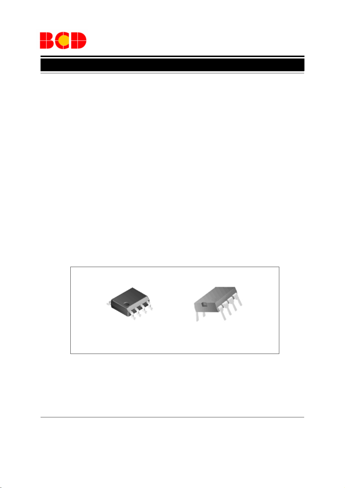
The AZ4558C is available in DIP-8 and SOIC-8 packages.
Features
· Internally Frequency Compensated
· Large Signal Voltage Gain: 100dB Typical
· Gain and Phase Match between Amplifiers
· Gain Bandwidth Product (at 10kHz): 5.5MHz
· Pin to Pin Compatible with MC1458
Applications
· Audio AC-3 Decoder System
· Audio Amplifier
SOIC-8 DIP-8
Figure 1. Package Types of AZ4558C
Jan. 2013 Rev. 1. 7 BCD Semiconductor Manufacturing Limited
1
Page 2
Data Sheet
- Input
+ Input
V
EE
Output
V
CC
1
2
3
4
8
7
6
5
1
2
3
4
8
7
6
5
DUAL BIPOLAR OPERATIONAL AMPLIFIERS AZ4558C
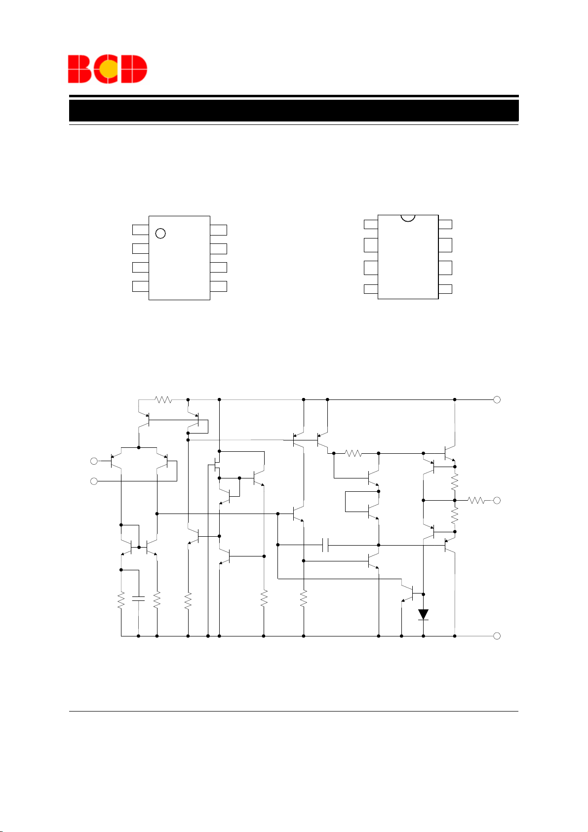
Pin Configuration
M Package
(SOIC-8)
OUTPUT 1
INPUT 1-
INPUT 1+
V
EE
Figure 2. Pin Configuration of AZ4558C (Top View)
Functional Block Diagram
V
CC
OUTPUT 2
INPUT 2-
INPUT 2+
OUTPUT 1
INPUT 1-
INPUT 1+
V
EE
P Package
(DIP-8)
V
CC
OUTPUT 2
INPUT 2-
INPUT 2+
Figure 3. Functional Block Diagram of AZ4558C (Each Amplifier)
Jan. 2013 Rev. 1. 7 BCD Semiconductor Manufacturing Limited
2
Page 3
Data Sheet
DUAL BIPOLAR OPERATIONAL AMPLIFIERS AZ4558C
Ordering Information
AZ4558C -
E1: Lead Free
G1: Green
TR: Tape and Reel
Blank: Tube
Packing
Typ e
Package
SOIC-8
DIP-8
Circuit Type
Package
M: SOIC-8
P: DIP-8
Te mp er a tu re
Range
o
-40 to 85
-40 to 85
C
o
C
Part Number Marking ID
Lead Free Green Lead Free Green
AZ4558CM-E1 AZ4558CM-G1 4558CM-E1 4558CM-G1 Tube
AZ4558CMTR-E1 AZ4558CMTR-G1 4558CM-E1 4558CM-G1 Tape & Reel
AZ4558CP-E1 AZ4558CP-G1 AZ4558CP-E1 AZ4558CP-G1 Tube
BCD Semiconductor's Pb-free products, as designated with "E1" suffix in the part number, are RoHS compliant. Products with
"G1" suffix are available in green packages.
Absolute Maximum Ratings (Note 1)
Parameter Symbol Value Unit
Supply Voltage
V
Input Voltage
V
Differential Input Voltage
V
Operating Junction Temperature T
Storage Temperature Range T
Lead Temperature (Soldering 10s) T
Power Dissipation P
CC
EE
V
ID
STG
L
D
I
J
DIP 800 mW
SOIC 500 mW
+20
-20
±15 V
±30 V
150
-65 to 150
260
V
o
C
o
C
o
C
Note 1: Stresses greater than those listed under "Absolute Maximum Ratings" may cause permanent damage to the device.
These are stress ratings only, and functional operation of the device at these or any other conditions beyond those indicated
under "Recommended Operating Conditions" is not implied. Exposure to "Absolute Maximum Ratings" for extended periods
may affect device reliability.
Recommended Operating Conditions
Parameter Min Max Unit
Supply Voltage ±2 ±18 V
Operating Temperature Range
-40
85
Jan. 2013 Rev. 1. 7 BCD Semiconductor Manufacturing Limited
3
o
C
Page 4

Data Sheet
DUAL BIPOLAR OPERATIONAL AMPLIFIERS AZ4558C
Electrical Characteristics
Operating Conditions: VCC=+15V, VEE=-15V, TA=25oC, unless otherwise specified.
Parameter Symbol Conditions Min Typ Max Unit
Input Offset Voltage
Input Offset Current
Input Bias Current
Large Signal Voltage Gain
Supply Voltage Rejection Ratio SVR
Supply Current
Input Common Mode Voltage
Range
Common Mode Rejection Ratio CMRR
Output Voltage Swing
Slew Rate SR
Rise Time
Overshoot
Input Resistance
Output Resistance
V
IO
I
I
A
I
V
V
VCM=0V
IO
VCM=0V
IB
RL=2KΩ, VO=±10V
VD
≤10KΩ
R
S
All Amplifiers, No Load 2.5 4.5 mA
CC
ICM
≤10KΩ
R
S
RL≥10KΩ
O
R
≥2KΩ
L
V
=±10V, RL=2KΩ, CL=100pF, unity
I
85 100 dB
80 100 dB
±12 V
70 95 dB
±12 ±14
±10 ±13
gain
T
K
R
R
VI=±20mV, RL=2KΩ, CL=100pF, unity
R
gain
VI=±20mV, RL=2KΩ, CL=100pF, unity
OV
gain
I
O
Unity Gain Bandwidth B Gain=0dB 2.8 MHz
=±10mV, RL=2KΩ,
V
Gain Bandwidth Product GBWP
Total Harmonic Distortion Plus
Noise
THD+N
I
=100pF, f=10KHz
C
L
f=1KHz, A
=1V
V
O
=6dB, RL=10KΩ,
V
,
RMS
15mV
10 100 nA
70 400 nA
1.8 V/μs
0.3 μs
15 %
0.5 MΩ
45 Ω
5.5 MHz
0.002 %
V
Equivalent Input Noise Voltage
Density
Output Current
Thermal Resistance
(Junction to Case)
e
N
I
SINK
I
SOURCE
θ
JC
RS=100Ω, f=1KHz
V- =1 V, V+= 0V, VO=2V
V+=1V, V-= 0V, VO=2V
10
60
35
DIP-8 55
nV
----------
mA
o
C/W
Hz
SOIC-8 81
Jan. 2013 Rev. 1. 7 BCD Semiconductor Manufacturing Limited
4
Page 5

Data Sheet
-40.0 -20.0 0.0 20.0 40.0 60.0 80.0 100.0 120.0
2.0
2.2
2.4
2.6
2.8
3.0
3.2
Supply Current (mA)
Temperature (OC)
1 10 100 1k 10k 100k 1M 10M
0
20
40
60
80
100
120
Open Loop Gain (dB)
Frequency (Hz)
1 10 100 1k 10k 100k 1M
5
10
15
20
VCC=+15V, VEE=-15V,
R
L
=2kΩ, THD+N<5%
Maximum Swing Voltage (V)
Frequency (Hz)
100 1k 10k
-16
-12
-8
-4
0
4
8
12
16
Negative Voltage Swing
Output Voltage Swing (V)
Resistance Load (Ω)
Positive Voltage Swing
DUAL BIPOLAR OPERATIONAL AMPLIFIERS AZ4558C
Typical Performance Characteristics
Figure 4. Open Loop Voltage Gain vs. Frequency
Figure 6. Maximum Output Voltage Swing
Jan. 2013 Rev. 1. 7 BCD Semiconductor Manufacturing Limited
vs. Load Resistance
Figure 5. Maximum Output Voltage Swing vs. Frequency
Figure 7. Supply Current vs. Temperature
5
Page 6

Data Sheet
-40.0 -20.0 0.0 20.0 40.0 60.0 80.0 100.0 120.0
0
20
40
60
80
100
120
Input Bias Current (nA)
Temperature (OC)
-40.0 -20.0 0.0 20.0 40.0 60.0 80.0 100.0 120.0
-2
-1
0
1
2
3
4
5
Input Offset Voltage (mV)
Temperature (OC)
DUAL BIPOLAR OPERATIONAL AMPLIFIERS AZ4558C
Typical Performance Characteristics (Continued)
Figure 8. Input Offset Voltage vs. Temperature
Figure 9. Input Bias Current vs. Temperature
Jan. 2013 Rev. 1. 7 BCD Semiconductor Manufacturing Limited
6
Page 7

Data Sheet
VCC=+12V
C3
0.1μF
C6
0.1μF
GND
GND
V
OUT
V
IN
R1 20K 1%
C4
22μF/25V
GND
C5
1000pF
C2
22μF/
25V
R3
3.3K 1%
R2 10K 1%
C1
150pF
+
3 (5)
-
2 (6)
8
4
OUT
1 (7)
AZ4558C
GND
GND
R4
6.8K
VEE=-12V
R5
10K
DUAL BIPOLAR OPERATIONAL AMPLIFIERS AZ4558C
Typical Application
Figure 10. Typical Application of AZ4558C in Audio 2nd Order Low Pass Filter
(fO=50.6kHz, Q=0.7015, Input impedance=10K, Gain=6dB, Group delay=4.48μs)
7
Jan. 2013 Rev. 1. 7 BCD Semiconductor Manufacturing Limited
Page 8

Data Sheet
4
°
6
°
R0.750(0.030)
0.254(0.010)TYP
0.130(0.005)MIN
8.200(0.323)
9.400(0.370)
0.204(0.008)
0.360(0.014)
7.620(0.300)TYP
4
°
6
°
5°
0.700(0.028)
9.000(0.354)
9.600(0.378)
3.710(0.146)
4.310(0.170)
3.000(0.118)
3.600(0.142)
0.360(0.014)
0.560(0.022)
2.540(0.100) TYP
6.200(0.244)
6.600(0.260)
3.200(0.126)
3.600(0.142)
0.510(0.020)MIN
Φ3.000(0.118)
Depth
0.100(0.004)
0.200(0.008)
1.524(0.060) TYP
Note: Eject hole, oriented hole and mold mark is optional.
DUAL BIPOLAR OPERATIONAL AMPLIFIERS AZ4558C
Mechanical Dimensions
DIP-8 Unit: mm(inch)
Jan. 2013 Rev. 1. 7 BCD Semiconductor Manufacturing Limited
8
Page 9

Data Sheet
0
°
8
°
1°
5°
R
0
.
1
5
0
(
0
.
0
0
6
)
R0.150(0.006)
1.000(0.039)
0.330(0.013)
0.510(0.020)
1.350(0.053)
1.750(0.069)
0.100(0.004)
0.300(0.012)
0.900(0.035)
0.800(0.031)
0.200(0.008)
3.800(0.150)
4.000(0.157)
7
°
7
°
2
0
:
1
D
1.270(0.050)
TYP
0.190(0.007)
0.250(0.010)
8
°
D
5.800(0.228)
6.200(0.244)
0.675(0.027)
0.725(0.029)
0.320(0.013)
8
°
0.450(0.017)
0.800(0.031)
4.700(0.185)
5.100(0.201)
Note: Eject hole, oriented hole and mold mark is optional.
DUAL BIPOLAR OPERATIONAL AMPLIFIERS AZ4558C
Mechanical Dimensions (Continued)
SOIC-8 Unit: mm(inch)
φ
Jan. 2013 Rev. 1. 7 BCD Semiconductor Manufacturing Limited
9
Page 10

BCD Semiconductor Manufacturing Limited
IMPORTANT NOTICE
IMPORTANT NOTICE
BCD Semiconductor Manufacturing Limited reserves the right to make changes without further notice to any products or specifi-
BCD Semiconductor Manufacturing Limited reserves the right to make changes without further notice to any products or specifi-
cations herein. BCD Semiconductor Manufacturing Limited does not assume any responsibility for use of any its products for any
cations herein. BCD Semiconductor Manufacturing Limited does not assume any responsibility for use of any its products for any
particular purpose, nor does BCD Semiconductor Manufacturing Limited assume any liability arising out of the application or use
particular purpose, nor does BCD Semiconductor Manufacturing Limited assume any liability arising out of the application or use
of any its products or circuits. BCD Semiconductor Manufacturing Limited does not convey any license under its patent rights or
of any its products or circuits. BCD Semiconductor Manufacturing Limited does not convey any license under its patent rights or
other rights nor the rights of others.
other rights nor the rights of others.
http://www.bcdsemi.com
MAIN SITE
MAIN SITE
- Headquarters
BCD Semiconductor Manufacturing Limited
BCD Semiconductor Manufactur ing Limited
- Wafer Fab
No. 1600, Zi Xing Road, Shanghai ZiZhu Science-based Industrial Park, 200241, China
Shanghai SIM-BCD Semiconductor Manufacturing Limited
Tel: +86-21-24162266, Fax: +86-21-24162277
800, Yi Shan Road, Shanghai 200233, China
Tel: +86-21-6485 1491, Fax: +86-21-5450 0008
REGIONAL SALES OFFICE
Shenzhen Office
REGIONAL SALES OFFICE
Shanghai SIM-BCD Semiconductor Manufacturing Co., Ltd., Shenzhen Office
Shenzhen Office
Unit A Room 1203, Skyworth Bldg., Gaoxin Ave.1.S., Nanshan District, Shenzhen,
Shanghai SIM-BCD Semiconductor Manufacturing Co., Ltd. Shenzhen Office
China
Advanced Analog Circuits (Shanghai) Corporation Shenzhen Office
Tel: +86-755-8826 7951
Room E, 5F, Noble Center, No.1006, 3rd Fuzhong Road, Futian District, Shenzhen 518026, China
Fax: +86-755-8826 7865
Tel: +86-755-8826 7951
Fax: +86-755-8826 7865
- Wafer Fab
BCD Semiconductor Manufacturing Limited
Shanghai SIM-BCD Semiconductor Manufacturing Co., Ltd.
- IC Design Group
800 Yi Shan Road, Shanghai 200233, China
Advanced Analog Circuits (Shanghai) Corporation
Tel: +86-21-6485 1491, Fax: +86-21-5450 0008
8F, Zone B, 900, Yi Shan Road, Shanghai 200233, China
Tel: +86-21-6495 9539, Fax: +86-21-6485 9673
Taiwan Office
BCD Semiconductor (Taiwan) Company Limited
Taiwan Office
4F, 298-1, Rui Guang Road, Nei-Hu District, Taipei,
BCD Semiconductor (Taiwan) Company Limited
Tai wan
4F, 298-1, Rui Guang Road, Nei-Hu District, Taipei,
Tel: +886-2-2656 2808
Taiwan
Fax: +886-2-2656 2806
Tel: +886-2-2656 2808
Fax: +886-2-2656 2806
USA Office
BCD Semiconductor Corp.
USA Office
30920 Huntwood Ave. Hayward,
BCD Semiconductor Corporation
CA 94544, USA
30920 Huntwood Ave. Hayward,
Tel : +1-510-324-2988
CA 94544, U.S.A
Fax: +1-510-324-2788
Tel : +1-510-324-2988
Fax: +1-510-324-2788
 Loading...