Diodes AZ4052 User Manual

Dual 4-channel Analog Multiplexer/Demultiplexer AZ4052
Preliminary Datasheet
General Description
The AZ4052 is high-speed si-gate CMOS device. The
AZ4052 is dual 4-channel analog multiplexers or
demultiplexers with common select logic. Each
multiplexer has four independent inputs/outputs (pins
nY0 to nY3) and a common input/output (pin nZ).
The common channel select logics include two digital
select inputs (pins S0 and S1) and an active LOW
enable input (pin E
four switches is selected (Low-impedance On-state)
with pins S0 and S1. When pin E
switches are in the high-impedance Off-state,
independent of pins S0 and S1. V
supply voltage pins for the digital control inputs (pins
S0, S1 and E
10V. The analog inputs/outputs (pins nY0 to nY3 and
nZ) can swing between V
V
as a negative limit. VCC-VEE may not exceed 10V.
EE
For operation as a digital multiplexer/demultiplexer,
V
is connected to GND (Typically Ground).
EE
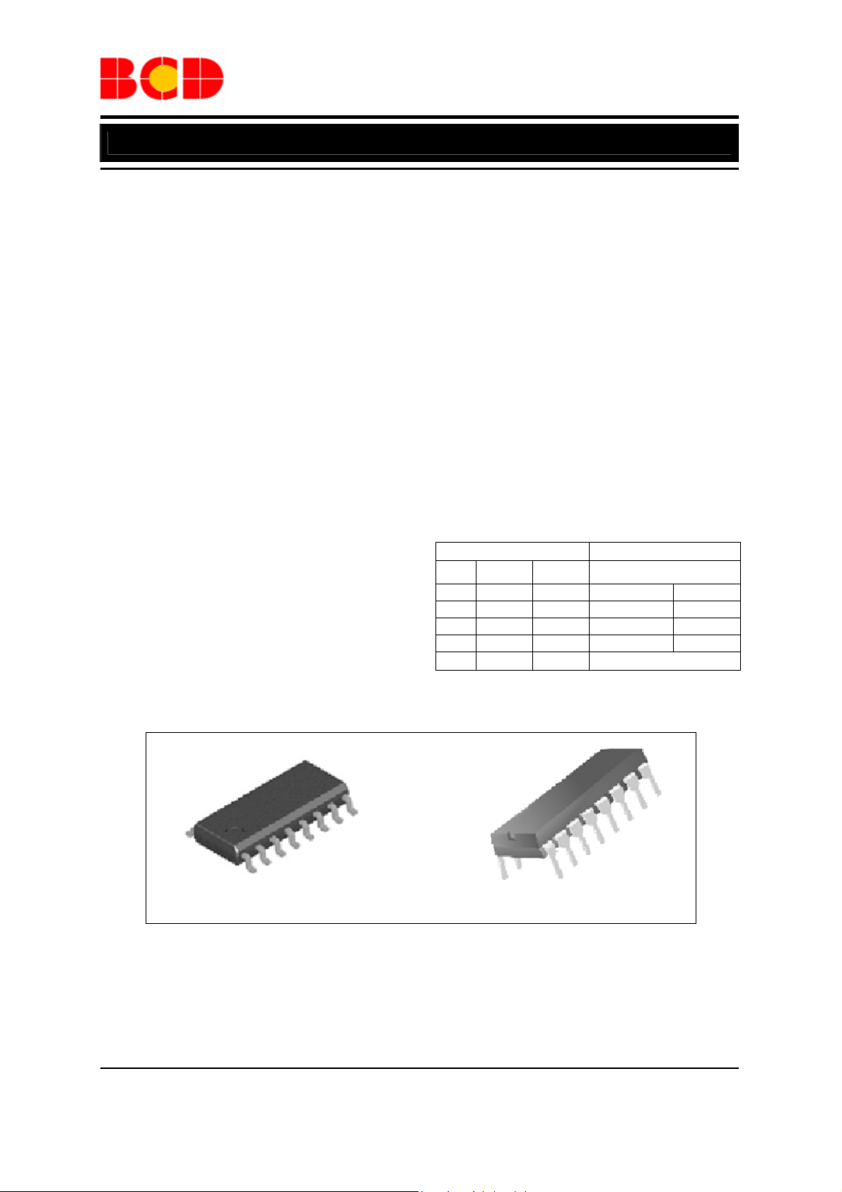
The AZ4052 is available in standard packages of
SOIC-16 and DIP-16.
___
). When pin E
___
). The VCC to GND ranges are 3.0V to
___
=LOW, one of the
___
=HIGH, all
and GND are the
CC
as a positive limit and
CC
Features
• Wide Operation Voltage: ±5.0V or 10V
• Low On-resistance:
- 55Ω (Typ.) at VCC-VEE=5V
- 40
Ω (
Typ.) at VCC-VEE=10V
• Ultra Low THD+N:
0.003% @ 10V, 0.008% @ 5.0V
• Ultra Low Crosstalk: -120dB
• Ultra Low Noise: 6.0
• Operating Temperature: -40ºC to 85ºC
μ
V
RMS
Applications
• LCD TV/PDP TV/CRT TV
• 4:1 Multi-channel Signal Selecting
Function Table
Control Input On Channel
___
E
L L L nY0 nZ
L L H nY1 nZ
L H L nY2 nZ
L H H nY3 nZ
H X X None
S1 S0
SOIC-16 DIP-16
Figure 1. Package Types of AZ4052
Oct. 2011 Rev. 1.1 BCD Semiconductor Manufacturing Limited
1

Preliminary Datasheet
Dual 4-channel Analog Multiplexer/Demultiplexer AZ4052
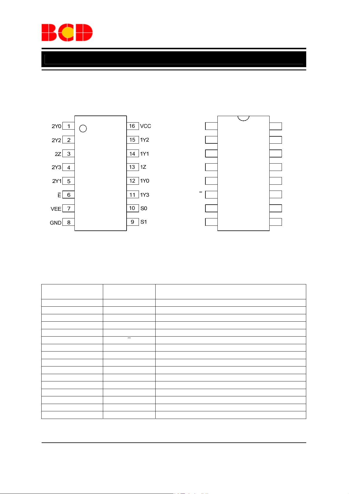
Pin Configuration
M Package P Package
(SOIC-16) (DIP-16)
VCC
2Y0
2Y2
1
2
16
15
1Y2
2Z
3
2Y3
4
2Y1
5
E
6
VEE
GND
7
8
Figure 2. Pin Configuration of AZ4052 (Top View)
Pin Descriptions
Pin Number Pin Name Function
1 2Y0 2CH signal input or output terminal 0
2 2Y2 2CH signal input or output terminal 2
3 2Z 2CH common signal input or output terminal
4 2Y3 2CH signal input or output terminal 3
5 2Y1 2CH signal input or output terminal 1
6
7 VEE Negative supply voltage
8 GND Ground (0V)
9 S1 Select logic input terminal 1
10 S0 Select logic input terminal 0
11 1Y3 1CH signal input or output terminal 3
12 1Y0 1CH signal input or output terminal 0
13 1Z 1CH common signal input or output terminal
14 1Y1 1CH signal input or output terminal 1
15 1Y2 1CH signal input or output terminal 2
16 VCC Positive supply voltage
E
Enable input (Active LOW)
14
13
12
11
10
1Y1
1Z
1Y0
1Y3
S0
S1
9
Oct. 2011 Rev. 1. 1 BCD Semiconductor Manufacturing Limited
2

Preliminary Datasheet
Dual 4-channel Analog Multiplexer/Demultiplexer AZ4052
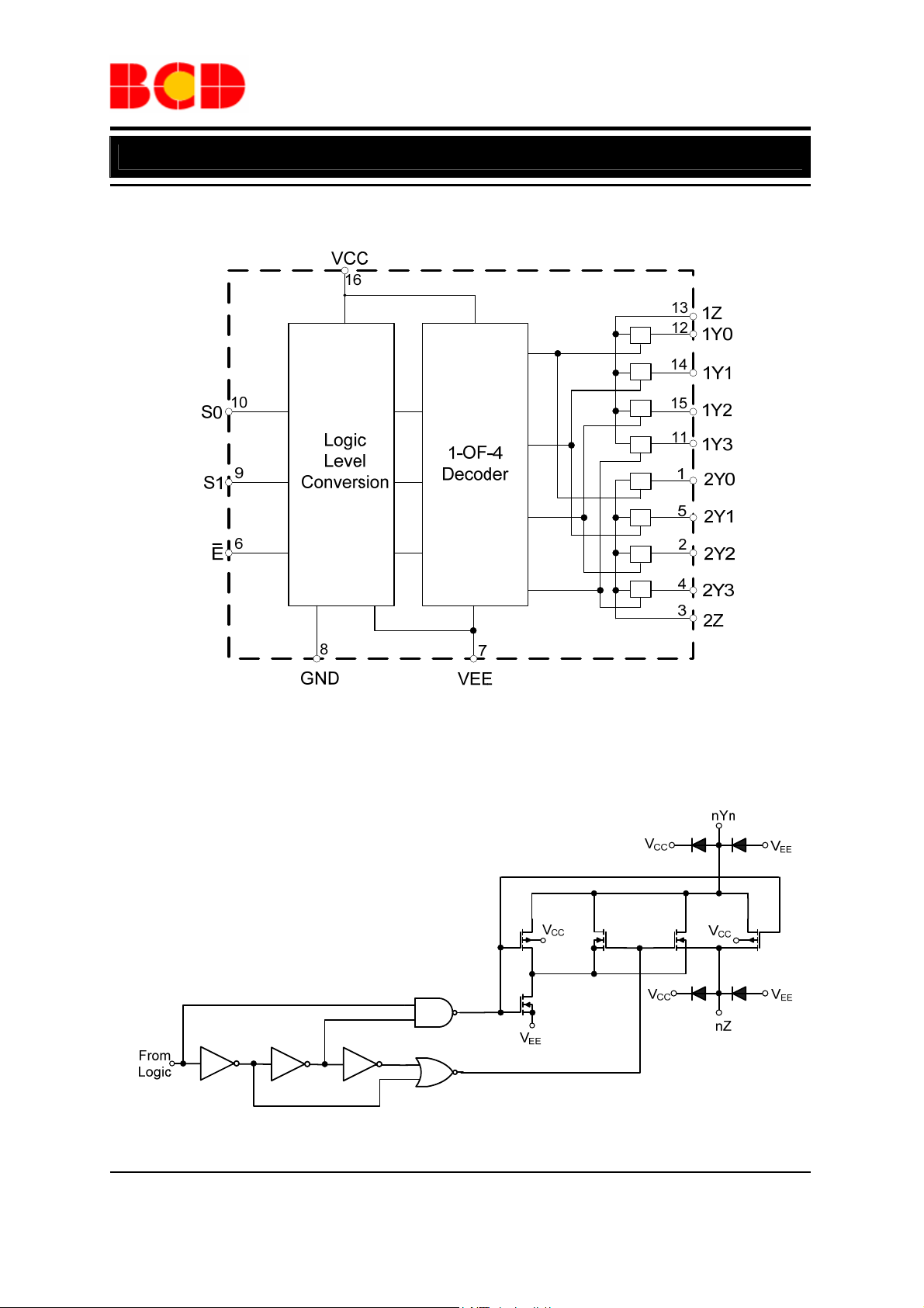
Functional Block Diagram
Figure 3. Functional Block Diagram of AZ4052
Schematic Diagram (One Switch)
Figure 4. Schematic Diagram of AZ4052
Oct. 2011 Rev. 1. 1 BCD Semiconductor Manufacturing Limited
3

Preliminary Datasheet
Dual 4-channel Analog Multiplexer/Demultiplexer AZ4052
Ordering Information
AZ4052 -
Package
SOIC-16
Circuit Type G1: Green
Package
M: SOIC-16
P: DIP-16
TR: Tape & Reel
Blank: Tube
Temperature
Range
-40 to 85°C
Part Number Marking ID
AZ4052M-G1 AZ4052M-G1 Tube
AZ4052MTR-G1 AZ4052M-G1 Tape & Reel
Packing
Type
DIP-16
-40 to 85°C
AZ4052P-G1 AZ4052P-G1 Tube
BCD Semiconductor's Pb-free products, as designated with "G1" suffix in the part number, are RoHS compliant
and Green.
Oct. 2011 Rev. 1. 1 BCD Semiconductor Manufacturing Limited
4

Preliminary Datasheet
Dual 4-channel Analog Multiplexer/Demultiplexer AZ4052
Absolute Maximum Ratings (Note 1, 2)
Parameter Symbol Condition Value Unit
Power Supply Voltage VCC -0.5 to 11.0 V
<-0.5V,
V
Input Diode Current IIK
Switch Diode Current ISK
Switch Current IS -0.5V<VS<VCC+0.5V 25 mA
V
Current IEE 20 mA
EE
V
Current
CC
GND Current
I
I
GND
CC
Power Dissipation PD
Storage Temperature Range T
Operating Junction
Temperature Range
-65 to 150 ºC
STG
150 ºC
T
J
Power Dissipation Per Switch PS 100 mW
I
V
>VCC+0.5V
I
<-0.5V,
V
S
V
>VCC+0.5V
S
50 mA
=-40ºC to 85ºC
T
A
(Note 3)
20 mA
20 mA
500 mW
ESD (Machine Model) 200 V
ESD (Human Body Model) 2000 V
Note 1: Stresses greater than those listed under “Absolute Maximum Ratings” may cause permanent damage to
the device. These are stress ratings only and functional operation of the device at these or any other conditions
beyond those indicated under “Recommended Operating Conditions” is not implied. Exposure to “Absolute
Maximum Ratings” for extended periods may affect device reliability.
Note 2: To avoid drawing V
across the bidirectional switch must not exceed 0.4V. If the switch current flows into pins nZ, no VCC current
will flow out of pins nYn. In this case there is no limit for the voltage drop across the switch, but the voltages at
pins nYn and nZ may not exceed V
Note 3: Above 70ºC derate linearly with 12mW/K (DIP-16 package).
Above 70ºC derate linearly with 8mW/K (SOIC-16 package)
current out of pins nZ, when switch current flows in pins nYn, the voltage drop
CC
or VEE.
CC
Oct. 2011 Rev. 1. 1 BCD Semiconductor Manufacturing Limited
5

Preliminary Datasheet
Dual 4-channel Analog Multiplexer/Demultiplexer AZ4052
Recommended Operating Conditions
Parameter Symbol Condition Min Typ Max Unit
Supply Voltage VIN
Logic Input Voltage VI V
Switch Signal Input/
Output Voltage
Operating Ambient
Temperature Range
Input Rise and Fall
Time
V
t
V
IS/VOS
-40 85 ºC
T
A
, tf
r
VCC-GND 3.0 10
V
3.0 10
CC-VEE
V
EE
V
EE
VCC=5.0V 6.0 400
=10V 6.0 250
V
CC
CC
CC
V
V
V
ns
Electrical Characteristics
DC Characteristics
VIS is the input voltage at pins nYn or nZ, whichever is assigned as an input; VOS is the output voltage at pins nZ
or nYn, whichever is assigned as an output, voltages are referenced to GND (Ground=0V).
Parameter Symbol
High-level
Input Voltage
V
IH
Other V
Conditions
CC
5.0 2.8
10 6.0
(V) VEE(V)
Min Typ Max Unit
V
Low-level
Input Voltage
Input Leakage
Current
Analog Switch
Off-state
Current
Analog Switch
On-state
Current
Quiescent
Supply
Current
VIL
ILI V
(Off)
I
S
I
(On)
S
I
CC
VI=VIH or VIL,
︱V
(Figure 5)
Per Channel 10 0 ±1.0
All Channels 10 0 ±2.0
V
︱VS︱=VCC-VEE
(Figure 6)
V
V
V
I=VCC
︱=VCC-V
S
or VIL,
I=VIH
I=VCC
IS=VEE
OS=VCC
or GND
EE
or GND,
or VCC,
or VEE
5.0 1.5
10 3.0
5.0 0 ±1.0
10 0 ±1.0
5.0 ±1.0
10 0 ±2.0
5.0 0 50 160
10 0 100 320
V
μA
μA
μA
μA
μA
μA
μA
μA
Oct. 2011 Rev. 1. 1 BCD Semiconductor Manufacturing Limited
6
 Loading...