

Page 1
Data Sheet
1.5A ULTRA LOW DROPOUT LINEAR REGULATOR AZ39150
General Description
The AZ39150 is low dropout three-terminal regulator
with a typical dropout of 375mV at 1.5A output current.
The AZ39150 provides current limit and thermal shutdown. On-chip thermal shutdown provides protection
against any combination of high current and ambient
temperature that would create excessive junction temperatures.
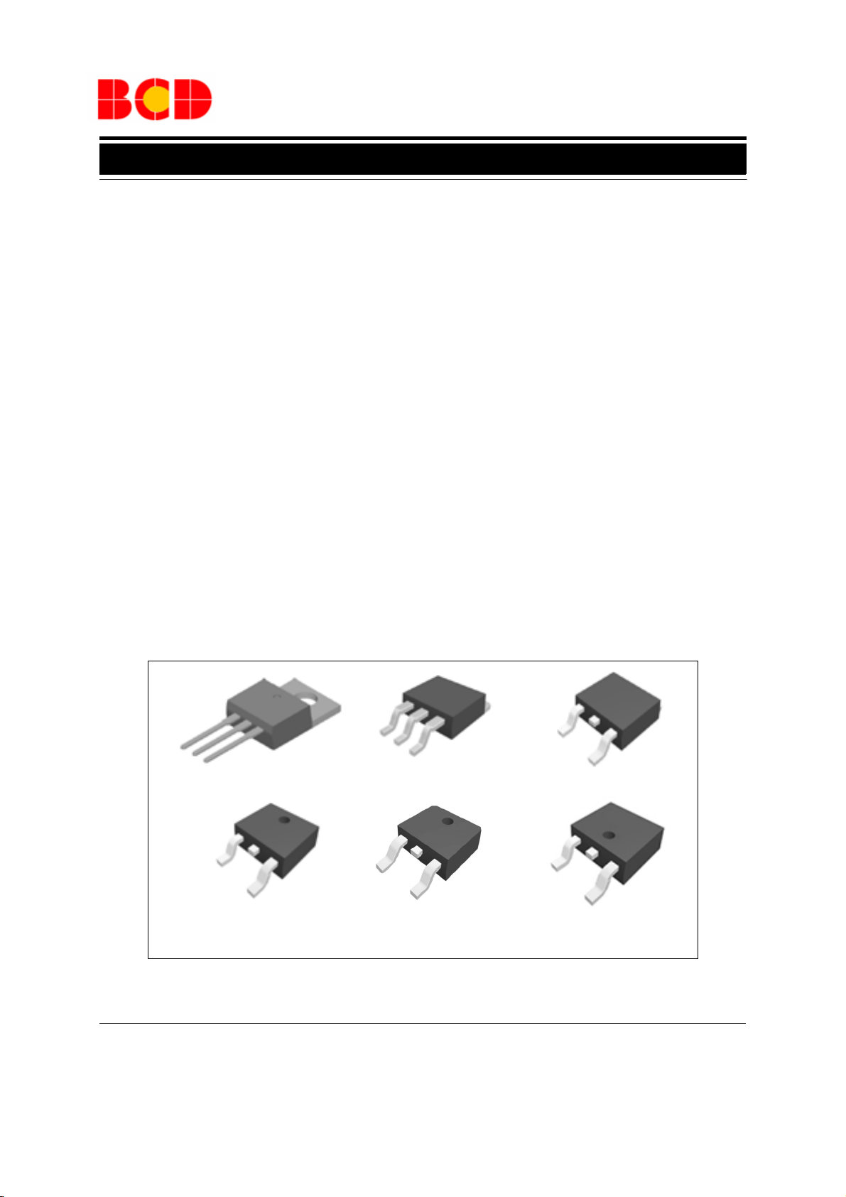
The AZ39150 is available for 3.3V, 5.0V and 12V versions now. It is available in the industry standard TO220-3, TO-263-3, TO-252-2(1), TO-252-2(2), TO252-2(3) and TO-252-2(4) power packages.
Features
· Minimum Guaranteed Output Current: 1.5A
· Dropout Voltage: 375mV at I
· Output Accuracy: 1%
· Low Ground Current
· Internal Current Limit and Thermal Protection
· Reversed-battery and Reversed-lead Insertion
Protection
· Fast Transient Response
OUT
=1.5A
Applications
· LCD TV
· Set Top Box
· LCD Monitor
· SMPS Post Regulator
· Laptop, Palmtop and Notebook
· Portable Instrumentation
· USB Power Supply
TO-220-3 TO-263-3 TO-252-2(1)
TO-252-2(2) TO-252-2(3)
Figure 1. Package Types of AZ39150
Sep. 2012 Rev. 1. 7 BCD Semiconductor Manufacturing Limited
1
TO-252-2(4)
Page 2
Data Sheet
1
2
3
1
2
3
1
2
3
1
2
3
1.5A ULTRA LOW DROPOUT LINEAR REGULATOR AZ39150
Pin Configuration
T Package
(TO-220-3)
3
2
1
(TO-252-2(1))
(TO-252-2(3))
V
OUT
GND
V
IN
V
V
OUT
GND
V
IN
DA Package
OUT
S
S/SA Package
(TO-263-3)
V
3
2
1
OUT
GND
V
IN
(TO-252-2(2))
(TO-252-2(4))
SA
V
OUT
GND
V
IN
V
OUT
3
2
1
V
IN
V
OUT
GND
GND
V
IN
GND
V
IN
Figure 2. Pin Configuration of AZ39150 (Top View)
Pin Description
Pin Number
TO-220-3/TO-263-3(S)
TO-252-2(1)/(2)/(3)/(4)
TO-263-3(SA)
13V
2 1 GND The ground pin. This pin and TAB are internally
32V
Sep. 2012 Rev. 1. 7 BCD Semiconductor Manufacturing Limited
Pin Name Function
IN
Unregulated input.
connected.
OUT
Regulated Output.
2
Page 3
Data Sheet
16V
Thermal
Shutdown
Reference
+
-
1.24V
1.5A ULTRA LOW DROPOUT LINEAR REGULATOR AZ39150
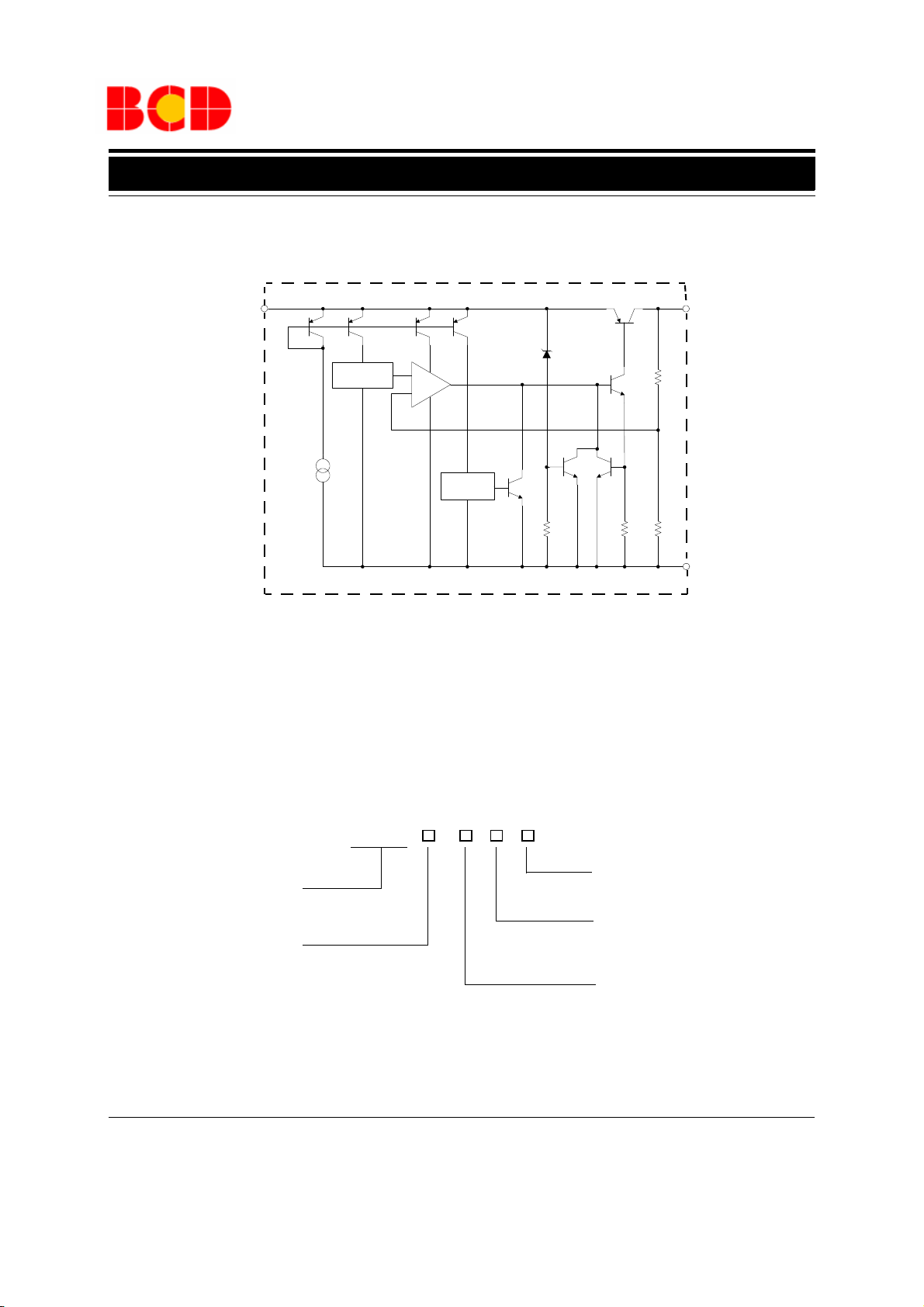
Functional Block Diagram
1(3)
V
IN
A(B)
A: TO-220-3, TO-263-3(S), TO-252-2(1)/(2)/(3)/(4)
B: TO-263-3(SA)
Figure 3. Functional Block Diagram of AZ39150
3(2)
2(1)
V
OUT
GND
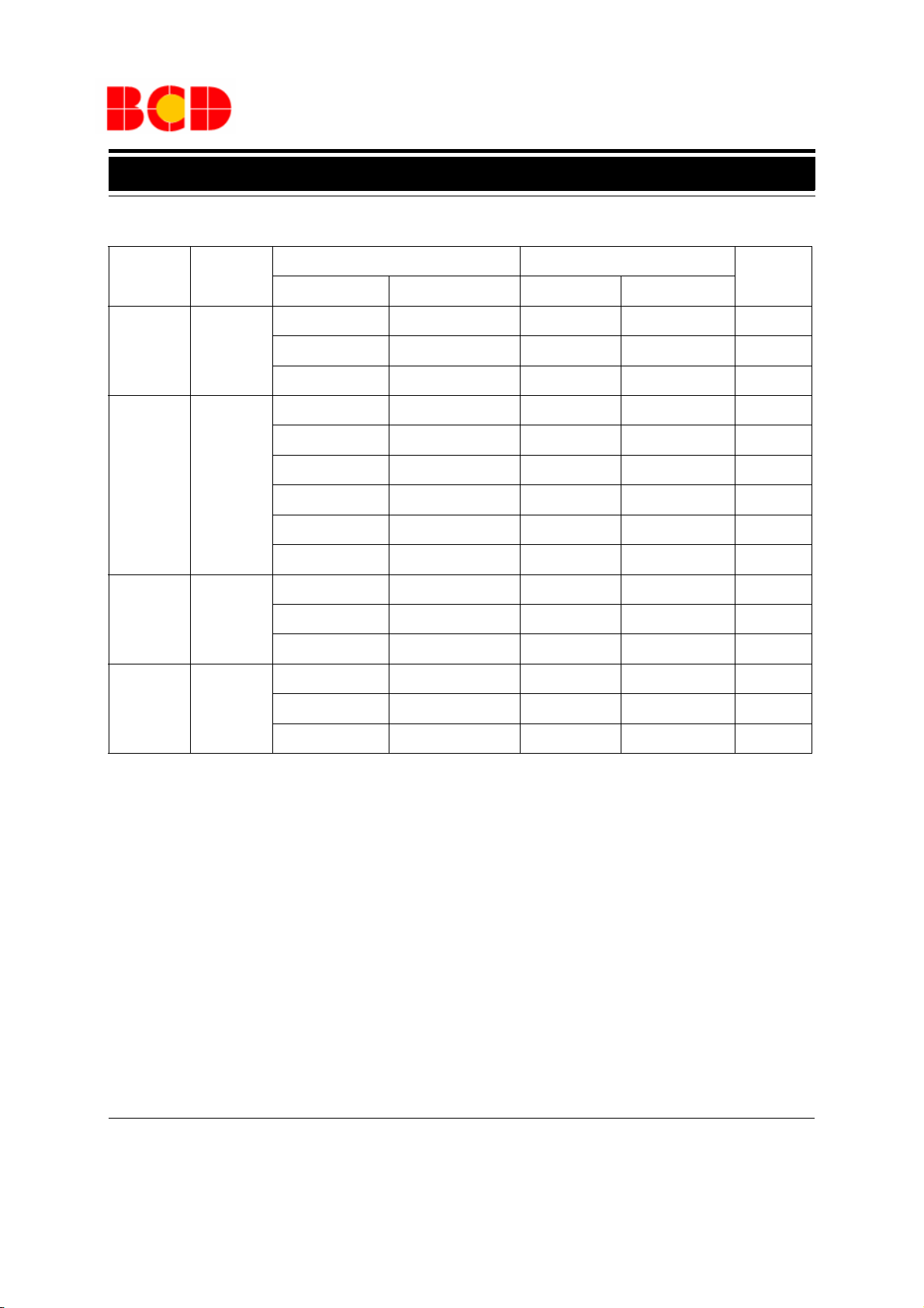
Ordering Information
-
AZ39150
Circuit Type
Package
T: TO-220-3
S: TO-263-3
SA: TO-263-3
DA: TO-252-2(1)/(2)/(3)/(4)
Sep. 2012 Rev. 1. 7 BCD Semiconductor Manufacturing Limited
E1: Lead Free
G1: Green
TR: Tape and Reel
Blank: Tube
3.3: Fixed Output 3.3V
5.0: Fixed Output 5.0V
12: Fixed Output 12V
3
Page 4
Data Sheet
1.5A ULTRA LOW DROPOUT LINEAR REGULATOR AZ39150
Ordering Information (Continued)
Package
TO-220-3
TO-263-3
(S)
TO-263-3
(SA)
TO-252-2
(1)/(2)/(3)/(4)
Te mp er a -
ture
Range
-40 to 125oC
-40 to 125
-40 to 125
-40 to 125
Part Number Marking ID Packing
Lead Free Green Lead Free Green
AZ39150T-3.3E1 AZ39150T-3.3G1 AZ39150T-3.3E1 AZ39150T-3.3G1 Tube
AZ39150T-5.0E1 AZ39150T-5.0G1 AZ39150T-5.0E1 AZ39150T-5.0G1 Tube
AZ39150T-12E1 AZ39150T-12E1 Tube
AZ39150S-3.3E1 AZ39150S-3.3G1 AZ39150S-3.3E1 AZ39150S-3.3G1 Tube
AZ39150S-3.3TRE1 AZ39150S-3.3TRG1 AZ39150S-3.3E1 AZ39150S-3.3G1 Tape & Reel
AZ39150S-5.0E1 AZ39150S-5.0G1 AZ39150S-5.0E1 AZ39150S-5.0G1 Tube
o
C
AZ39150S-5.0TRE1 AZ39150S-5.0TRG1 AZ39150S-5.0E1 AZ39150S-5.0G1 Tape & Reel
AZ39150S-12E1 AZ39150S-12E1 Tube
AZ39150S-12TRE1 AZ39150S-12E1 Tape & Reel
AZ39150SA-3.3TRG1 AZ39150SA-3.3G1 Tape & Reel
o
C
o
C
AZ39150SA-5.0TRG1 AZ39150SA-5.0G1 Tape & Reel
AZ39150SA-12TRG1 AZ39150SA-12G1 Tape & Reel
AZ39150DA-3.3TRG1 AZ39150DA-3.3G1 Tape & Reel
AZ39150DA-5.0TRG1 AZ39150DA-5.0G1 Tape & Reel
AZ39150DA-12TRG1 AZ39150DA-12G1 Tape & Reel
Typ e
BCD Semiconductor's Pb-free products, as designated with "E1" suffix in the part number, are RoHS compliant. Products with
"G1" suffix are available in green packages.
Sep. 2012 Rev. 1. 7 BCD Semiconductor Manufacturing Limited
4
Page 5
Data Sheet
1.5A ULTRA LOW DROPOUT LINEAR REGULATOR AZ39150
Absolute Maximum Ratings (Note 1)
Parameter Symbol
Supply Voltage V
Maximum Operating Junction Temperature T
Storage Temperature Range T
Lead Temperature (Soldering, 10sec) T
IN
J
STG
LEAD
Val ue
15 V
150
-65 to 150
300
Unit
o
C
o
C
o
C
ESD (Machine Model) 300 V
Note 1: Stresses greater than those listed under "Absolute Maximum Ratings" may cause permanent damage to
the device. These are stress ratings only, and functional operation of the device at these or any other conditions
beyond those indicated under "Recommended Operating Conditions" is not implied. Exposure to "Absolute Maximum Ratings" for extended periods may affect device reliability.
Recommended Operating Conditions
Parameter Symbol Min Max Unit
Supply Voltage
Operating Junction Temperature
VIN
T
J
13.2 V
-40 125
o
C
Sep. 2012 Rev. 1. 7 BCD Semiconductor Manufacturing Limited
5
Page 6
Data Sheet
1.5A ULTRA LOW DROPOUT LINEAR REGULATOR AZ39150
Electrical Characteristics
AZ39150-3.3V Electrical Characteristics
Operating Conditions: VIN=4.3V, I
Boldface applies over -40
Parameter Symbol Condition Min Typ Max Unit
Output Voltage V
Line Regulation V
Load Regulation V
Output Voltage
Temperature Coefficient
o
C≤TJ≤125oC.
ΔV
OUT
OUT
RLINE
RLOAD
/ΔTI
OUT
=10mA, C
IN=
I
=10mA 3.27 3.3 3.33 V
OUT
≤I
10mA
I
OUT
=10mA, 4.3V≤V
OUT
VIN=4.3V, 10mA≤I
=10mA 66 330
OUT
10μF, C
OUT
=10μF, T
≤1.5A, 4.3V≤VIN≤8V
≤8V
IN
≤1.5A
OUT
=25oC, unless otherwise specified. The
J
3.23 3.3 3.37 V
217mV
6.6 33 mV
μV/
o
C
Dropout Voltage (Note 2) ΔV
Ground Current I
Current Limit I
Minimum Load Current I
V
DROP
GND
LIMIT
LOAD
(MIN) 7 10 mA
Output Noise Voltage (rms) 10Hz to 100KHz, I
=1% I
OUT
I
=750mA, VIN=4.3V 4 20 mA
OUT
I
=1.5A, VIN=4.3V 17 mA
OUT
V
=0V (Note 3) 2.0 2.8 A
OUT
=10μF
C
OUT
=100mA 80 200 mV
OUT
=750mA 260 mV
I
OUT
I
=1.5A 375 500 mV
OUT
OUT
=100mA,
400 μV
Note 2: Dropout voltage is defined as the input-to-output differential when the output voltage drops to 99% of its norminal
value which is measured at V
Note 3: V
IN=VOUT(NOMINAL)
+1V applied to VIN.
OUT
+1V.
Sep. 2012 Rev. 1. 7 BCD Semiconductor Manufacturing Limited
6
Page 7

Data Sheet
1.5A ULTRA LOW DROPOUT LINEAR REGULATOR AZ39150
Electrical Characteristics (Continued)
AZ39150-5.0V Electrical Characteristics
Operating Conditions: VIN=6V, I
Boldface applies over -40
Parameter Symbol Condition Min Typ Max Unit
Output Voltage V
Line Regulation V
Load Regulation V
Output Voltage
Temperature Coefficient
o
C≤TJ≤125oC.
ΔV
OUT
OUT
RLINE
RLOAD
/ΔTI
OUT
=10mA, C
I
OUT
10mA
I
OUT
VIN=6V, 10mA≤I
OUT
IN=
10μF, C
OUT
=10μF, T
=25oC, unless otherwise specified. The
J
=10mA 4.95 5.0 5.05 V
≤I
≤1.5A, 6V≤VIN≤8V
OUT
=10mA, 6V≤V
OUT
≤8V
IN
≤1.5A
=10mA 100 500
4.90 5.0 5.10 V
325mV
10 50 mV
μV/
o
C
Dropout Voltage (Note 2) ΔV
Ground Current I
V
DROP
GND
Current Limit I
LIMIT
=1% I
OUT
I
=750mA, VIN=6V 4 20 mA
OUT
I
=1.5A, VIN=6V 17 mA
OUT
V
=0V (Note 3) 2.0 2.8 A
OUT
=100mA 80 200 mV
OUT
=750mA 260 mV
I
OUT
I
=1.5A 375 500 mV
OUT
Minimum Load Current I
Output Noise Voltage (rms) 10Hz to 100KHz, I
Note 2: Dropout voltage is defined as the input-to-output differential when the output voltage drops to 99% of its norminal
value which is measured at V
Note 3: V
IN=VOUT(NOMINAL)
OUT
(MIN) 7 10 mA
LOAD
400 μV
C
OUT
=10μF
OUT
=100mA,
+1V applied to VIN.
+1V.
Sep. 2012 Rev. 1. 7 BCD Semiconductor Manufacturing Limited
7
Page 8

Data Sheet
1.5A ULTRA LOW DROPOUT LINEAR REGULATOR AZ39150
Electrical Characteristics (Continued)
AZ39150-12V Electrical Characteristics
Operating Conditions: VIN=13V, I
Boldface applies over -40
Parameter Symbol Condition Min Typ Max Unit
Output Voltage V
Line Regulation V
Load Regulation V
Output Voltage
Temperature Coefficient
o
C≤TJ≤125oC.
ΔV
OUT
OUT
RLINE
RLOAD
/ΔTI
OUT
=10mA, C
IN=
I
=10mA 11.88 12.0 12.12 V
OUT
≤I
10mA
I
=10mA, 13V≤V
OUT
VIN=13V, 10mA≤I
=10mA 100 500
OUT
10μF, C
≤1.5A, 13V≤VIN≤15V
OUT
OUT
IN
OUT
=10μF, T
≤15V
≤1.5A
=25oC, unless otherwise specified. The
J
11.76 12.0 12.24 V
325mV
10 50 mV
μV/
o
C
Dropout Voltage (Note 2) ΔV
Ground Current I
V
DROP
GND
Current Limit I
LIMIT
=1% I
OUT
I
=750mA, VIN=13V 4 20 mA
OUT
I
=1.5A, VIN=13V 17 mA
OUT
V
=0V (Note 3) 2.0 2.8 A
OUT
=100mA 80 200 mV
OUT
=750mA 260 mV
I
OUT
I
=1.5A 375 500 mV
OUT
Minimum Load Current I
Output Noise Voltage (rms) 10Hz to 100KHz, I
Note 2: Dropout voltage is defined as the input-to-output differential when the output voltage drops to 99% of its norminal
value which is measured at V
Note 3: V
IN=VOUT(NOMINAL)
OUT
(MIN) 7 10 mA
LOAD
400 μV
C
OUT
=10μF
OUT
=100mA,
+1V applied to VIN.
+1V.
Sep. 2012 Rev. 1. 7 BCD Semiconductor Manufacturing Limited
8
Page 9

Data Sheet
0 250 500 750 1000 1250 1500
0
50
100
150
200
250
300
350
400
450
500
Dropout Voltage (mV)
Output Current (mA)
V
OUT
=5.0V
-25 0 25 50 75 100 125
0
50
100
150
200
250
300
350
400
450
500
550
600
Dropout Voltage (mV)
Temperature (oC)
I
OUT
=1.5A
V
OUT
=5.0V
0 250 500 750 1000 1250 1500
0.0
2.5
5.0
7.5
10.0
12.5
15.0
17.5
20.0
22.5
25.0
Ground Current (mA)
Output Current (mA)
VIN=6V
V
OUT
=5.0V
024681012
0.0
0.1
0.2
0.3
0.4
0.5
0.6
0.7
0.8
0.9
1.0
1.1
1.2
1.3
1.4
1.5
1.6
1.7
1.8
Ground Current (mA)
Supply Voltage (V)
V
OUT
=5.0V
I
OUT
=10mA
I
OUT
=100mA
1.5A ULTRA LOW DROPOUT LINEAR REGULATOR AZ39150
Typical Performance Characteristics
Figure 4. Dropout Voltage vs. Output Current
Figure 6. Ground Current vs. Output Current
Figure 5. Dropout Voltage vs. Temperature
Figure 7. Ground Current vs. Supply Voltage
Sep. 2012 Rev. 1. 7 BCD Semiconductor Manufacturing Limited
9
Page 10

Data Sheet
024681012
0
5
10
15
20
25
30
35
40
45
50
Ground Current (mA)
Supply Voltage (V)
V
OUT
=5.0V
I
OUT
=750mA
I
OUT
=1000mA
I
OUT
=1500mA
-25 0 25 50 75 100 125
0.27
0.28
0.29
0.30
0.31
0.32
0.33
0.34
0.35
0.36
0.37
Ground Current (mA)
Temperature (oC)
VIN=6V
V
OUT
=5.0V
I
OUT
=10mA
-25 0 25 50 75 100 125
0
1
2
3
4
5
6
7
8
Ground Current (mA)
Temperature (oC)
VIN=6V
V
OUT
=5.0V
I
OUT
=750mA
-25 0 25 50 75 100 125
10
11
12
13
14
15
16
17
18
19
20
Ground Current (mA)
Temperature (oC)
VIN=6V
V
OUT
=5.0V
I
OUT
=1.5A
1.5A ULTRA LOW DROPOUT LINEAR REGULATOR AZ39150
Typical Performance Characteristics (Continued)
Figure 8. Ground Current vs. Supply Voltage
Figure 10. Ground Current vs. Temperature
Figure 9. Ground Current vs. Temperature
Figure 11. Ground Current vs. Temperature
Sep. 2012 Rev. 1. 7 BCD Semiconductor Manufacturing Limited
10
Page 11

Data Sheet
-25 0 25 50 75 100 125
4.95
4.96
4.97
4.98
4.99
5.00
5.01
5.02
5.03
5.04
5.05
Output Voltage (V)
Temperature (oC)
VIN=6V
V
OUT
=5.0V
I
OUT
=10mA
1.5A ULTRA LOW DROPOUT LINEAR REGULATOR AZ39150
Typical Performance Characteristics (Continued)
CL=10μF
V
=5.0V
OUT
Output Voltage
Output Current
Figure 12. Output Voltage vs. Temperature
=47μF
C
L
V
OUT
Output Voltage
Output Current
Figure 14. Load Transient
=5.0V
Input Voltage Output Voltage
Figure 13. Load Transient
I
OUT
V
OUT
Figure 15. Line Transient
=10mA
=5.0V
Sep. 2012 Rev. 1. 7 BCD Semiconductor Manufacturing Limited
11
Page 12

Data Sheet
V
IN
V
OUT
GND
+
V
IN
V
OUT
AZ39150
10μF 10μF
1(3)
3(2)
2(1)
+
1.5A ULTRA LOW DROPOUT LINEAR REGULATOR AZ39150
Typical Application
A(B)
A: TO-220-3, TO-263-3(S), TO-252-2(1)/(2)/(3)/(4)
B: TO-263-3(SA)
Figure 16. Typical Application of AZ39150
Sep. 2012 Rev. 1. 7 BCD Semiconductor Manufacturing Limited
12
Page 13

Data Sheet
φ
3.560(0.140)
1
4
.
2
3
0
(
0
.
5
6
0
)
1.160(0.046)
0.813(0.032)
8
.
7
6
3
(
0
.
3
4
5
)
2.540(0.100)
0.356 (0.014)
2.080(0.082)
3
°
7
°
3.560(0.140)
7
°
9.660(0.380)
0.550(0.022)
60
°
0.381(0.015)
2
.
5
8
0
(
0
.
1
0
2
)
6
0
°
8
.
5
2
0
(
0
.
3
3
5
)
φ
1.500(0.059)
0.200(0.008)
1
.
8
5
0
(
0
.
0
7
3
)
2.540(0.100)
0.381(0.015)
0.610(0.024)
3
.
3
8
0
(
0
.
1
3
3
)
10.660(0. 420)
4.060(0.160)
1.350(0.053)
2
7
.
8
8
0
(
1
.
0
9
8
)
3
0
.
2
8
0
(
1
.
1
9
2
)
9
.
5
2
0
(
0
.
3
7
5
)
1
6
.
5
1
0
(
0
.
6
5
0
)
4.820(0.190)
2.880(0.113)
1.760(0.069)
1.5A ULTRA LOW DROPOUT LINEAR REGULATOR AZ39150
Mechanical Dimensions
TO-220-3 Unit: mm(inch)
Sep. 2012 Rev. 1. 7 BCD Semiconductor Manufacturing Limited
13
Page 14

Data Sheet
7°
3°
7°
8
.
6
4
0
(
0
.
3
4
0
)
9
.
6
5
0
(
0
.
3
8
0
)
0.990(0.039)
0.510(0.020)
2.540(0.100)
1.150(0.045)
9.650(0.380)
3°
1
4
.
7
6
0
(
0
.
5
8
1
)
8.840(0.348)
2.640(0.104)
0.020(0.001)
8
°
2
°
0°
6°
0.380(0.015)
2
.
3
9
0
(
0
.
0
9
4
)
0.360(0.014)
2
.
2
0
0
(
0
.
0
8
7
)
7
0
°
10.290(0.405)
4
.
0
7
0
(
0
.
1
6
0
)
4
.
8
2
0
(
0
.
1
9
0
)
1.390(0.055)
1.150(0.045)
1.390(0.055)
2.540(0.100)
1.270(0.050)
1.390(0.055)
2
.
6
9
0
(
0
.
1
0
6
)
1
5
.
7
4
0
(
0
.
6
2
0
)
0.250(0.010)
2.700(0.106)
0.400(0.016)
5
.
6
0
0
(
0
.
2
2
0
)
7.420(0.292)
7.980(0.314)
2.540(0.100)
2.540(0.100)
1.5A ULTRA LOW DROPOUT LINEAR REGULATOR AZ39150
Mechanical Dimensions (Continued)
TO-263-3 Unit: mm(inch)
Sep. 2012 Rev. 1. 7 BCD Semiconductor Manufacturing Limited
14
Page 15

Data Sheet
1.350(0.053)
1.650(0.065)
0.600(0.024)
0.900(0.035)
4.500(0.177)
4.700(0.185)
3°
4°
3.800REF(0.150REF)
4.800(0.189)
6.500(0.256)
4.300(0.169)
5.400(0.213)
1.400(0.055)
1.780(0.070)
0.000(0.000)
0.127(0.005)
0.450(0.018)
0.580(0.023)
2.300TYP
9.500(0.374)
9.900(0.390)
0.700(0.028)
0.900(0.035)
0.500(0.020)
0.700(0.028)
5.200(0.205)
5.400(0.213)
6.450(0.254)
6.650(0.262)
2.550(0.100)
2.900(0.114)
5.450(0.215)
6.250(0.246)
2.200(0.087)
2.400(0.094)
5°
5°
8
°
0.450(0.018)
0.580(0.023)
1.5A ULTRA LOW DROPOUT LINEAR REGULATOR AZ39150
Mechanical Dimensions (Continued)
TO-252-2(1) Unit: mm(inch)
Sep. 2012 Rev. 1. 7 BCD Semiconductor Manufacturing Limited
15
Page 16

Data Sheet
6.500(0.256)
6.700(0.264)
5.230(0.206)
5.430(0.214)
1.2±0.1
2.9REF
1.400(0.055)
1.700(0.067)
0
8
0.470(0.019)
0.600(0.024)
3
7
3
7
3
7
9.800(0.386)
10.40(0.409)
2.200(0.087)
2.380(0.094)
0.900(0.035)
1.100(0.043)
1
5
4.700REF
5.250REF
0.600(0.024)
1.000(0.039)
1.150(0.045)
1.500(0.059)
6.000(0.236)
6.200(0.244)
0.770(0.030)
0.890(0.035)
2.28BSC
0.770(0.030)
1.100(0.433)
0.900(0.035)
1.250(0.049)
1.80REF
1.5A ULTRA LOW DROPOUT LINEAR REGULATOR AZ39150
Mechanical Dimensions (Continued)
TO-252-2(2)
Unit: mm(inch)
Sep. 2012 Rev. 1. 7 BCD Semiconductor Manufacturing Limited
16
Page 17

Data Sheet
1.29±0.1
2.900REF
1.400(0.055)
1.700(0.067)
0.470(0.019)
0.600(0.024)
5
9
0
8
9.800(0.386)
10.40(0.409)
2.200(0.087)
2.380(0.094)
0.900(0.035)
1.100(0.043)
4.700REF
5.250REF
6.500(0.256)
6.700(0.264)
5.130(0.202)
5.460(0.215)
0.150(0.006)
0.750(0.030)
6.000(0.236)
6.200(0.244)
0.720(0.028)
0.850(0.033)
2.286(0.090)
BSC
0.720(0.028)
0.900(0.035)
0.900(0.035)
1.250(0.049)
1.800REF
8
0
0.600(0.024)
1.000(0.039)
7
3
9
5
1.5A ULTRA LOW DROPOUT LINEAR REGULATOR AZ39150
Mechanical Dimensions (Continued)
TO-252-2(3)
Unit: mm(inch)
17
Sep. 2012 Rev. 1. 7 BCD Semiconductor Manufacturing Limited
Page 18

Data Sheet
5.460(0.215)
4.960(0.195)
6.350(0.250)
6.730(0.265)
1.20±0.05
1.900(0.075)
1.700(0.067)
6.220(0.245)
5.970(0.235)
1.270(0.050)
0.890(0.035)
1.492(0.059)
1.145(0.045)
1.010(0.040)
1.124(0.044)
0.765(0.030)
2.290(0.090)
0.640(0.025)
0.884(0.035)
MAX
BSC
10.340(0.407)
9.940(0.391)
0.600(0.024)
0.460(0.018)
2.380(0.094)
2.180(0.086)
4.320(0.170)
MIN
MIN
5.210(0.205)
15
0
3
3
0.780(0.031)
0.650(0.026)
0.884(0.035)
0.640(0.025)
0.460(0.018)
0.610(0.024)
0.410(0.016)
0.560(0.022)
DETAIL “A”
2.160(0.085)
MIN
BASE METAL
PLATING
SECTION B-B
0.020(0.001)
0.120(0.005)
2.740(0.108)
1.500(0.059)
REF
1.780(0.070)
0
10
SEATING
PLANE
GAUGE PLANE
B
B
1.5A ULTRA LOW DROPOUT LINEAR REGULATOR AZ39150
Mechanical Dimensions (Continued)
TO-252-2(4)
Unit: mm(inch)
18
Sep. 2012 Rev. 1. 7 BCD Semiconductor Manufacturing Limited
Page 19

BCD Semiconductor Manufacturing Limited
IMPORTANT NOTICE
IMPORTANT NOTICE
BCD Semiconductor Manufacturing Limited reserves the right to make changes without further notice to any products or specifi-
BCD Semiconductor Manufacturing Limited reserves the right to make changes without further notice to any products or specifi-
cations herein. BCD Semiconductor Manufacturing Limited does not assume any responsibility for use of any its products for any
cations herein. BCD Semiconductor Manufacturing Limited does not assume any responsibility for use of any its products for any
particular purpose, nor does BCD Semiconductor Manufacturing Limited assume any liability arising out of the application or use
particular purpose, nor does BCD Semiconductor Manufacturing Limited assume any liability arising out of the application or use
of any its products or circuits. BCD Semiconductor Manufacturing Limited does not convey any license under its patent rights or
of any its products or circuits. BCD Semiconductor Manufacturing Limited does not convey any license under its patent rights or
other rights nor the rights of others.
other rights nor the rights of others.
http://www.bcdsemi.com
MAIN SITE
MAIN SITE
- Headquarters
BCD Semiconductor Manufacturing Limited
BCD Semiconductor Manufactur ing Limited
- Wafer Fab
No. 1600, Zi Xing Road, Shanghai ZiZhu Science-based Industrial Park, 200241, China
Shanghai SIM-BCD Semiconductor Manufacturing Limited
Tel: +86-21-24162266, Fax: +86-21-24162277
800, Yi Shan Road, Shanghai 200233, China
Tel: +86-21-6485 1491, Fax: +86-21-5450 0008
REGIONAL SALES OFFICE
Shenzhen Office
REGIONAL SALES OFFICE
Shanghai SIM-BCD Semiconductor Manufacturing Co., Ltd., Shenzhen Office
Shenzhen Office
Unit A Room 1203, Skyworth Bldg., Gaoxin Ave.1.S., Nanshan District, Shenzhen,
Shanghai SIM-BCD Semiconductor Manufacturing Co., Ltd. Shenzhen Office
China
Advanced Analog Circuits (Shanghai) Corporation Shenzhen Office
Tel: +86-755-8826 7951
Room E, 5F, Noble Center, No.1006, 3rd Fuzhong Road, Futian District, Shenzhen 518026, China
Fax: +86-755-8826 7865
Tel: +86-755-8826 7951
Fax: +86-755-8826 7865
- Wafer Fab
BCD Semiconductor Manufacturing Limited
Shanghai SIM-BCD Semiconductor Manufacturing Co., Ltd.
- IC Design Group
800 Yi Shan Road, Shanghai 200233, China
Advanced Analog Circuits (Shanghai) Corporation
Tel: +86-21-6485 1491, Fax: +86-21-5450 0008
8F, Zone B, 900, Yi Shan Road, Shanghai 200233, China
Tel: +86-21-6495 9539, Fax: +86-21-6485 9673
Taiwan Office
BCD Semiconductor (Taiwan) Company Limited
Taiwan Office
4F, 298-1, Rui Guang Road, Nei-Hu District, Taipei,
BCD Semiconductor (Taiwan) Company Limited
Tai wan
4F, 298-1, Rui Guang Road, Nei-Hu District, Taipei,
Tel: +886-2-2656 2808
Taiwan
Fax: +886-2-2656 2806
Tel: +886-2-2656 2808
Fax: +886-2-2656 2806
USA Office
BCD Semiconductor Corp.
USA Office
30920 Huntwood Ave. Hayward,
BCD Semiconductor Corporation
CA 94544, USA
30920 Huntwood Ave. Hayward,
Tel : +1-510-324-2988
CA 94544, U.S.A
Fax: +1-510-324-2788
Tel : +1-510-324-2988
Fax: +1-510-324-2788
 Loading...