

Page 1
Data Sheet
LOW VOLTAGE AUDIO POWER AMPLIFIER
General Description
The AZ386 is a power amplifier designed for use in
low voltage consumer applications. The gain is internally set to 20 to keep external part count low, but the
addition of an external resistor and capacitor between
pin 1 and pin 8 will increase the gain to any value from
20 to 200.
The inputs are ground referenced while the output
automatically biases to one-half the supply voltage.
The quiescent power drain is only 24mW when operating from a 5V supply, making the AZ386 ideal for
battery operation.
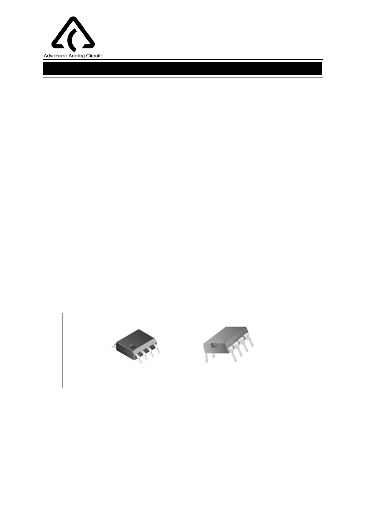
This IC is available in SOIC-8 and DIP-8 packages.
Features
· Wide Supply Voltage Range: 4V to 16V
· Low Quiescent Current Drain: 6mA
· Voltage Gains from 20 to 200
· Battery Operation
· Minimum External Parts
· Low Power Dissipation
· Low Distortion
Applications
· AM-FM Radio Amplifier
· Cordless Phone
· TV Sound Systems
· Portable Tape Player Amplifier
· Intercoms
· Line Drivers
· Ultrasonic Drivers
· Small Servo Drivers
· Power Converters
AZ386
Apr. 2007 Rev. 1. 4
SOIC-8
Figure 1. Package Types of AZ386
1
DIP-8
BCD Semiconductor Manufacturing Limited
Page 2
Data Sheet
LOW VOLTAGE AUDIO POWER AMPLIFIER
Pin Configuration
M Package/P Package
(SOIC-8/DIP-8)
GAIN
INPUT -
INPUT +
GND
Figure 2. Pin Configuration of AZ386
1
2
3
4
Top View
8
7
6
5
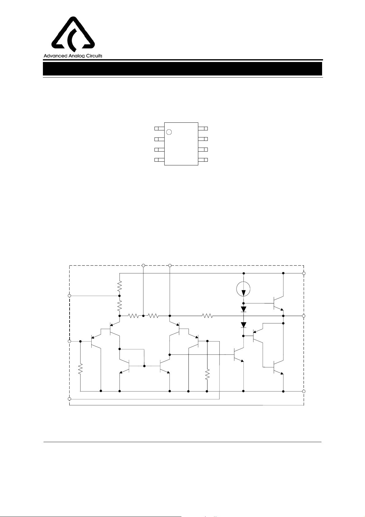
Functional Block Diagram
GAIN
BYPASS
V
CC
V
OUT
AZ386
BYPASS
INPUT -
INPUT +
GAIN
81
7
2
50KΩ
3
15KΩ
15KΩ
150Ω
1.35KΩ
GAIN
50KΩ
15KΩ
V
CC
6
5
V
OUT
4
GND
Figure 3. Functional Block Diagram of AZ386
Apr. 2007 Rev. 1. 4
BCD Semiconductor Manufacturing Limited
2
Page 3
Data Sheet
LOW VOLTAGE AUDIO POWER AMPLIFIER
Ordering Information
AZ386 -
Circuit Type
Package
M: SOIC-8
P: DIP-8
Package
SOIC-8
DIP-8
Temperature
Range
o
0 to 70
C
o
0 to 70
C
AZ386M AZ386M-E1 386M 386M-E1 Tube
AZ386MTR AZ386MTR-E1 386M 386M-E1 Tape & Reel
AZ386P AZ386P-E1 AZ386P AZ386P-E1 Tube
Part Number Marking ID
Tin Lead Lead Free Tin Lead Lead Free
AZ386
E1: Lead Free
Blank: Tin Lead
TR: Tape and Reel
Blank: Tube
Packing Type
BCD Semiconductor's Pb-free products, as designated with "E1" suffix in the part number, are RoHS compliant.
Apr. 2007 Rev. 1. 4
BCD Semiconductor Manufacturing Limited
3
Page 4
Data Sheet
LOW VOLTAGE AUDIO POWER AMPLIFIER
AZ386
Absolute Maximum Ratings (Note 1)
Parameter Symbol Value Unit
T
V
V
P
T
CC
D
IN
STG
AZ386P 1.25 W
AZ386M 0.73 W
J
Power Supply Voltage
Package Dissipation (Note 2)
Input Voltage
Junction Temperature
Storage Temperature Range
DIP-8 Soldering
Soldering Information
(10 sec.)
SOIC-8 (15 sec.) 215
Thermal Resistance
θ
JA
DIP-8 107
SOIC-8 172
Note 1: Stresses greater than those listed under "Absolute Maximum Ratings" may cause permanent damage to the
device. These are stress ratings only, and functional operation of the device at these or any other conditions beyond
those indicated under "Recommended Operating Condi tions" is not implied. Exposure to "Absolute Maximum
Ratings" for extended periods may affect device reliability.
Note 2: For operation in ambient temperatures (T
maximum junction temperature and 1) a thermal resistance of 107
o
package and 2) a thermal resistance of 172
C/W for the small outline package.
) above 25oC, the device must be derated based on a 150oC
A
o
18
-0.4 to 0.4
150
-55 to 150
260
o
o
o
o
C/W
V
V
C
C
C
C/W junction to ambient for the Dual-in-Line
Recommended Operating Conditions
Parameter Min Max Unit
Operating Temperature Range 0 70
Apr. 2007 Rev. 1. 4
BCD Semiconductor Manufacturing Limited
4
o
C
Page 5

Data Sheet
LOW VOLTAGE AUDIO POWER AMPLIFIER
AZ386
Electrical Characteristics (Note 3)
o
=25
Operating Conditions: T
Parameter Symbol Test Conditions Min Typ Max Unit
Supply Voltage V
Quiescent Current I
Output Power
Voltage Gain
Bandwidth
Total Harmonic Distortion
Power Supply Rejection Ratio PSRR
Input Resistance R
Input Bias Current I
C unless otherwise specified.
A
CC
VCC=6V, VIN=0
Q
VCC=6V, RL=8Ω, THD=10%
P
G
BW
THD
BIAS
VCC=9V, RL=8Ω, THD=10%
OUT
VCC=16V, RL=32Ω, THD=10%
VCC=6V, f=1KHz
V
10µF from Pin 1 to 8
VCC=6V, Pins 1 and 8 open
V
=6V, RL=8Ω, P
CC
f=1KHz, Pins 1 and 8 open
VCC=6V, f=1KHz, C
Pins 1 and 8 open, Referred to Output
IN
VCC=6V, Pins 2 and 3 open
OUT=
125mW
BYPASS
=10µF,
416V
68mA
250 300 mW
500 800 mW
700 1000 mW
26 dB
45 dB
500 KHz
0.27
45
%
dB
70 KΩ
10 nA
Note 3: All voltages are measured with respect to the ground pin, unless otherwise specified.
Apr. 2007 Rev. 1. 4
BCD Semiconductor Manufacturing Limited
5
Page 6

Data Sheet
LOW VOLTAGE AUDIO POWER AMPLIFIER
Typical Performance Characteristics
8
7
6
5
4
Supply Current (mA)
3
2
1
4 6 8 1012141618
Supply Voltage (V)
Figure 4. Quiescent Supply Current vs.
Supply Voltage
60
50
40
AZ386
Output Voltage (V) (peak to peak)
AZ386
16
14
12
10
8
6
4
2
0
4 5 6 7 8 9 10 11 12 13 14 15 16
Supply Voltage (V)
Figure 5. Peak-to-Peak Output Voltage
Swing vs. Supply Voltage
1.2
1.0
0.8
AZ386
=6V RL=8Ω P
V
CC
AZ386 RL=4Ω
AZ386 RL=8Ω
AZ386 RL=16Ω
AZ386 RL=32Ω
=125mW C1,8=0
OUT
30
Voltage Gain (dB)
20
10
0
100 1k 10k 100k 1M
10
9
8
7
6
5
THD (%)
4
3
2
1
0
1 10 100 1,000
V
CC
Figure 8. Distortion vs. Output Power
Apr. 2007 Rev. 1. 4
AZ386 C1,8=0
AZ386 C1,8=10u
Frequency (Hz)
AZ386
=6V RL=8Ω f=1KHz
Power Out (mW)
0.6
THD (%)
0.4
0.2
0.0
10 100 1k 10k
Frequency (Hz)
Figure 7. Distortion vs. FrequencyFigure 6. Voltage Gain vs. Frequency
2.0
1.8
1.6
1.4
1.2
1.0
0.8
Device Dissipation (W)
0.6
0.4
0.2
0.0
0.0 0.1 0.2 0.3 0.4 0.5
AZ386 VCC=12V
AZ386 VCC=9V
AZ386 VCC=6V
R
=4Ω
L
Output Power (W)
Figure 9. Device Dissipation vs. Output Power
(4Ω Load)
BCD Semiconductor Manufacturing Limited
6
Page 7

Data Sheet
LOW VOLTAGE AUDIO POWER AMPLIFIER
Typical Performance Characteristics (Continued)
2.0
1.8
1.6
1.4
1.2
1.0
0.8
Device Dissipation (W)
0.6
0.4
0.2
0.0
AZ386 VCC=16V
AZ386 VCC=12V
AZ386 VCC=9V
AZ386 VCC=6V
=8Ω
R
L
0.0 0.1 0.2 0.3 0.4 0.5 0.6 0.7 0.8 0.9 1.0
Output Power (W)
Figure 10. Device Dissipation vs. Output Power
(8Ω Load)
1.0
0.8
0.6
0.4
Device Dissipation (W)
0.2
0.0
0.00.20.40.60.81.01.21.41.61.82.0
Figure 11. Device Dissipation vs. Output Power
Output Power (W)
(16Ω Load)
AZ386 VCC=16V
AZ386 VCC=12V
AZ386 VCC=9V
AZ386 VCC=6V
=16Ω
R
L
AZ386
Typical Applications (Note 4)
V
CC
6
V
IN
10KΩ
Figure 12. Amplifier With Gain=20
Apr. 2007 Rev. 1. 4
2
-
3
+
AZ386
4
1
7
8
0.05µF
10Ω
5
250µF
+
V
CC
10µF
+
6
V
IN
10KΩ
2
-
3
+
4
AZ386
BYPASS
1
7
0.05µF
10Ω
250µF
8
+
5
Figure 13. Amplifier With Gain=200
BCD Semiconductor Manufacturing Limited
7
Page 8

Data Sheet
LOW VOLTAGE AUDIO POWER AMPLIFIER
Typical Applications (Note 4) (Continued)
V
CC
1
0.05µF
7
+
10Ω
8
10µF
5
250µF
+
ELDEMA
CF-S-2158
3V - 15mA
1.2KΩ
6
2
-
V
IN
10KΩ
AZ386
3
+
BYPASS
4
Figure 14. Amplifier With Gain=50 Figure 15. Low Distortion Power Wienbridge Oscillator
2
3
4.7KΩ
V
-
+
CC
6
AZ386
BYPASS
390Ω
1
+
10µF
7
AZ386
8
5
0.01µF
47KΩ
0.01µF
50µF
+
0.05µF
10Ω
V
O
R
L
V
CC
6
2
-
3
+
AZ386
4
1
8
5
7
10KΩ
f = 1KHz
50µF
+
30KΩ
V
O
R
L
V
IN
10KΩ
V
CC
6
2
-
3
+
4
10KΩ
8
AZ386
7
1
5
0.05µF
0.033µF
250µF
+
10Ω
0.1µF
V
O
R
L
1KΩ
Figure 16. Amplifier With Bass Boost Figure 17. Square Wave Oscillator
Note 4: The R-C series circuit from output to ground, which will make the output stable, is depended on the different capacitive load in the circuit, the correct values for the R and C can be determined through experimental methods.
Apr. 2007 Rev. 1. 4
BCD Semiconductor Manufacturing Limited
8
Page 9

Data Sheet
LOW VOLTAGE AUDIO POWER AMPLIFIER
Mechanical Dimensions
SOIC-8 Unit: mm(inch)
4.700(0.185)
5.100(0.201)
7
°
7
°
1.270(0.050)
TYP
0.100(0.004)
0.300(0.012)
1.350(0.053)
1.750(0.069)
0.675(0.027)
0.725(0.029)
AZ386
0.320(0.013)
°
8
°
8
D
0
2
D
1
:
5.800(0.228)
6.200(0.244)
φ
0.800(0.031)
0.200(0.008)
1.000(0.039)
0.330(0.013)
0.510(0.020)
Apr. 2007 Rev. 1. 4
3.800(0.150)
4.000(0.157)
0.190(0.007)
0.250(0.010)
0.900(0.035)
R0.150(0.006)
0
°
°
8
1°
5°
0.450(0.017)
0.800(0.031)
)
6
0
0
.
0
(
0
5
1
.
0
R
BCD Semiconductor Manufacturing Limited
9
Page 10

Data Sheet
LOW VOLTAGE AUDIO POWER AMPLIFIER
Mechanical Dimensions (Continued)
DIP-8
1.524(0.060) TYP
°
6
3.710(0.146)
4.310(0.170)
3.000(0.118)
3.600(0.142)
4
°
0.254(0.010)TYP
0.360(0.014)
0.560(0.022)
2.540(0.100) TYP
0.130(0.005)MIN
3.200(0.126)
3.600(0.142)
0.510(0.020)MIN
7.620(0.300)TYP
°
6
°
4
8.200(0.323)
9.400(0.370)
AZ386
Unit: mm(inch)
0.700(0.028)
5°
0.204(0.008)
0.360(0.014)
R0.750(0.030)
Φ3.000(0.118)
Depth
0.100(0.004)
0.200(0.008)
Apr. 2007 Rev. 1. 4
6.200(0.244)
6.600(0.260)
9.000(0.354)
9.400(0.370)
BCD Semiconductor Manufacturing Limited
10
Page 11

BCD Semiconductor Manufacturing Limited
http://www.bcdsemi.com
IMPORTANT NOTICE
BCD Semiconductor Manufacturing Limited reserves the right to make changes without further notice to any products or specifications herein. BCD Semiconductor Manufacturing Limited does not assume any responsibility for use of any its products for any
particular purpose, nor does BCD Semiconductor Manufacturing Limited assume any liability arising out of the application or use
of any its products or circuits. BCD Semiconductor Manufacturing Limited does not convey any license under its patent rights or
other rights nor the rights of others.
MAIN SITE
BCD Semiconductor Manufacturing Limited
- Wafer Fab
Shanghai SIM-BCD Semiconductor Manufacturing Limited
800, Yi Shan Road, Shanghai 200233, China
Tel: +86-21-6485 1491, Fax: +86-21-5450 0008
REGIONAL SALES OFFICE
Shenzhen Office
Shanghai SIM-BCD Semiconductor Manufacturing Co., Ltd. Shenzhen Office
Advanced Analog Circuits (Shanghai) Corporation Shenzhen Office
Room E, 5F, Noble Center, No.1006, 3rd Fuzhong Road, Futian District, Shenzhen 518026, China
Tel: +86-755-8826 7951
Fax: +86-755-8826 7865
BCD Semiconductor Manufacturing Limited
- IC Design Group
Advanced Analog Circuits (Shanghai) Corporation
8F, Zone B, 900, Yi Shan Road, Shanghai 200233, China
Tel: +86-21-6495 9539, Fax: +86-21-6485 9673
Taiwan Office
BCD Semiconductor (Taiwan) Company Limited
4F, 298-1, Rui Guang Road, Nei-Hu District, Taipei,
Taiwan
Tel: +886-2-2656 2808
Fax: +886-2-2656 2806
USA Office
BCD Semiconductor Corporation
30920 Huntwood Ave. Hayward,
CA 94544, U.S.A
Tel : +1-510-324-2988
Fax: +1-510-324-2788
 Loading...