Diodes AZ34063D User Manual

Data Sheet
1A STEP-DOWN/STEP-UP/INVERTING DC-DC CONVERTER AZ34063D
General Description
The AZ34063D is a monolithic switching regulator
control circuit which contains the primary functions
required for DC-DC converters. This device consists
of internal temperature compensated reference, voltage
comparator, controlled duty cycle oscillator with active
current limit circuit, driver and high current output
switch.
The AZ34063D is specifically designed as a general
DC-DC converter to be used in Step-Down, Step-Up
and Voltage-Inverting applications with a minimum
number of external components.
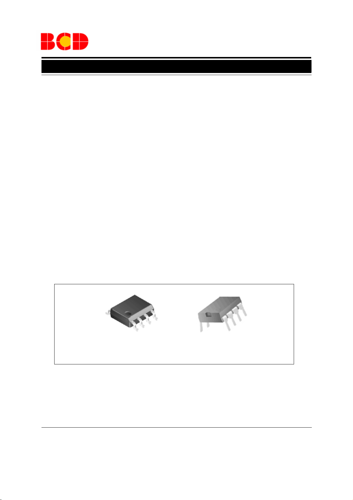
The AZ34063D is available in 2 packages: SOIC-8 and
DIP-8.
Features
• Operation from 3.0V to 36V Input
• Low Standby Current
• Current Limiting
• Output Switch Current to1A
• Output Voltage Adjustable
• Operation Frequency up to 180kHz (C
• Precision 2% Reference
Applications
· Battery Chargers
· ADSL Modems
· Hubs
· Negative Voltage Power Supplies
=100pF)
T
SOIC-8 DIP-8
Figure 1. Package Types of AZ34063D
Mar. 2010 Rev. 1. 3 BCD Semiconductor Manufacturing Limited
1

Data Sheet
1A STEP-DOWN/STEP-UP/INVERTING DC-DC CONVERTER AZ34063D
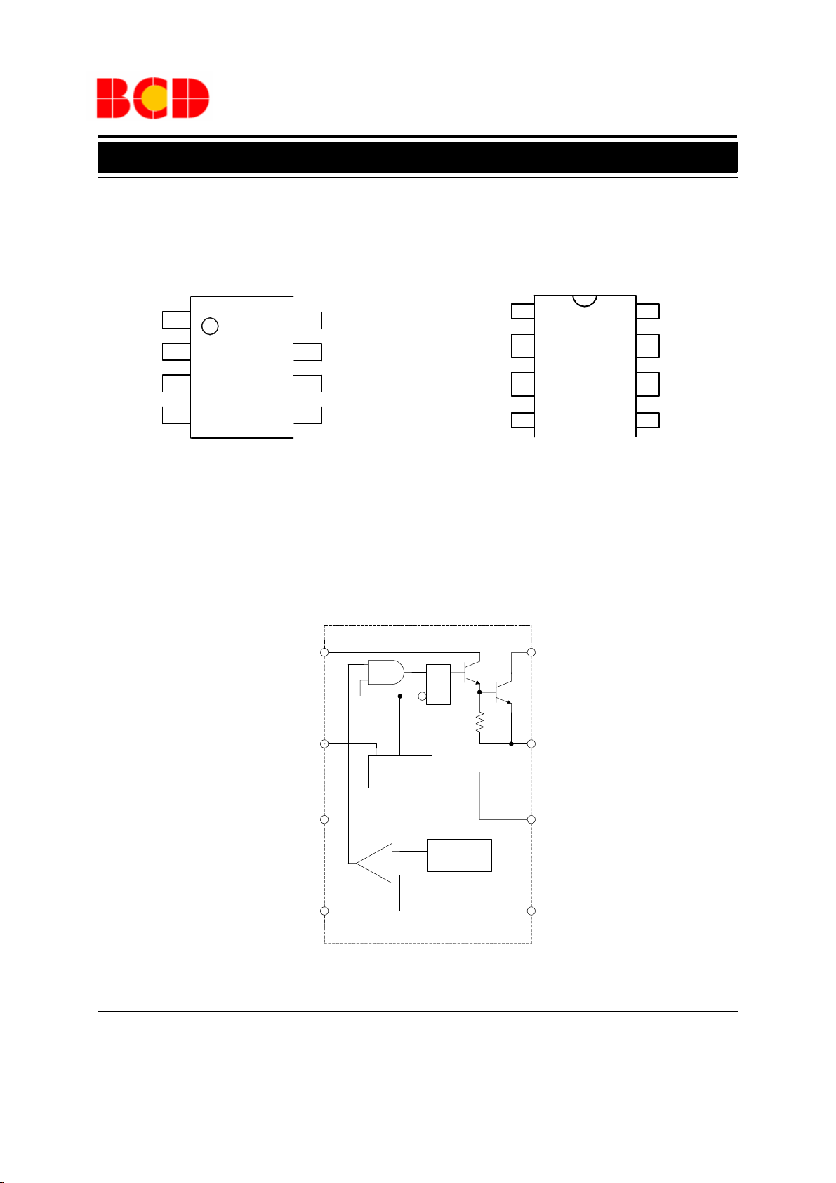
Pin Configuration
Switch
Collector
Switch
Emitter
Timing
Capacitor
GND
1
2
3
4
M Package
(SOIC-8)
Driver
8
Collector
I
7
PK
V
CC
6
Comparator
5
Inverting Input
Sense
Collector
Switch
Emitter
Timing
Capacitor
GND
Figure 2. Pin Configuration of AZ34063D (Top View)
Switch
1
2
3
4
P Package
(DIP-8)
Driver
8
Collector
I
Sense
PK
7
V
CC
6
Comparator
5
Inverting Input
Functional Block Diagram
Driver
Collector
I
Sense
PK
V
CC
Comparator
Inverting
Input
Figure 3. Functional Block Diagram of AZ34063D
8
B
A
7
SRQ
1
2
Switch
Collector
Switch
Emitter
Ipk
I
PK
C
T
OSC
6
3
Timing
Capacitor
+
-
54
1.25V
Reference
Regulator
GND
Mar. 2010 Rev. 1. 3 BCD Semiconductor Manufacturing Limited
2

Data Sheet
1A STEP-DOWN/STEP-UP/INVERTING DC-DC CONVERTER AZ34063D
Pin Description
Pin Number Pin Name Function
1 Switch Collector Internal switch transistor collector
2 Switch Emitter Internal switch transistor emitter
3 Timing Capacitor Timing Capacitor to control the switching frequency
4 GND Ground pin for all internal circuits
5 Comparator Inverting Input Inverting input pin for internal comparator
6V
7
8 Driver Collector Voltage driver collector
I
PK
CC
Sense
Voltage supply
Peak Current Sense Input by monitoring the voltage drop
across an external current sense resistor to limit the peak current through the switch
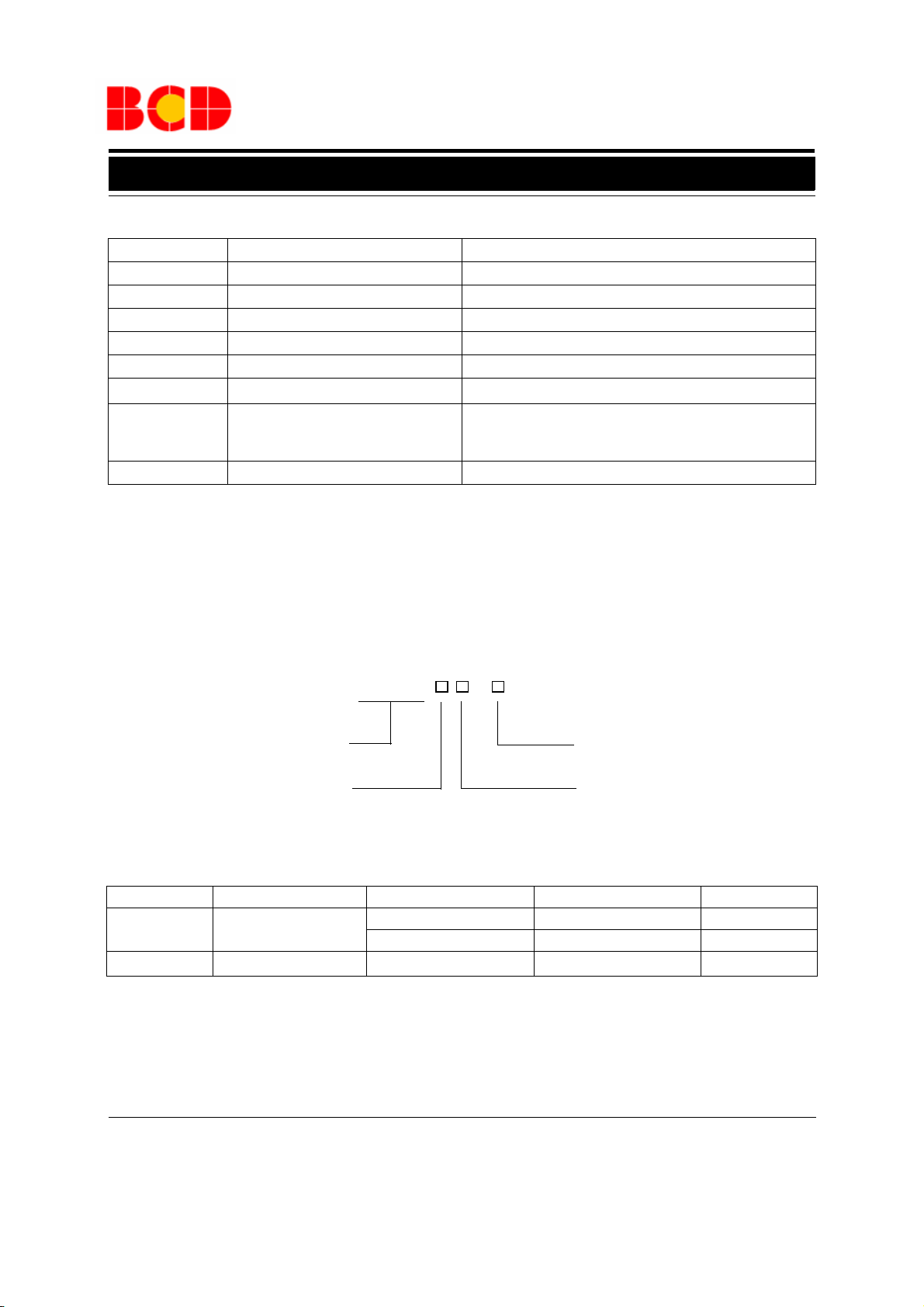
Ordering Information
AZ34063D -
Circuit Type
Package
M: SOIC-8
G1: Green
TR: Tape and Reel
Blank: Tube
P: DIP-8
Package Temperature Range Part Number Marking ID Packing Type
SOIC-8
DIP-8
BCD Semiconductor's Pb-free products, as designated with "G1" suffix in the part number, are RoHS compliant and green.
-40 to 85
-40 to 85
o
C
o
C
AZ34063DM-G1 34063DM-G1 Tube
AZ34063DMTR-G1 34063DM-G1 Tape & Reel
AZ34063DP-G1 AZ34063DP-G1
Tube
Mar. 2010 Rev. 1. 3 BCD Semiconductor Manufacturing Limited
3

Data Sheet
1A STEP-DOWN/STEP-UP/INVERTING DC-DC CONVERTER AZ34063D
Absolute Maximum Ratings (Note 1)
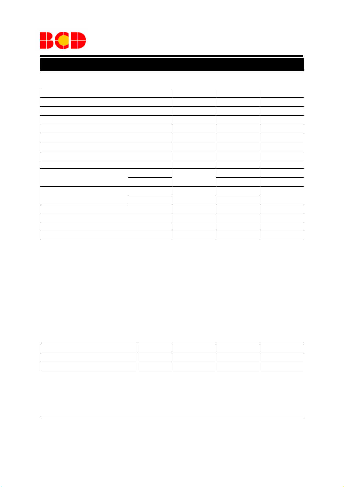
Parameter Symbol Value Unit
Power Supply Voltage V
Comparator Input Voltage Range V
Switch Collector Voltage V
Switch Emitter Voltage (V
=40V) VE(switch) 40 V
PIN 1
Switch Collector to Emitter Voltage V
Driver Collector Voltage V
Driver Collector Current (Note 2) I
Switch Current I
Power Dissipation (T
Thermal Resistance
=25oC)
A
DIP-8
SOIC-8 780 mW
DIP-8
SOIC-8 160
Operating Junction Temperature T
Lead Temperature (Soldering, 10s) T
Storage Temperature Range T
CC
IR
(switch) 40 V
C
(switch) 40 V
CE
(driver) 40 V
C
(driver) 100 mA
C
SW
P
D
θ
JA
J
LEAD
STG
ESD (Human body model) 2000 V
40 V
-0.3 to 40 V
1A
1.25 W
100
150
260
-65 to 150
o
C/W
o
o
o
C
C
C
Note 1: Stresses greater than those listed under "Absolute Maximum Ratings" may cause permanent damage to the device.
These are stress ratings only, and functional operation of the device at these or any other conditions beyond those indicated
under "Recommended Operating Conditions" is not implied. Exposure to "Absolute Maximum Ratings" for extended periods
may affect device reliability.
Note 2: Maximum package power dissipation limits must be observed.
Recommended Operating Conditions
Parameter
Supply Voltage
Ambient Temperature
Symbol
V
CC
T
A
Min Max Unit
336V
-40 85
o
C
Mar. 2010 Rev. 1. 3 BCD Semiconductor Manufacturing Limited
4

Data Sheet
1A STEP-DOWN/STEP-UP/INVERTING DC-DC CONVERTER AZ34063D
Electrical Characteristics
(V
=5.0V, TA=-40 to 85oC, unless otherwise specified.)
CC
Parameter Symbol Conditions Min Typ Max Unit
OSCILLATOR
=1.0nF 30 38 45 KHz
Frequency
Charge Current I
Discharge Current I
Discharge to Charge
Current Ratio
Current Limit Sense
Vo l t a g e
DISCHG
I
DISCHG/ICHG
V
IPK
OUTPUT SWITCH (Note 3)
Saturation Voltage,
Dalington Connection
Saturation Voltage (Note 4)
V
V
DC Current Gain h
f
OSC
CHG
(sense)
(sat)
CE
(sat)
CE
FE
V
=0V,
PIN5
T
=25oC
A
VCC=5.0V to 36 V, TA=25oC
VCC=5.0V to 36V, TA=25oC
Pin 7 to VCC, TA=25oC
I
CHG=IDISCHG
I
=1A, Pins 1, 8 connected,
SW
Common Emitter
=1A, R
I
SW
PIN8
Forced β=20, Common Emitter
ISW=1A, VCE=5.0V, TA=25oC
C
T
=330pF 75 88 100 KHz
C
T
, TA=25oC
=82 Ω to VCC,
30 38 45 µA
180 240 290 µA
5.2 6.5 7.5
250 300 350 mV
1.0 V
0.45 V
50 75
Collector Off-State Current I
(off) VCE=36V 0.01 100 µA
C
COMPARATOR
Threshold Voltage
Threshold Voltage Line
Regulation
R
EGLINE
Input Bias Current I
V
TH
TA=25oC
T
=-40 to 85oC
A
VCC=3.0V to 36V
IB
VIN=0V -20 -400 nA
1.225 1.250 1.275
1.21 1.250 1.29
1.4 5 mV
V
TOTAL DEVICE
VCC=5.0V to 36V, CT=1.0 nF,
Supply Current
Note
3:
Low duty cycle pulse technique are used during test to maintain junction temperature as close to ambient temperature
as possible.
Note 4: If the output switch is driven into hard saturation (non-Darlington configuration) at low switch currents (≤300mA) and
high driver currents (≥30mA), it may take up to 2.0µs for it to come out of saturation. This condition will shorten the off time
at frequencies 30KHz, and is magnified at high temperatures. This condition does not occur with a Darlington configuration,
since the output switch cannot saturate. If a non-Darlington configuration is used, the following output drive condition is recommended:
I
CC
V
PIN7=VCC
V
PIN2
, V
PIN5
=GND, other pins open
> VTH,
4mA
Mar. 2010 Rev. 1. 3 BCD Semiconductor Manufacturing Limited
5
 Loading...