

Page 1
Data Sheet
1.5A STEP-DOWN/STEP-UP/INVERTING DC-DC CONVERTER AZ34063A
General Description
The AZ34063A is a monolithic switching regulator
control circuit which contains the primary functions
required for DC-DC converters. This device consists
of internal temperature compensated reference, voltage
comparator, controlled duty cycle oscillator with active
current limit circuit, driver and high current output
switch.
The AZ34063A is specifically designed as a general
DC-DC converter to be used in Step-Down, Step-Up
and Voltage-Inverting applications with a minimum
number of external components.
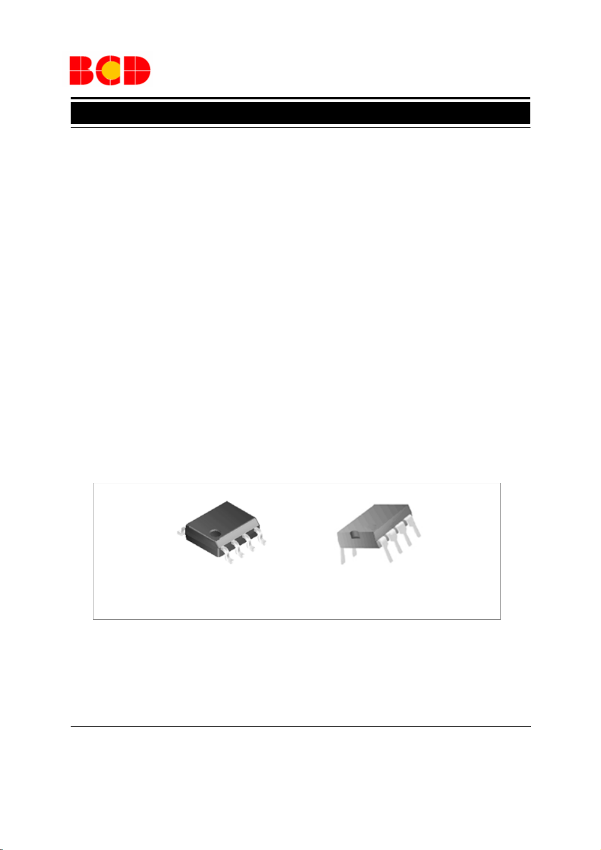
The AZ34063A is available in 2 packages: SOIC-8 and
DIP-8.
Features
• Operation from 3.0V to 36V Input
• Low Standby Current
• Current Limiting
• Output Switch Current to 1.5A
• Output Voltage Adjustable
• Operation Frequency up to 180kHz
• Precision 2% Reference
Applications
· Battery Chargers
· ADSL Modems
· Hubs
· Negative Voltage Power Supplies
SOIC-8
Figure 1. Package Types of AZ34063A
Jan. 2013 Rev. 1. 6 BCD Semiconductor Manufacturing Limited
DIP-8
1
Page 2
Data Sheet
+
-
Ipk
B
1.25V
Reference
Regulator
A
8
7
54
3
2
1
SRQ
6
I
PK
C
T
OSC
1
2
3
4
8
7
6
5
1
2
3
4
8
7
6
5
1.5A STEP-DOWN/STEP-UP/INVERTING DC-DC CONVERTER AZ34063A
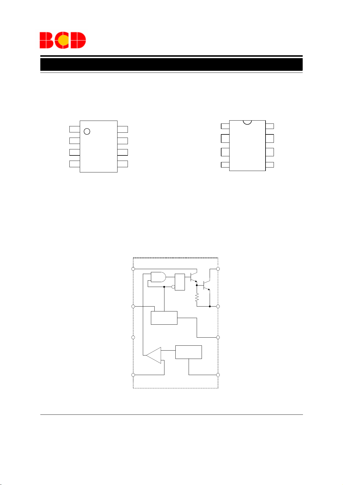
Pin Configuration
P Package
(DIP-8)
Driver
Collector
I
Sense
PK
V
CC
Comparator
Inverting Input
Switch
Collector
Switch
Emitter
Timing
Capacitor
GND
M Package
(SOIC-8)
Driver
Collector
I
Sense
PK
V
CC
Comparator
Inverting Input
Switch
Collector
Switch
Emitter
Timing
Capacitor
GND
Figure 2. Pin Configuration of AZ34063A (Top View)
Functional Block Diagram
Driver
Collector
I
Sense
PK
V
CC
Comparator
Inverting
Input
Figure 3. Functional Block Diagram of AZ34063A
Switch
Collector
Switch
Emitter
Timing
Capacitor
GND
Jan. 2013 Rev. 1. 6 BCD Semiconductor Manufacturing Limited
2
Page 3
Data Sheet
1.5A STEP-DOWN/STEP-UP/INVERTING DC-DC CONVERTER AZ34063A
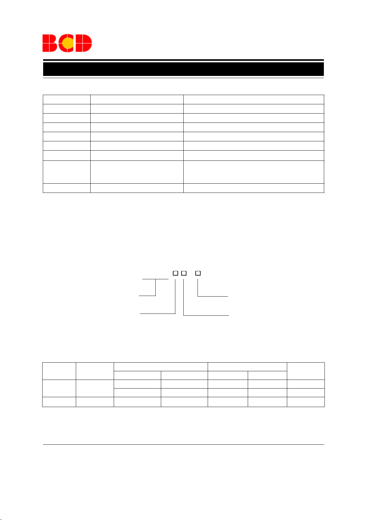
Pin Description
Pin Number Pin Name Function
1 Switch Collector Internal switch transistor collector
2 Switch Emitter Internal switch transistor emitter
3 Timing Capacitor Timing Capacitor to control the switching frequency
4 GND Ground pin for all internal circuits
5 Comparator Inverting Input Inverting input pin for internal comparator
6V
7
8 Driver Collector Voltage driver collector
I
PK
CC
Sense
Voltage supply
Peak Current Sense Input by monitoring the voltage drop
across an external current sense resistor to limit the peak current through the switch
Ordering Information
AZ34063A -
Circuit Type
Package
M: SOIC-8
E1: Lead Free
G1: Green
TR: Tape and Reel
Blank: Tube
P: DIP-8
Package
SOIC-8
DIP-8
BCD Semiconductor's Pb-free products, as designated with "E1" suffix in the part number, are RoHS compliant. Products with
"G1" suffix are available in green packages.
Temperature
Range
o
-40 to 85
-40 to 85
C
o
C
Lead Free Green Lead Free Green
AZ34063AM-E1 AZ34063AM-G1 34063AM-E1 34063AM-G1 Tube
AZ34063AMTR-E1 AZ34063AMTR-G1 34063AM-E1 34063AM-G1 Tape & Reel
AZ34063AP-E1 AZ34063AP-G1 AZ34063AP-E1 AZ34063AP-G1
Part Number Marking ID
Packing Type
Tube
Jan. 2013 Rev. 1. 6 BCD Semiconductor Manufacturing Limited
3
Page 4
Data Sheet
1.5A STEP-DOWN/STEP-UP/INVERTING DC-DC CONVERTER AZ34063A
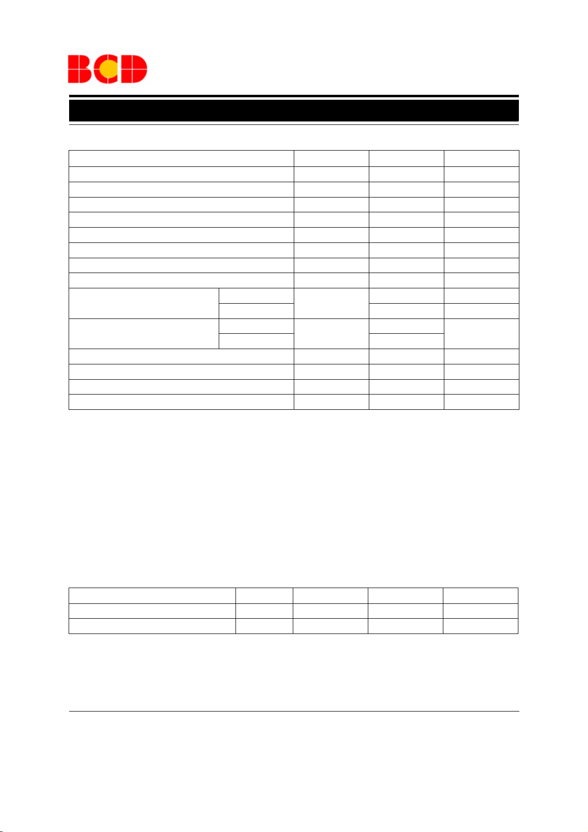
Absolute Maximum Ratings (Note 1)
Parameter Symbol Value Unit
Power Supply Voltage V
Comparator Input Voltage Range V
Switch Collector Voltage V
Switch Emitter Voltage (V
=40V) VE(switch) 40 V
PIN 1
Switch Collector to Emitter Voltage V
Driver Collector Voltage V
Driver Collector Current (Note 2) I
Switch Current I
Power Dissipation (T
Thermal Resistance
=25 ℃ )
A
DIP-8
SOIC-8 780 mW
DIP-8
SOIC-8 160
Operating Junction Temperature T
Lead Temperature (Soldering, 10s) T
Storage Temperature Range T
CC
IR
(switch) 40 V
C
(switch) 40 V
CE
(driver) 40 V
C
(driver) 100 mA
C
SW
P
D
R
θJA
J
LEAD
STG
ESD (Human body model) 2000 V
40 V
-0.3 to 40 V
1.5 A
1.25 W
100
℃ /W
150
260
-65 to 150
℃
℃
℃
Note 1: Stresses greater than those listed under "Absolute Maximum Ratings" may cause permanent damage to the device.
These are stress ratings only, and functional operation of the device at these or any other conditions beyond those indicated
under "Recommended Operating Conditions" is not implied. Exposure to "Absolute Maximum Ratings" for extended periods
may affect device reliability.
Note 2: Maximum package power dissipation limits must be observed.
Recommended Operating Conditions
Parameter
Supply Voltage
Ambient Temperature
Symbol
V
CC
T
A
Min Max Unit
336V
-40 85
o
C
Jan. 2013 Rev. 1. 6 BCD Semiconductor Manufacturing Limited
4
Page 5

Data Sheet
1.5A STEP-DOWN/STEP-UP/INVERTING DC-DC CONVERTER AZ34063A
Electrical Characteristics
(V
=5.0 V, TA=-40 to 85oC, unless otherwise specified.)
CC
Parameter Symbol Conditions Min Typ Max Unit
OSCILLATOR
V
=0V, CT=1.0nF
Frequency
Charge Current I
Discharge Current I
Discharge to Charge Current
Ratio
Current Limit Sense Voltage V
I
DISCHG/ICHG
IPK
OUTPUT SWITCH (Note 3)
Saturation Voltage,
Dalington Connection
Saturation Voltage (Note 4.)
V
V
f
OSC
CHG
DISCHG
(sense)
(sat)
CE
(sat)
CE
PIN5
T
=25oC
A
VCC=5.0V to 36V, TA=25oC
VCC=5.0V to 36V, TA=25oC
Pin 7 to VCC, TA=25oC
I
CHG=IDISCHG
=1.0A, Pins 1, 8 connected,
I
SW
, TA=25oC
Common Emitter
I
=1.0A, R
SW
=82Ω to VCC,
PIN8
Forced β=20, Common Emitter
30 38 45 KHz
30 38 45 μA
180 240 290 μA
5.2 6.5 7.5
250 300 350 mV
1.0 1.3 V
0.45 0.7 V
DC Current Gain
Collector Off-State Current I
h
FE
(off) VCE=36V 0.01 100 μA
C
ISW=1.0A, VCE=5.0V,
T
=25oC
A
50 75
COMPARATOR
1.225 1.250 1.275
1.21 1.250 1.29
1.4 5 mV
V
Threshold Voltage V
Threshold Voltage Line
Regulation
R
EGLINE
Input Bias Current I
TH
IB
TA=25oC
T
=-40 to 85oC
A
VCC=3.0V to 36V
VIN=0V -20 -400 nA
TOTAL DEVICE
VCC=5.0V to 36V, CT=1.0nF,
Supply Current I
Note
3:
Low duty cycle pulse technique are used during test to maintain junction temperature as close to ambient temperature
as possible.
Note 4: If the output switch is driven into hard saturation (non-Darlington configuration) at low switch currents (≤ 300mA) and
high driver currents (≥ 30mA), it may take up to 2.0us for it to come out of saturation. This condition will shorten the off time
at frequencies 30KHz, and is magnified at high temperatures. This condition does not occur with a Darlington configuration,
since the output switch cannot saturate. If a non-Darlington configuration is used, the following output drive condition is recommended:
CC
V
PIN7=VCC
V
PIN2
, V
PIN5
=GND, other pins open
> VTH,
4mA
Jan. 2013 Rev. 1. 6 BCD Semiconductor Manufacturing Limited
5
Page 6
Data Sheet
0.1 1 10 100
1
10
100
VCC=5.0V
V
PIN7=VCC
V
PIN5
=GND
T
A
=25OC
Frequency (KHz)
CT, Oscillator Timing Capacitor (nF)
0 5 10 15 20 25 30 35 40
0.5
1.0
1.5
2.0
2.5
3.0
3.5
CT=1.0nF
V
PIN7=VCC
V
PIN2
=GND
I
CC
. Supply Current (mA)
VCC. Supply Voltage (V)
0.1 1 10 100
1
10
100
1000
t
off
t
on
VCC=5.0V
V
PIN7=VCC
V
PIN5
=GND
T
A
=25OC
Ton-off. Output Switch On-Off Time (μs)
CT, Oscillator Timing Capacitor (nF)
1.5A STEP-DOWN/STEP-UP/INVERTING DC-DC CONVERTER AZ34063A
Electrical Characteristics (Continued)
Forced β of output switch:
* The 100Ω resistor in the emitter of the driver device requires about 7.0 mA before the output switch conducts.
IC output
ICdriver - 7.0mA*
≥ 10
Typical Performance Characteristics
. Oscillator Voltage (V)
OSC
V
V
=5.0V
CC
200mV/DIV
V
PIN7=VCC
V
=GND
PIN2
Pin 1,5,8=open
=1.0nF
C
T
T
=25oC
A
Time. 10μs/DIV
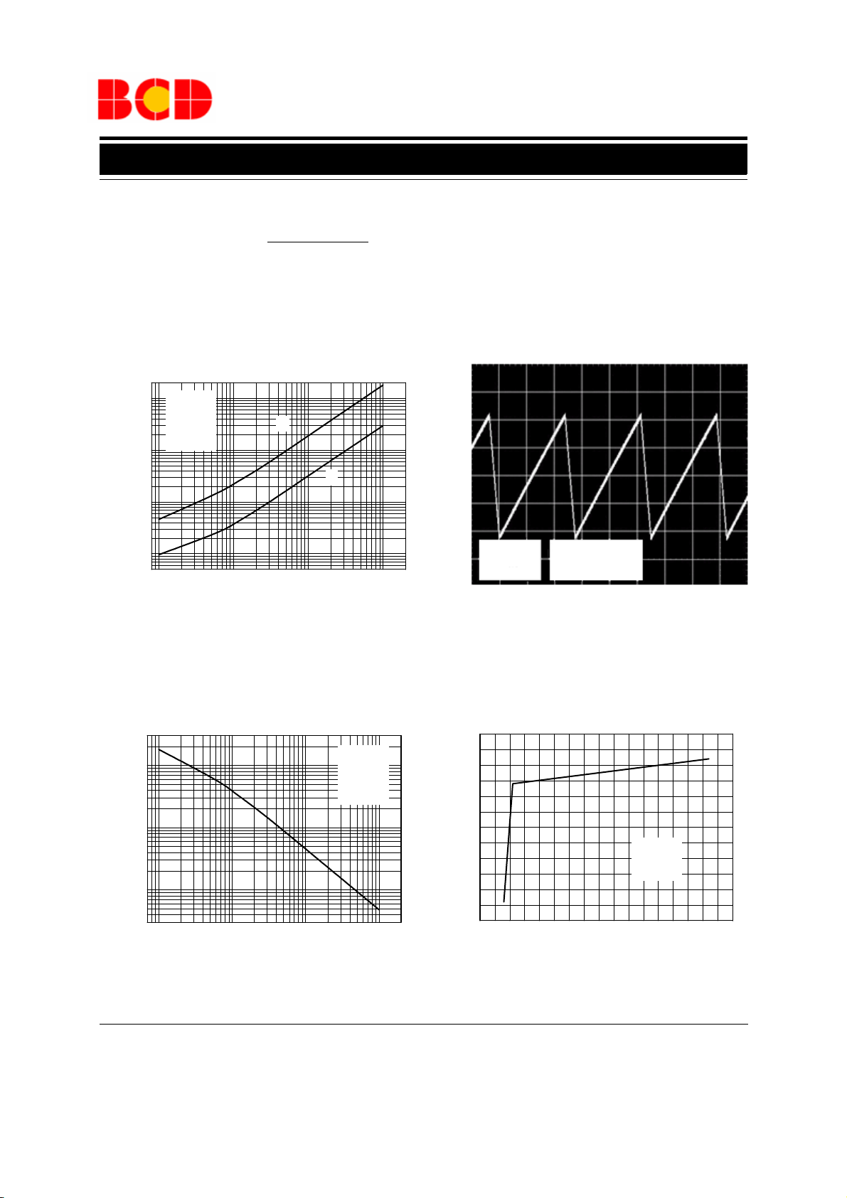
Figure 4. Output Switch On-Off Time vs. Figure 5. Timing Capacitor Waveform
Oscillator Timing Capacitor
Figure 6. Oscillator Frequency vs.Timing Capacitor Figure 7. Standard Supply Current vs. Supply Voltage
Jan. 2013 Rev. 1. 6 BCD Semiconductor Manufacturing Limited
6
Page 7
Data Sheet
-0.10.00.10.20.30.40.50.60.70.80.91.01.11.21.31.41.51.61.7
1.2
1.3
1.4
1.5
1.6
VCC=5.0V
V
PIN1,7,8=VCC
V
PIN3,5
=GND
TA=25OC
Saturation Voltage (V)
Emitter Current (A)
0.00.20.40.60.81.01.21.41.6
0.0
0.2
0.4
0.6
0.8
1.0
1.2
1.4
Darlington Connection
Forced β=20
VCC=5.0V
V
PIN7=VCC
V
PIN2,3,5
=GND
T
A
=25OC
Saturation Voltage (V)
Collector Current (A)
-60 -40 -20 0 20 40 60 80 100 120 140
240
250
260
270
280
290
300
Temperature (OC)
Current Limit Sense Voltage (mV)
1.5A STEP-DOWN/STEP-UP/INVERTING DC-DC CONVERTER AZ34063A
Typical Performance Characteristics (Continued)
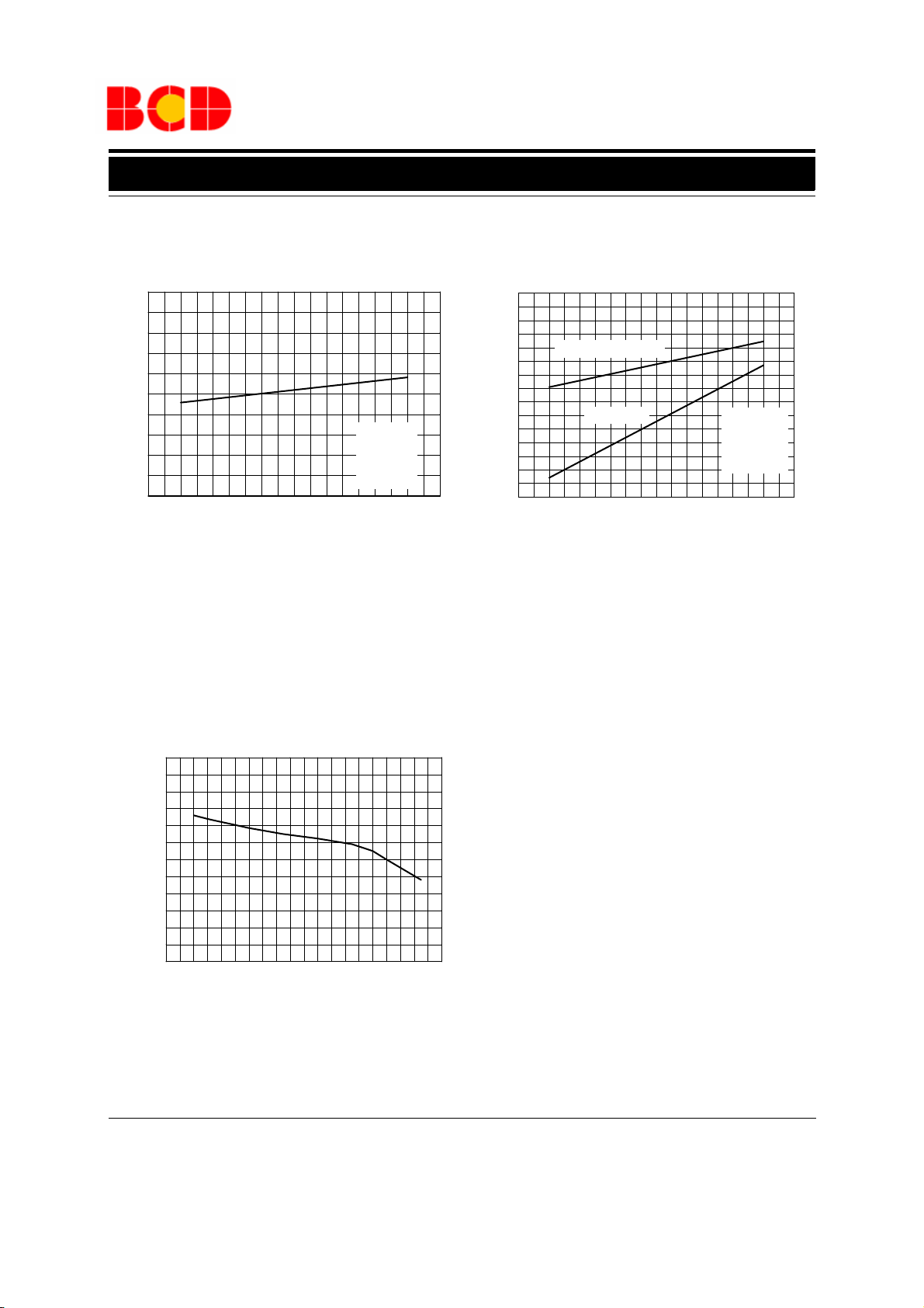
Figure 8. Emitter Follower Configuration Output
Saturation Voltage vs. Emitter current
Figure 9. Common Emitter Configuration Output Switch
Saturation Voltage vs. Collector Current
Figure 10. Current Limit Sense Voltage vs. Temperature
Jan. 2013 Rev. 1. 6 BCD Semiconductor Manufacturing Limited
7
Page 8
Data Sheet
+
-
Ipk
B
1.25V
Reference
Regulator
A
5
SRQ
I
PK
C
T
OSC
VIN 12V
C1
100μF
R3 180
C
T
470pF
L1 150μH
D1
1N5819
L2 1.0 μΗ
C3
100 μF
Optional
Filter
V
OUT
+
+
U1 AZ34063A
R1 47k
R2
2.2k
C2
330 μF
28V/175mA
+
Rsc
0.22
6
7
8
1
2
3
4
V
OUT
1.5A STEP-DOWN/STEP-UP/INVERTING DC-DC CONVERTER AZ34063A
Typical Applications
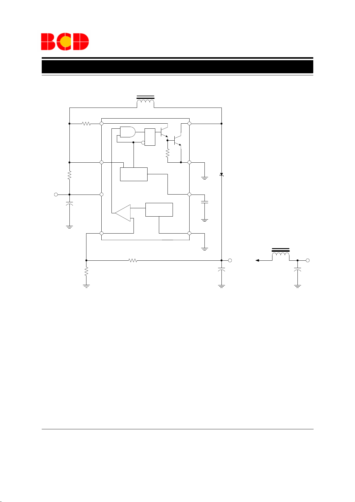
Figure 11. Step-Up Converter (Note 5)
Note 5: This is a typical step-up converter configuration. In the steady state, if the resistor divider voltage at pin
5 is greater than the voltage in the non-inverting input, which is 1.25V determined by the internal reference, the
output of the comparator will go low. At the next swithching period, the output switch will not conduct and the
output voltage will eventually drop below its nominal voltage until the divider voltage at pin 5 is lower than 1.25V.
Then the output of the comparator will go high, the output switch will be allowed to conduct. Since V
R2/(R1+R2)=1.25(V), the output voltage can be decided by V
Jan. 2013 Rev. 1. 6 BCD Semiconductor Manufacturing Limited
PIN5=VOUT
=1.25 * (R1+R2)/R2 (V).
OUT
8
*
Page 9
Data Sheet
+
-
Ipk
B
1.25V
Reference
Regulator
A
1
SRQ
I
PK
C
T
OSC
VIN 25V
C1
100μF
Rsc
0.33
L2 1.0 μH
C3
100 μF
Optional
Filter
5V/500mA
V
OUT
D1
1N5819
L1
220 μH
C
T
470 pF
+
+
R1 3.6k
R2
1.2k
C2
470 μF
+
U1 AZ34063A
2
3
4
5
6
7
8
V
OUT
1.5A STEP-DOWN/STEP-UP/INVERTING DC-DC CONVERTER AZ34063A
Typical Applications (Continued)
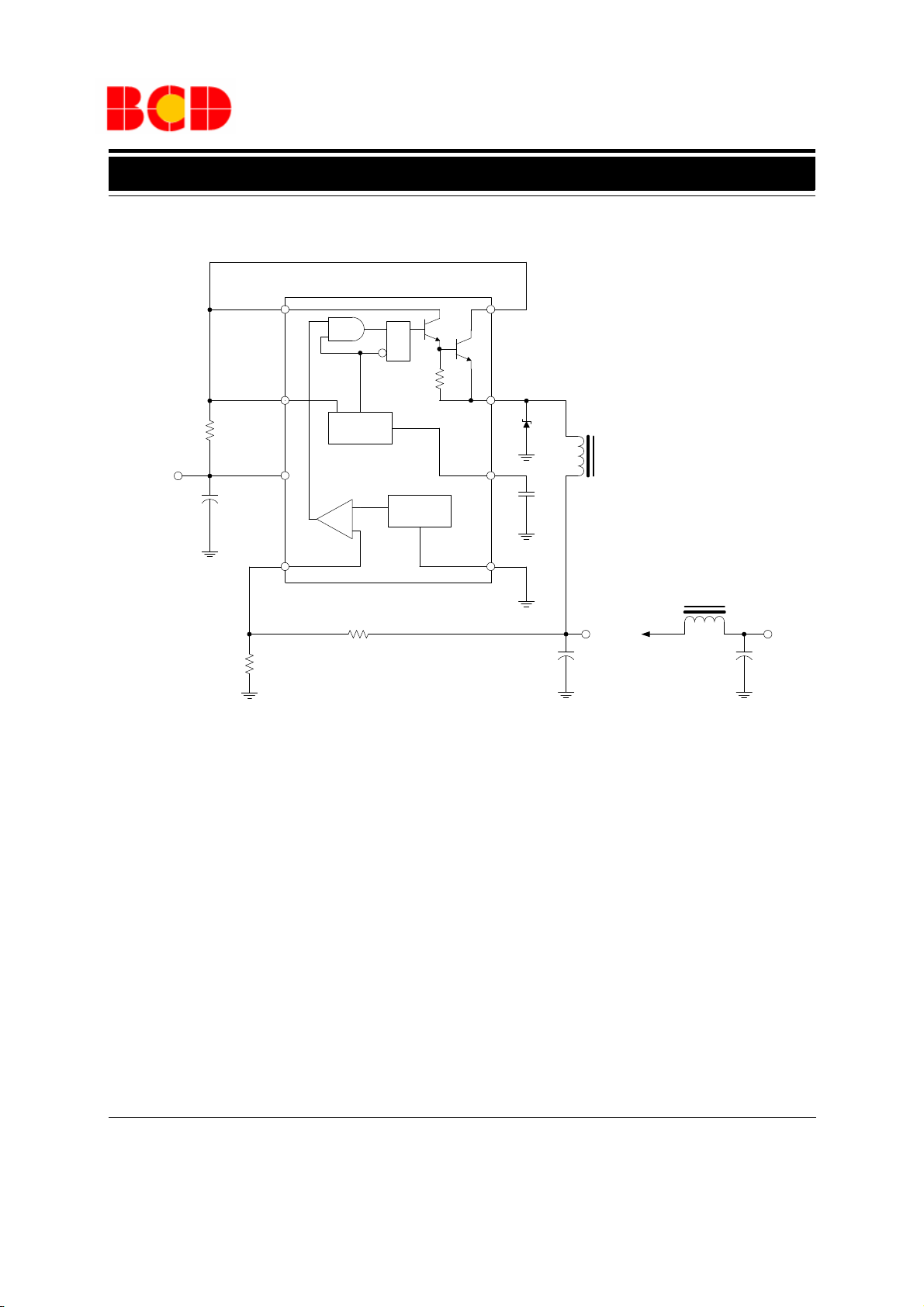
Figure 12. Step-Down converter (Note 6)
Note 6: This is a typical step-down converter configuration. The working process in the steady state is similar to
step-up converter, V
PIN5=VOUT
*R2/(R1+R2)=1.25 (V), the output voltage can be decided by V
OUT
(R1+R2)/R2 (V).
Jan. 2013 Rev. 1. 6 BCD Semiconductor Manufacturing Limited
9
=1.25*
Page 10
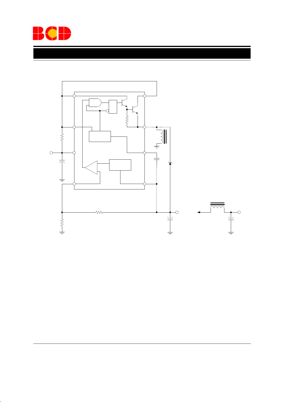
Data Sheet
+
-
Ipk
B
1.25V
Reference
Regulator
A
8
SRQ
I
PK
C
T
OSC
V
IN
4.5-6V
C1
100 μF
Rsc
0.24
L2 1.0 μΗ
Optional
Filter
V
OUT
D1
1N5819
L1
88 μΗ
+
C3
100 μF
+
C
T
470pF
R1 953
R2
8.2k
C2
1000 μF
-12V/100mA
+
U1 AZ34063A
7
6
54
3
2
1
V
OUT
1.5A STEP-DOWN/STEP-UP/INVERTING DC-DC CONVERTER AZ34063A
Typical Applications (Continued)
Figure 13. Voltage Inverting Converter (Note 7)
Note 7: This is a typical inverting converter configuration. The working process in the steady state is similar to
step-up converter, the difference in this situation is that the voltage at the non-inverting pin of the comparator is
equal to 1.25V+V
V
=-1.25*(R1+R2)/R1 (V).
OUT
OUT
, then V
Jan. 2013 Rev. 1. 6 BCD Semiconductor Manufacturing Limited
PIN5=VOUT
*R2/(R1+R2)=1.25V+V
10
, so the output voltage can be decided by
OUT
Page 11
Data Sheet
0
°
8
°
1°
5°
R
0
.
1
5
0
(
0
.
0
0
6
)
R0.150(0.006)
1.000(0.039)
0.330(0.013)
0.510(0.020)
1.350(0.053)
1.750(0.069)
0.100(0.004)
0.300(0.012)
0.900(0.035)
0.800(0.031)
0.200(0.008)
3.800(0.150)
4.000(0.157)
7
°
7
°
2
0
:
1
D
1.270(0.050)
TYP
0.190(0.007)
0.250(0.010)
8
°
D
5.800(0.228)
6.200(0.244)
0.675(0.027)
0.725(0.029)
0.320(0.013)
8
°
0.450(0.017)
0.800(0.031)
4.700(0.185)
5.100(0.201)
1.5A STEP-DOWN/STEP-UP/INVERTING DC-DC CONVERTER AZ34063A
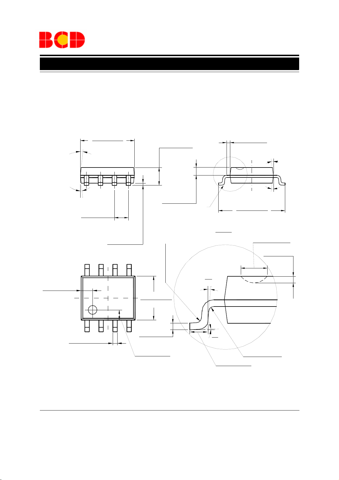
Mechanical Dimensions
SOIC-8 Unit: mm(inch)
φ
Jan. 2013 Rev. 1. 6 BCD Semiconductor Manufacturing Limited
11
Page 12

Data Sheet
4
°
6
°
R0.750(0.030)
0.254(0.010)TYP
0.130(0.005)MIN
8.200(0.323)
9.400(0.370)
0.204(0.008)
0.360(0.014)
7.620(0.300)TYP
4
°
6
°
5°
0.700(0.028)
9.000(0.354)
9.600(0.378)
3.710(0.146)
4.310(0.170)
3.000(0.118)
3.600(0.142)
0.360(0.014)
0.560(0.022)
2.540(0.100) TYP
6.200(0.244)
6.600(0.260)
3.200(0.126)
3.600(0.142)
0.510(0.020)MIN
Φ3.000(0.118)
Depth
0.100(0.004)
0.200(0.008)
1.524(0.060) TYP
Note: Eject hole, oriented hole and mold mark is optional.
1.5A STEP-DOWN/STEP-UP/INVERTING DC-DC CONVERTER AZ34063A
Mechanical Dimensions (Continued)
DIP-8 Unit: mm(inch)
Jan. 2013 Rev. 1. 6 BCD Semiconductor Manufacturing Limited
12
Page 13
BCD Semiconductor Manufacturing Limited
IMPORTANT NOTICE
IMPORTANT NOTICE
BCD Semiconductor Manufacturing Limited reserves the right to make changes without further notice to any products or specifi-
BCD Semiconductor Manufacturing Limited reserves the right to make changes without further notice to any products or specifi-
cations herein. BCD Semiconductor Manufacturing Limited does not assume any responsibility for use of any its products for any
cations herein. BCD Semiconductor Manufacturing Limited does not assume any responsibility for use of any its products for any
particular purpose, nor does BCD Semiconductor Manufacturing Limited assume any liability arising out of the application or use
particular purpose, nor does BCD Semiconductor Manufacturing Limited assume any liability arising out of the application or use
of any its products or circuits. BCD Semiconductor Manufacturing Limited does not convey any license under its patent rights or
of any its products or circuits. BCD Semiconductor Manufacturing Limited does not convey any license under its patent rights or
other rights nor the rights of others.
other rights nor the rights of others.
http://www.bcdsemi.com
MAIN SITE
MAIN SITE
- Headquarters
BCD Semiconductor Manufacturing Limited
BCD Semiconductor Manufactur ing Limited
- Wafer Fab
No. 1600, Zi Xing Road, Shanghai ZiZhu Science-based Industrial Park, 200241, China
Shanghai SIM-BCD Semiconductor Manufacturing Limited
Tel: +86-21-24162266, Fax: +86-21-24162277
800, Yi Shan Road, Shanghai 200233, China
Tel: +86-21-6485 1491, Fax: +86-21-5450 0008
REGIONAL SALES OFFICE
Shenzhen Office
REGIONAL SALES OFFICE
Shanghai SIM-BCD Semiconductor Manufacturing Co., Ltd., Shenzhen Office
Shenzhen Office
Unit A Room 1203, Skyworth Bldg., Gaoxin Ave.1.S., Nanshan District, Shenzhen,
Shanghai SIM-BCD Semiconductor Manufacturing Co., Ltd. Shenzhen Office
China
Advanced Analog Circuits (Shanghai) Corporation Shenzhen Office
Tel: +86-755-8826 7951
Room E, 5F, Noble Center, No.1006, 3rd Fuzhong Road, Futian District, Shenzhen 518026, China
Fax: +86-755-8826 7865
Tel: +86-755-8826 7951
Fax: +86-755-8826 7865
- Wafer Fab
BCD Semiconductor Manufacturing Limited
Shanghai SIM-BCD Semiconductor Manufacturing Co., Ltd.
- IC Design Group
800 Yi Shan Road, Shanghai 200233, China
Advanced Analog Circuits (Shanghai) Corporation
Tel: +86-21-6485 1491, Fax: +86-21-5450 0008
8F, Zone B, 900, Yi Shan Road, Shanghai 200233, China
Tel: +86-21-6495 9539, Fax: +86-21-6485 9673
Taiwan Office
BCD Semiconductor (Taiwan) Company Limited
Taiwan Office
4F, 298-1, Rui Guang Road, Nei-Hu District, Taipei,
BCD Semiconductor (Taiwan) Company Limited
Tai wan
4F, 298-1, Rui Guang Road, Nei-Hu District, Taipei,
Tel: +886-2-2656 2808
Taiwan
Fax: +886-2-2656 2806
Tel: +886-2-2656 2808
Fax: +886-2-2656 2806
USA Office
BCD Semiconductor Corp.
USA Office
30920 Huntwood Ave. Hayward,
BCD Semiconductor Corporation
CA 94544, USA
30920 Huntwood Ave. Hayward,
Tel : +1-510-324-2988
CA 94544, U.S.A
Fax: +1-510-324-2788
Tel : +1-510-324-2988
Fax: +1-510-324-2788
 Loading...