

Page 1
Data Sheet
3-TERMINAL 1A ADJUSTABLE VOLTAGE REGULATOR AZ317
General Description
The AZ317 is an adjustable three-terminal positive
voltage regulator with a very low dropout of 1.2V at
1A output current. Using 2 external resistors, the
AZ317 can provide an adjustable output voltage down
to 1.25V.
The AZ317 includes a circuit of trimmed bandgap reference to assure output voltage accuracy to be within
1%. It also provides current limiting and thermal shutdown. The current limit is trimmed to ensure specified
output current and controlled short-circuit current. The
On-chip thermal limiting provides protection against
any combination of overload and ambient temperature
that would create excessive junction temperature.
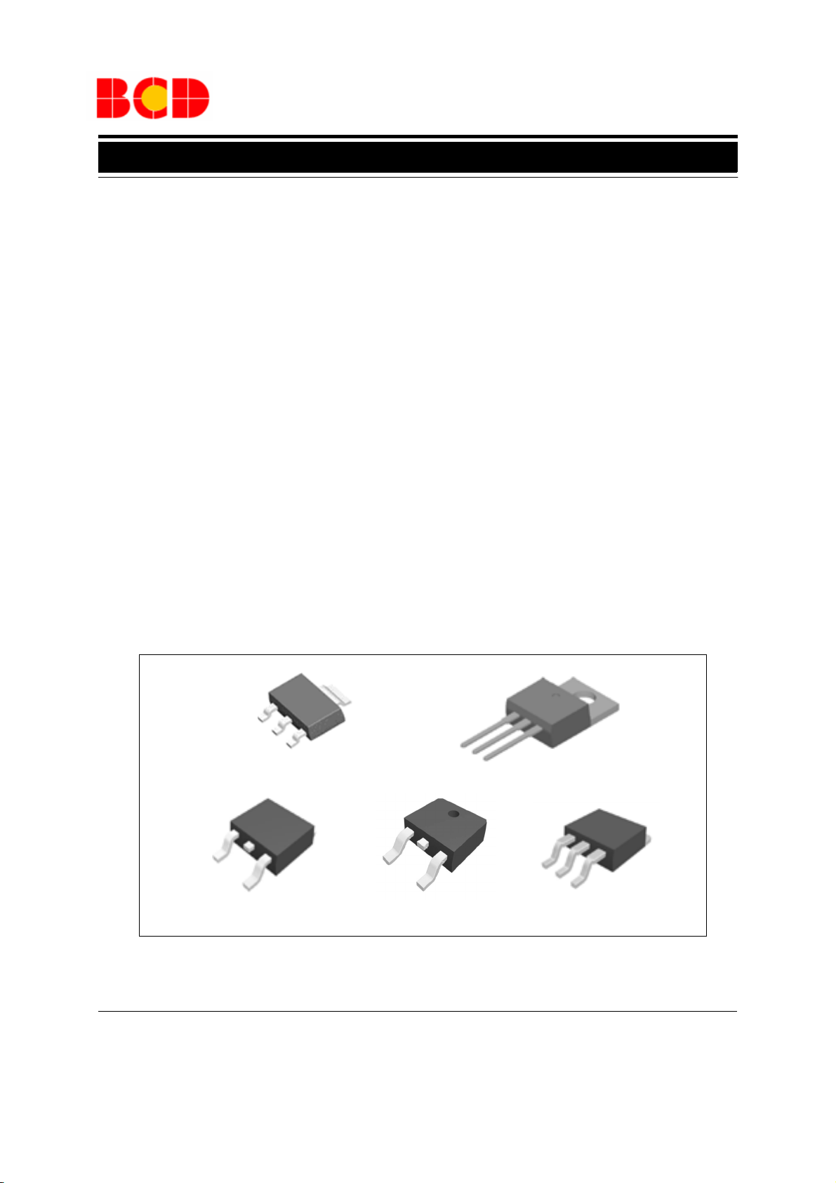
The AZ317 is available in the standard SOT-223, TO220-3, TO-252-2 (1), TO-252-2 (3) and TO-263-3
power packages.
Features
· Typical 1% Output Voltage Tolerance
· Typical 0.01%/V Line Regulation
· Typical 0.2% Load Regulation
· Very Low Dropout Voltage: 1.2V at 1A Output
Current
· Trimmed Current Limit
· On-chip Thermal Protection
o
· Operation Junction Temperature: 0 to 125
C
Applications
· PC Motherboard
· LCD Monitor
· Graphic Card
· DVD Player
· Network Interface Card/Switch
· Telecom Equipment
· Printer and other Peripheral Equipment
SOT-223
TO-252-2 (1)
Jan. 2013 Rev. 1. 6 BCD Semiconductor Manufacturing Limited
TO-252-2 (3)
Figure 1. Package Types of AZ317
TO-220-3
TO-263-3
1
Page 2
Data Sheet
Thermal
Shutdown
+
+
_
Current
Limiter
1
2
3
1
2
3
1
2
3
1
2
3
1
2
3
3-TERMINAL 1A ADJUSTABLE VOLTAGE REGULATOR AZ317
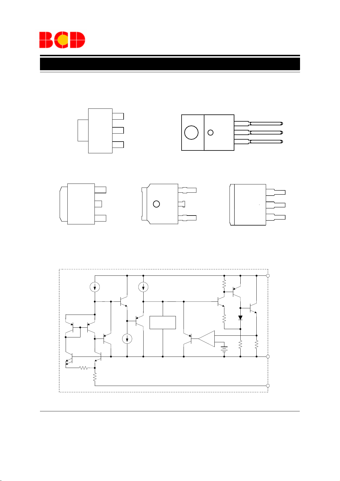
Pin Configuration
H Package
(SOT-223)
V
OUT
D Package
(TO-252-2(1))
V
OUT
T Package
(TO-220-3)
INPUT
OUTPUT
ADJ
V
OUT
(TO-252-2(3))
INPUT
OUTPUT
ADJ
Figure 2. Pin Configuration of AZ317 (Top View)
INPUT
OUTPUT
ADJ
INPUT
OUTPUT
ADJ
S Package
(TO-263-3)
INPUT
OUTPUT
ADJ
Functional Block Diagram
3
INPUT
2
OUTPUT
1
ADJ
Jan. 2013 Rev. 1. 6 BCD Semiconductor Manufacturing Limited
Figure 3. Functional Block Diagram of AZ317
2
Page 3
Data Sheet
3-TERMINAL 1A ADJUSTABLE VOLTAGE REGULATOR AZ317
Ordering Information
AZ317 -
Circuit Type
E1: Lead Free
G1: Green
Package
H: SOT-223
TR: Tape and Reel
Blank: Tube
T: TO-220-3
D: TO-252-2 (1)
/TO-252-2 (3)
S: TO-263-3
Package
SOT-223
TO-220-3
TO-252-2 (1)/
TO-252-2 (3)
TO-263-3
Temperature
Range
0 to
125oC
0 to
125oC
125oC
0 to
125oC
0 to
Lead Free Green Lead Free Green
AZ317HTR-E1 AZ317HTR-G1 EH31A GH31A Tape & Reel
AZ317T-E1 AZ317T-G1 AZ317T-E1 AZ317T-G1 Tube
AZ317DTR-E1 AZ317DTR-G1 AZ317D-E1 AZ317D-G1 Tape & Reel
AZ317S-E1 AZ317S-G1 AZ317S-E1 AZ317S-G1 Tube
AZ317STR-E1 AZ317STR-G1 AZ317S-E1 AZ317S-G1 Tape & Reel
Part Number Marking ID
BCD Semiconductor's Pb-free products, as designated with "E1" suffix in the part number, are RoHS compliant. Products with
"G1" suffix are available in green packages.
Packing
Typ e
Jan. 2013 Rev. 1. 6 BCD Semiconductor Manufacturing Limited
3
Page 4
Data Sheet
3-TERMINAL 1A ADJUSTABLE VOLTAGE REGULATOR AZ317
Absolute Maximum Ratings (Note 1)
Parameter Symbol Min Max Unit
Input Voltage V
Maximum Junction Temperature T
Storage Temperature T
Lead Temperature (Soldering, 10sec) T
LEAD
IN
J
S
150
-65 150
20 V
300
o
C
o
C
o
C
ESD (Human Body Model) ESD 4000 V
Note1: Stresses greater than those listed under "Absolute Maximum Ratings" may cause permanent damage to the
device. These are stress ratings only, and functional operation of the device at these or any other conditions beyond
those indicated under "Recommended Operating Conditions" is not implied. Exposure to "Absolute Maximum
Ratings" for extended periods may affect device reliability.
Recommended Operating Conditions
Parameter Symbol Min Max Unit
Input Voltage V
Operating Junction Temperature Range T
IN
J
V
+2 15 V
OUT
0 125
o
C
Jan. 2013 Rev. 1. 6 BCD Semiconductor Manufacturing Limited
4
Page 5
Data Sheet
3-TERMINAL 1A ADJUSTABLE VOLTAGE REGULATOR AZ317
Electrical Characteristics
(Typicals and limits apply for TJ =25oC, P≤ Maximum Power Dissipation unless otherwise specified.)(Note 2)
Parameter Symbol Conditions Min Typ Max Unit
Reference Voltage V
Line Regulation S
REF
V
Load Regulation Si V
10mA≤I
3V≤ (V
I
OUT
-V
IN
≤1A,
OUT
IN-VOUT
) ≤10V
≤ 20mA, 3V≤VIN-V
= 2V, 10mA≤I
OUT
≤10V 0.01 0.04 %/V
OUT
≤1A 0.2 0.4 %
OUT
Thermal Regulation 20ms Pulse 0.04 0.07 %/W
Dropout Voltage ΔV I
Current Limit I
LIMIT
= 1A 1.2 1.3 V
OUT
(VIN-V
) = 2V 1.2 1.5 1.8 A
OUT
Adjust Pin Current 50 100 μA
Adjust Pin Current Change 1.4V≤(V
10mA ≤I
Minimum Load Current 3V≤ (V
IN-VOUT
OUT
IN-VOUT
Ripple Rejection f =120Hz, C
(V
IN-VOUT
) ≤ 10V,
≤1A
) ≤ 15V 3.5 10 mA
=1μF Tantalum,
OUT
) = 3V, I
OUT
=1A
Temperature Stability 1%
Long -Term Stability
RMS Output Noise (% of V
Thermal Resistance,
Junction to Case
OUT
)
T
=125oC, 1000hrs
A
=25oC, 10Hz ≤ f ≤ 10kHz
T
A
SOT-223
TO-252-2 (1)/(3)
TO-220
TO-263
Thermal Shutdown Junction Temperature 150
Thermal Shutdown Hysteresis 25
1.20 1.25 1.30 V
0.2 5 μA
60 75 dB
0.3 %
0.003 %
15
o
C/W
10
4.5
4
o
o
C
C
Note 2: Maximum Power Dissipation is Package Type and Case Temperature dependent. Please see Figure 12.
Jan. 2013 Rev. 1. 6 BCD Semiconductor Manufacturing Limited
5
Page 6

Data Sheet
0255075100125
3.10
3.15
3.20
3.25
3.30
3.35
3.40
V
OUT
=3.3V
I
OUT
=30mA
Output Voltage (V)
Ambient Temperature (oC)
0.2 0.4 0.6 0.8 1.0
0.5
0.6
0.7
0.8
0.9
1.0
1.1
1.2
TA=120oC
T
A
=25oC
T
A
=0oC
Dropout Voltage (V)
Output Current (A)
0 20406080100120
-0.2
0.0
0.2
0.4
0.6
0.8
V
OUT
=3.3V
Output Voltage Deviation (%)
Ambient Temperature (oC)
0255075100125
1.210
1.215
1.220
1.225
1.230
1.235
1.240
1.245
1.250
1.255
1.260
V
OUT
=3.3V
I
OUT
=30mA
Reference Voltage (V)
Ambient Temparature (oC)
3-TERMINAL 1A ADJUSTABLE VOLTAGE REGULATOR AZ317
Typical Performance Characteristics
Figure 5. Dropout Voltage vs. Output Current
Figure 7. Reference Voltage vs. Temperature Figure 8. Output Voltage vs. Temperature
Jan. 2013 Rev. 1. 6 BCD Semiconductor Manufacturing Limited
Figure 6. Load Regulation vs. Temperature
6
Page 7

Data Sheet
25 50 75 100 125
0.0
2.5
5.0
7.5
10.0
SOT- 223
Power (W)
Case Temperature (oC)
0 25 50 75 100 125
1.00
1.25
1.50
1.75
2.00
Short-Circuit Current (A)
Junction Temperature (oC)
0 25 50 75 100 125
0
1
2
3
4
5
V
OUT
=3.3V
Minimum Load Current (mA)
Ambient Temperature (oC)
0 25 50 75 100 125
0
10
20
30
40
50
60
70
80
90
100
V
OUT
=3.3V
I
OUT
=30mA
Adjust Pin Current (μ A)
Ambient Temperature(oC)
3-TERMINAL 1A ADJUSTABLE VOLTAGE REGULATOR AZ317
Typical Performance Characteristics (Continued)
Figure 9. Minimum Load Current vs. Temperature
Figure 11. Short-Circuit Current vs. Temperature
Figure 10. Adjust Pin Current vs. Temperature
Figure 12. Maximum Power Dissipation
Jan. 2013 Rev. 1. 6 BCD Semiconductor Manufacturing Limited
7
Page 8

Data Sheet
10 100 1k 10k 100k
20
30
40
50
60
70
VIN=8.3V
V
OUT
=3.3V
Ripple Rejection (dB)
Frequency (Hz)
3-TERMINAL 1A ADJUSTABLE VOLTAGE REGULATOR AZ317
Typical Performance Characteristics (Continued)
Line_transient_response
=4.8V, V
V
IN
=3.33V, CIN=1μ,C
OUT
=10μ (TAN)
OUT
V
V
OUT
VIN=5.8V
=4.8V
IN
Figure 13. Ripple Rejection vs. Frequency
Line_transient_response
=4.8V, V
V
IN
preload=0.1A
=3.33V, CIN=C
OUT
=10μ (TAN)
OUT
Figure 15. Load Transient Response
Figure 14. Line Transient Response
V
OUT
I
=0.5A
OUT
I
=0.1A
OUT
Jan. 2013 Rev. 1. 6 BCD Semiconductor Manufacturing Limited
8
Page 9

Data Sheet
AZ317
OUTPUTINPUT
ADJ
++
*
C
IN
0.1μF
**
C
O
1.0μF
V
IN
V
OUT
R1
240Ω
R2
3-TERMINAL 1A ADJUSTABLE VOLTAGE REGULATOR AZ317
Typical Application
* = C
is required if the regulator is located near power supply filter.
IN
is needed for stability and it improves transient response.
**= C
O
V
Since I
in most applications.
is controlled to less than 100μA, the error associated with this term is negligible
ADJ
Figure 4. Typical Application of AZ317
OUT
= V
x (1+R2/R1) + I
REF
ADJ
x R2
Jan. 2013 Rev. 1. 6 BCD Semiconductor Manufacturing Limited
9
Page 10

Data Sheet
3.300(0.130)
3.700(0.146)
6.700(0.264)
7.300(0.287)
2.900(0.114)
3.100(0.122)
0.610(0.024)
0.810(0.032)
2.300(0.091)
TYP
6.300(0.248)
6.700(0.264)
1.750(0.069)
TYP
4.500(0.177)
4.700(0.185)
0.020(0.001)
0.100(0.004)
1.520(0.060)
1.800(0.071)
1.500(0.059)
1.700(0.067)
0
.
2
5
0
(
0
.
0
1
0
)
0
.
3
5
0
(
0
.
0
1
4
)
0.250(0.010)
0°
10°
0.900(0.035)
MIN
3-TERMINAL 1A ADJUSTABLE VOLTAGE REGULATOR AZ317
Mechanical Dimensions
SOT-223 Unit: mm(inch)
Jan. 2013 Rev. 1. 6 BCD Semiconductor Manufacturing Limited
10
Page 11

Data Sheet
φ3.560(0.140)
1
4
.
2
3
0
(
0
.
5
6
0
)
1.160(0.046)
0.813(0.032)
8
.
7
6
3
(
0
.
3
4
5
)
2.540(0.100)
0.356(0.014)
2.080(0.082)
3
°
7
°
3.560(0.140)
7
°
9.660(0.380)
0.550(0.022)
60°
0.381(0.015)
2
.
5
8
0
(
0
.
1
0
2
)
6
0
°
8
.
5
2
0
(
0
.
3
3
5
)
φ1.500(0.059)
0.200(0.008)
1
.
8
5
0
(
0
.
0
7
3
)
2.540(0.100)
0.381(0.015)
0.406(0.016)
3
.
3
8
0
(
0
.
1
3
3
)
10.660(0.420)
4.060(0.160)
1.350(0.053)
2
7
.
8
8
0
(
1
.
0
9
8
)
3
0
.
2
8
0
(
1
.
1
9
2
)
9
.
5
2
0
(
0
.
3
7
5
)
1
6
.
5
1
0
(
0
.
6
5
0
)
4.820(0.190)
2.880(0.113)
1.760(0.069)
3-TERMINAL 1A ADJUSTABLE VOLTAGE REGULATOR AZ317
Mechanical Dimensions (Continued)
TO-220-3 Unit: mm(inch)
Jan. 2013 Rev. 1. 6 BCD Semiconductor Manufacturing Limited
11
Page 12

Data Sheet
1.350(0.053)
1.650(0.065)
0.600(0.024)
0.900(0.035)
4.500(0.177)
4.700(0.185)
3°
4°
3.800REF(0.150REF)
4.800(0.189)
6.500(0.256)
4.300(0.169)
5.400(0.213)
1.400(0.055)
1.780(0.070)
0.000(0.000)
0.127(0.005)
0.450(0.018)
0.580(0.023)
2.300TYP
9.500(0.374)
9.900(0.390)
0.700(0.028)
0.900(0.035)
0.500(0.020)
0.700(0.028)
5.200(0.205)
5.400(0.213)
6.450(0.254)
6.650(0.262)
2.550(0.100)
2.900(0.114)
5.450(0.215)
6.250(0.246)
2.200(0.087)
2.400(0.094)
5°
5°
8
°
0.450(0.018)
0.580(0.023)
3-TERMINAL 1A ADJUSTABLE VOLTAGE REGULATOR AZ317
Mechanical Dimensions (Continued)
Unit: mm(inch)TO-252-2(1)
Jan. 2013 Rev. 1. 6 BCD Semiconductor Manufacturing Limited
12
Page 13

Data Sheet
1.29±0.1
2.900REF
1
.400(0.05
5
)
1
.700(0.06
7
)
0.470(0. 019)
0.600(0. 024)
5
9
0
8
9.800(0.386)
10.400(0.409)
2.200(0. 087)
2.380(0. 094)
0.900(0. 035)
1.100(0. 043)
4.700REF
6.500(0.256)
6.700(0.264)
5.130(0.202)
5.460(0.215)
0.150(0.006)
0.750(0.030)
6.000(0.236 )
6.200(0.244 )
0.720(0.028)
0.850(0.033)
2.286(0. 090)
BSC
0.720( 0.0 28)
0.900(0. 035)
0.900( 0.035)
1.250(0.049)
1.800REF
8
0
0.600(0.
0
24)
1.000(0.039)
7
3
9
5
5.250REF
Option 1
Option 2
3-TERMINAL 1A ADJUSTABLE VOLTAGE REGULATOR AZ317
Mechanical Dimensions (Continued)
TO-252-2(3) Unit: mm(inch)
Jan. 2013 Rev. 1. 6 BCD Semiconductor Manufacturing Limited
13
Page 14

Data Sheet
7°
3°
7°
8
.
6
4
0
(
0
.
3
4
0
)
9
.
6
5
0
(
0
.
3
8
0
)
0.990(0.039)
0.510(0.020)
2.540(0.100)
1.150(0.045)
9.650(0.380)
3°
1
4
.
7
6
0
(
0
.
5
8
1
)
8.840(0.348)
2.640(0.104)
0.020(0.001)
8
°
2
°
0°
6°
0.380(0.015)
2
.
3
9
0
(
0
.
0
9
4
)
0.360(0.014)
2
.
2
0
0
(
0
.
0
8
7
)
7
0
°
10.290(0.405)
4
.
0
7
0
(
0
.
1
6
0
)
4
.
8
2
0
(
0
.
1
9
0
)
1.390(0.055)
1.150(0.045)
1.390(0.055)
2.540(0.100)
1.270(0.050)
1.390(0.055)
2
.
6
9
0
(
0
.
1
0
6
)
1
5
.
7
4
0
(
0
.
6
2
0
)
0.250(0.010)
2.700(0.106)
0.400(0.016)
5
.
6
0
0
(
0
.
2
2
0
)
7.420(0.292)
7.980(0.314)
2.540(0.100)
2.540(0.100)
3-TERMINAL 1A ADJUSTABLE VOLTAGE REGULATOR AZ317
Mechanical Dimensions (Continued)
TO-263-3 Unit: mm(inch)
Jan. 2013 Rev. 1. 6 BCD Semiconductor Manufacturing Limited
14
Page 15

BCD Semiconductor Manufacturing Limited
IMPORTANT NOTICE
IMPORTANT NOTICE
BCD Semiconductor Manufacturing Limited reserves the right to make changes without further notice to any products or specifi-
BCD Semiconductor Manufacturing Limited reserves the right to make changes without further notice to any products or specifi-
cations herein. BCD Semiconductor Manufacturing Limited does not assume any responsibility for use of any its products for any
cations herein. BCD Semiconductor Manufacturing Limited does not assume any responsibility for use of any its products for any
particular purpose, nor does BCD Semiconductor Manufacturing Limited assume any liability arising out of the application or use
particular purpose, nor does BCD Semiconductor Manufacturing Limited assume any liability arising out of the application or use
of any its products or circuits. BCD Semiconductor Manufacturing Limited does not convey any license under its patent rights or
of any its products or circuits. BCD Semiconductor Manufacturing Limited does not convey any license under its patent rights or
other rights nor the rights of others.
other rights nor the rights of others.
http://www.bcdsemi.com
MAIN SITE
MAIN SITE
- Headquarters
BCD Semiconductor Manufacturing Limited
BCD Semiconductor Manufactur ing Limited
- Wafer Fab
No. 1600, Zi Xing Road, Shanghai ZiZhu Science-based Industrial Park, 200241, China
Shanghai SIM-BCD Semiconductor Manufacturing Limited
Tel: +86-21-24162266, Fax: +86-21-24162277
800, Yi Shan Road, Shanghai 200233, China
Tel: +86-21-6485 1491, Fax: +86-21-5450 0008
REGIONAL SALES OFFICE
Shenzhen Office
REGIONAL SALES OFFICE
Shanghai SIM-BCD Semiconductor Manufacturing Co., Ltd., Shenzhen Office
Shenzhen Office
Unit A Room 1203, Skyworth Bldg., Gaoxin Ave.1.S., Nanshan District, Shenzhen,
Shanghai SIM-BCD Semiconductor Manufacturing Co., Ltd. Shenzhen Office
China
Advanced Analog Circuits (Shanghai) Corporation Shenzhen Office
Tel: +86-755-8826 7951
Room E, 5F, Noble Center, No.1006, 3rd Fuzhong Road, Futian District, Shenzhen 518026, China
Fax: +86-755-8826 7865
Tel: +86-755-8826 7951
Fax: +86-755-8826 7865
- Wafer Fab
BCD Semiconductor Manufacturing Limited
Shanghai SIM-BCD Semiconductor Manufacturing Co., Ltd.
- IC Design Group
800 Yi Shan Road, Shanghai 200233, China
Advanced Analog Circuits (Shanghai) Corporation
Tel: +86-21-6485 1491, Fax: +86-21-5450 0008
8F, Zone B, 900, Yi Shan Road, Shanghai 200233, China
Tel: +86-21-6495 9539, Fax: +86-21-6485 9673
Taiwan Office
BCD Semiconductor (Taiwan) Company Limited
Taiwan Office
4F, 298-1, Rui Guang Road, Nei-Hu District, Taipei,
BCD Semiconductor (Taiwan) Company Limited
Tai wan
4F, 298-1, Rui Guang Road, Nei-Hu District, Taipei,
Tel: +886-2-2656 2808
Taiwan
Fax: +886-2-2656 2806
Tel: +886-2-2656 2808
Fax: +886-2-2656 2806
USA Office
BCD Semiconductor Corp.
USA Office
30920 Huntwood Ave. Hayward,
BCD Semiconductor Corporation
CA 94544, USA
30920 Huntwood Ave. Hayward,
Tel : +1-510-324-2988
CA 94544, U.S.A
Fax: +1-510-324-2788
Tel : +1-510-324-2988
Fax: +1-510-324-2788
 Loading...