

Page 1
Data Sheet
1A ULTRA LOW DROPOUT LINEAR REGULATOR AZ2940
General Description
The AZ2940 is a low dropout three-terminal regulator
with a typical dropout of 280mV at 1A output current.
The AZ2940 provides current limit and thermal shutdown. On-chip thermal shutdown provides protection
against any combination of high current and ambient
temperature that would create excessive junction temperatures.
The AZ2940 has 1.2V, 1.8V, 2.5V, 3.3V and 5.0V versions.
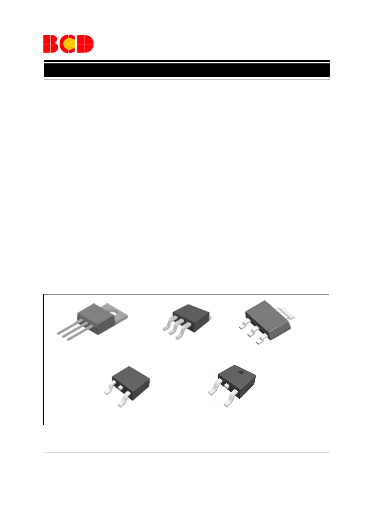
The AZ2940 series is available in the industry standard
TO-220-3, TO-263-3, TO-252-2 (1), TO-252-2 (3) and
SOT-223 power packages. (Detailed information
please refer to page 4)
Features
· Minimum Guaranteed Output Current: 1A
· Dropout Voltage at I
(Except 1.2V and 1.8V Versions)
· Output Accuracy:
· Low Ground Current
· Internal Current Limit and Thermal Protection
· Reversed-battery and Reversed-lead Insertion
Protection
· Fast Transient Response
± 1%
=1A: 280mV Typ.
OUT
Applications
· LCD TV
· Set Top Box
· LCD Monitor
· SMPS Post Regulator
· Laptop, Palmtop and Notebook
· Portable Instrumentation
· USB Power Supply
TO-220-3 TO-263-3
TO-252-2 (1)
Figure 1. Package Types of AZ2940
Sept. 2011 Rev. 2. 4 BCD Semiconductor Manufacturing Limited
1
TO-252-2 (3)
SOT-223
Page 2
Data Sheet
1A ULTRA LOW DROPOUT LINEAR REGULATOR AZ2940
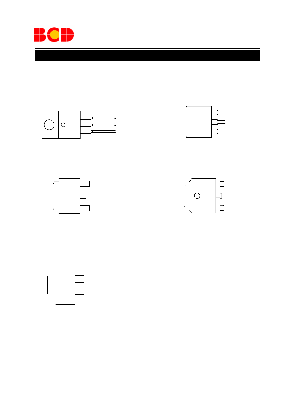
Pin Configuration
T Package
(TO-220-3)
3
2
1
(TO-252-2 (1))
3
2
1
V
OUT
GND
V
IN
V
OUT
GND
V
IN
D Package
S Package
(TO-263-3)
3
2
1
(TO-252-2 (3))
3
2
1
V
OUT
GND
V
IN
V
OUT
GND
V
IN
H Package
(SOT-223)
3
2
1
V
GND
V
OUT
IN
Figure 2. Pin Configuration of AZ2940 (Top View)
Sept. 2011 Rev. 2. 4 BCD Semiconductor Manufacturing Limited
2
Page 3
Data Sheet
1A ULTRA LOW DROPOUT LINEAR REGULATOR AZ2940
Pin Description
Pin Number Pin Name Function
1V
2 GND Ground pin. This pin and TAB are internally connected
3V
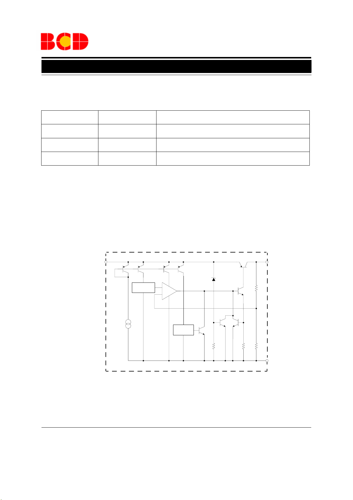
Functional Block Diagram
1
V
IN
IN
OUT
Reference +
Unregulated Input
Regulated Output
1.24V
-
16V
3
V
OUT
Thermal
Shutdown
2
GND
Figure 3. Functional Block Diagram of AZ2940
Sept. 2011 Rev. 2. 4 BCD Semiconductor Manufacturing Limited
3
Page 4
Data Sheet
1A ULTRA LOW DROPOUT LINEAR REGULATOR AZ2940
Ordering Information
-
AZ2940
Package
TO-220-3
TO-263-3
TO-252-2 (1)
/TO-252-2 (3)
SOT-223
Circuit Type
Package
T: TO-220-3
S: TO-263-3
D: TO-252-2 (1)/TO-252-2 (3)
H: SOT-223
Temperature
Range
-40 to 125
-40 to 125oC
-40 to 125
-40 to 125
o
C
o
C
o
C
Lead Free Green Lead Free Green
AZ2940T-3.3E1 AZ2940T-3.3G1 AZ2940T-3.3E1 AZ2940T-3.3G1 Tube
AZ2940T-5.0E1 AZ2940T-5.0G1 AZ2940T-5.0E1 AZ2940T-5.0G1 Tube
AZ2940S-3.3E1 AZ2940S-3.3G1 AZ2940S-3.3E1 AZ2940S-3.3G1 Tube
AZ2940S-3.3TRE1 AZ2940S-3.3TRG1 AZ2940S-3.3E1 AZ2940S-3.3G1 Tape & Reel
AZ2940S-5.0E1 AZ2940S-5.0G1 AZ2940S-5.0E1 AZ2940S-5.0G1 Tube
AZ2940S-5.0TRE1 AZ2940S-5.0TRG1 AZ2940S-5.0E1 AZ2940S-5.0G1 Tape & Reel
AZ2940D-1.8E1 AZ2940D-1.8G1 AZ2940D-1.8E1 AZ2940D-1.8G1 Tube
AZ2940D-1.8TRE1 AZ2940D-1.8TRG1 AZ2940D-1.8E1 AZ2940D-1.8G1 Tape & Reel
AZ2940D-2.5E1 AZ2940D-2.5G1 AZ2940D-2.5E1 AZ2940D-2.5G1 Tube
AZ2940D-2.5TRE1 AZ2940D-2.5TRG1 AZ2940D-2.5E1 AZ2940D-2.5G1 Tape & Reel
AZ2940D-3.3E1 AZ2940D-3.3G1 AZ2940D-3.3E1 AZ2940D-3.3G1 Tube
AZ2940D-3.3TRE1 AZ2940D-3.3TRG1 AZ2940D-3.3E1 AZ2940D-3.3G1 Tape & Reel
AZ2940D-5.0E1 AZ2940D-5.0G1 AZ2940D-5.0E1 AZ2940D-5.0G1 Tube
AZ2940D-5.0TRE1 AZ2940D-5.0TRG1 AZ2940D-5.0E1 AZ2940D-5.0G1 Tape & Reel
E1: Lead Free
G1: Green
TR: Tape and Reel
Blank: Tube
1.2: Fixed Output 1.2V
1.8: Fixed Output 1.8V
2.5: Fixed Output 2.5V
3.3: Fixed Output 3.3V
5.0: Fixed Output 5.0V
Part Number Marking ID
AZ2940D-1.2G1 AZ2940D-1.2G1 Tube
AZ2940D-1.2TRG1 AZ2940D-1.2G1 Tape & Reel
AZ2940H-1.2TRG1 GH12B Tape & Reel
AZ2940H-1.8TRG1 GH12F Tape & Reel
AZ2940H-2.5TRG1 GH12G Tape & Reel
AZ2940H-3.3TRG1 GH12H Tape & Reel
AZ2940H-5.0TRG1 GH12J Tape & Reel
Packing
Typ e
BCD Semiconductor's Pb-free products, as designated with "E1" suffix in the part number, are RoHS compliant. Products with
"G1" suffix are available in green packages.
Sept. 2011 Rev. 2. 4 BCD Semiconductor Manufacturing Limited
4
Page 5
Data Sheet
1A ULTRA LOW DROPOUT LINEAR REGULATOR AZ2940
Absolute Maximum Ratings (Note 1)
Parameter Symbol
Input Voltage V
Operating Junction Temperature T
Storage Temperature Range T
Lead Temperature (Soldering, 10sec) T
IN
J
STG
LEAD
Va lu e
16 V
150
-65 to 150
260
Unit
o
C
o
C
o
C
TO-220-3 60
Thermal Resistance
θ
JA
TO-263-3 60
o
C/W
TO-252-2 (1)/TO-252-2 (3) 100
SOT-223 120
ESD (Human Body Model) ESD 5000 V
ESD (Machine Model) ESD 300 V
Note 1: Stresses greater than those listed under "Absolute Maximum Ratings" may cause permanent damage to
the device. These are stress ratings only, and functional operation of the device at these or any other conditions
beyond those indicated under "Recommended Operating Conditions" is not implied. Exposure to "Absolute Maximum Ratings" for extended periods may affect device reliability.
Recommended Operating Conditions
Parameter Symbol Min Max Unit
Input Voltage
Operating Junction Temperature
VIN
T
2.5 13.2 V
J
-40 125
o
C
Sept. 2011 Rev. 2. 4 BCD Semiconductor Manufacturing Limited
5
Page 6
Data Sheet
1A ULTRA LOW DROPOUT LINEAR REGULATOR AZ2940
Electrical Characteristics
AZ2940-1.2 Electrical Characteristics
Operating Conditions: V
The Boldface applies over -40
Parameter Symbol Condition Min Typ Max Unit
Output Voltage
Line Regulation V
Load Regulation V
Output Voltage
Temperature Coefficient
Ground Current
Short Circuit Current I
Minimum Load Current I
Output Noise Voltage (rms) 10Hz to 100KHz, I
Thermal Resistance
=2.5V, I
IN
o
C≤TJ≤125oC.
V
∆V
I
LOAD (MIN)
OUT
OUT
RLINE
RLOAD
/∆TI
OUT
GND
SC
θ
JC
=10mA, CIN=10µF, C
I
=10mA 1.188 1.2 1.212 V
OUT
10mA≤I
I
OUT
VIN=2.5V, 10mA≤I
OUT
VIN=2.5V
V
OUT
C
OUT
≤1A, 2.5V≤VIN≤13.2V 1.176 1.2 1.224 V
OUT
=10mA, 2.5V≤VIN≤13.2V 3.6 18 mV
=10mA 180
I
OUT
I
OUT
=0V (Note 2) 1.5 2.2 A
=10µF
=10µF, TJ=25oC, unless otherwise specified.
OUT
≤1A 5.4 27 mV
OUT
=750mA 12 25 mA
=1A 18 mA
=100mA,
OUT
TO-252-2 (1)/TO-252-2 (3) 7.8
SOT-223 29.7
µV/
15mA
400 µV
o
C/W
o
C
Note 2: VIN=V
OUT(NOMINAL)
+1V.
Sept. 2011 Rev. 2. 4 BCD Semiconductor Manufacturing Limited
6
Page 7
Data Sheet
1A ULTRA LOW DROPOUT LINEAR REGULATOR AZ2940
Electrical Characteristics
AZ2940-1.8 Electrical Characteristics
Operating Conditions: V
The Boldface applies over -40
Parameter Symbol Condition Min Typ Max Unit
Output Voltage
Line Regulation V
Load Regulation V
Output Voltage
Temperature Coefficient
Dropout Voltage (Note 3)
Ground Current
Short Circuit Current I
Minimum Load Current I
Output Noise Voltage (rms) 10Hz to 100KHz, I
Thermal Resistance
=2.8V, I
IN
o
C≤TJ≤125oC.
V
∆V
V
I
LOAD (MIN)
OUT
OUT
RLINE
RLOAD
/∆TI
OUT
DROP
GND
SC
θ
JC
=10mA, CIN=10µF, C
I
=10mA 1.782 1.8 1.818 V
OUT
10mA≤I
I
OUT
VIN=2.8V, 10mA≤I
OUT
∆V
OUT
VIN=2.8V
V
OUT
C
OUT
≤1A, 2.8V≤VIN≤13.2V 1.764 1.8 1.836 V
OUT
=10mA, 2.8V≤VIN≤13.2V 3.6 18 mV
=10mA 36 180
I
=1%
I
I
I
OUT
OUT
OUT
OUT
=0V (Note 2) 1.5 2.2 A
=10µF
=10µF, TJ=25oC, unless otherwise specified.
OUT
≤1A 5.4 27 mV
OUT
=100mA 290 500 mV
=1A 330 750 mV
=750mA 12 25 mA
=1A 18 mA
=100mA,
OUT
TO-252-2 (1)/TO-252-2 (3) 7.8
SOT-223 29.7
15mA
400 µV
µV/
o
C/W
o
C
Note 2: VIN=V
OUT(NOMINAL)
+1V.
Note 3: Dropout voltage is defined as the input-to-output differential when the output voltage drops to 99% of its nominal value
which is measured at V
+1V applied to VIN. In application, VIN should be no less than 2.5V.
OUT
Sept. 2011 Rev. 2. 4 BCD Semiconductor Manufacturing Limited
7
Page 8

Data Sheet
1A ULTRA LOW DROPOUT LINEAR REGULATOR AZ2940
Electrical Characteristics (Continued)
AZ2940-2.5 Electrical Characteristics
Operating Conditions: V
The Boldface applies over -40
Parameter Symbol Condition Min Typ Max Unit
Output Voltage
Line Regulation V
Load Regulation V
Output Voltage
Temperature Coefficient
Dropout Voltage (Note 4)
Ground Current
Short Circuit Current I
Minimum Load Current I
Output Noise Voltage (rms) 10Hz to 100KHz, I
Thermal Resistance
=3.5V, I
IN
o
C≤TJ≤125oC.
V
∆V
V
I
LOAD (MIN)
OUT
OUT
RLINE
RLOAD
/∆TI
OUT
DROP
GND
SC
θ
JC
=10mA, CIN=10µF, C
I
=10mA 2.475 2.5 2.525 V
OUT
10mA≤I
I
OUT
VIN=3.5V, 10mA≤I
OUT
∆V
OUT
VIN=3.5V
V
OUT
C
OUT
≤1A, 3.5V≤VIN≤13.2V 2.45 2.5 2.55 V
OUT
=10mA, 3.5V≤VIN≤13.2V 5.0 25 mV
=10mA 50 250
I
=1%
I
I
I
OUT
OUT
OUT
OUT
=0V (Note 2) 1.5 2.2 A
=10µF
=10µF, TJ=25oC, unless otherwise specified.
OUT
≤1A 7.5 37.5 mV
OUT
=100mA 70 200 mV
=1A 280 550 mV
=750mA 12 25 mA
=1A 18 mA
=100mA,
OUT
TO-252-2 (1)/TO-252-2 (3) 7.8
SOT-223 29.7
15mA
400 µV
µV/
o
C/W
o
C
Note 2: VIN=V
OUT(NOMINAL)
+1V.
Note 4: Dropout voltage is defined as the input-to-output differential when the output voltage drops to 99% of its nominal value
which is measured at V
+1V applied to VIN.
OUT
Sept. 2011 Rev. 2. 4 BCD Semiconductor Manufacturing Limited
8
Page 9

Data Sheet
1A ULTRA LOW DROPOUT LINEAR REGULATOR AZ2940
Electrical Characteristics (Continued)
AZ2940-3.3 Electrical Characteristics
Operating Conditions: V
The Boldface applies over -40
Parameter Symbol Condition Min Typ Max Unit
Output Voltage
Line Regulation V
Load Regulation V
Output Voltage
Temperature Coefficient
Dropout Voltage (Note 4)
Ground Current
Short Circuit Current I
Minimum Load Current I
Output Noise Voltage (rms) 10Hz to 100KHz, I
Thermal Resistance
=4.3V, I
IN
o
C≤TJ≤125oC.
V
∆V
V
I
LOAD (MIN)
OUT
OUT
RLINE
RLOAD
/∆TI
OUT
DROP
GND
SC
θ
JC
=10mA, CIN=10µF, C
I
=10mA 3.27 3.3 3.33 V
OUT
10mA≤I
I
OUT
VIN=4.3V, 10mA≤I
OUT
∆V
OUT
VIN=4.3V
V
OUT
C
OUT
≤1A, 4.3V≤VIN≤13.2V 3.23 3.3 3.37 V
OUT
=10mA, 4.3V≤VIN≤13.2V 6.6 33 mV
=10mA 66 330
I
=1%
I
I
I
OUT
OUT
OUT
OUT
=0V (Note 2) 1.5 2.2 A
=10µF
=10µF, TJ=25oC, unless otherwise specified.
OUT
≤1A 9.9 50 mV
OUT
=100mA 70 200 mV
=1A 280 550 mV
=750mA 12 25 mA
=1A 18 mA
=100mA,
OUT
TO-220-3 4.4
TO-263-3 4.4
TO-252-2 (1)/TO-252-2 (3) 7.8
SOT-223 29.7
15mA
400 µV
µV/
o
C/W
o
C
Note 2: VIN=V
OUT(NOMINAL)
+1V.
Note 4: Dropout voltage is defined as the input-to-output differential when the output voltage drops to 99% of its nominal
value which is measured at V
+1V applied to VIN.
OUT
Sept. 2011 Rev. 2. 4 BCD Semiconductor Manufacturing Limited
9
Page 10

Data Sheet
1A ULTRA LOW DROPOUT LINEAR REGULATOR AZ2940
Electrical Characteristics (Continued)
AZ2940-5.0 Electrical Characteristics
Operating Conditions: VIN=6V, I
Boldface applies over -40
o
C≤TJ≤125oC.
=10mA, CIN=10µF, C
OUT
=10µF, TJ=25oC, unless otherwise specified. The
OUT
Parameter Symbol Condition Min Typ Max Unit
Output Voltage
Line Regulation V
Load Regulation V
Output Voltage
V
∆V
OUT
RLINE
RLOAD
/∆T I
OUT
I
=10mA 4.95 5.0 5.05 V
OUT
10mA≤I
I
OUT
VIN=6V, 10mA≤I
OUT
≤1A, 6V≤VIN≤13.2V 4.90 5.0 5.10 V
OUT
=10mA, 6V≤VIN≤13.2V 10 50 mV
≤1A 15 75 mV
OUT
=10mA 100 500
µV/
Temperature Coefficient
=1%
I
=100mA 70 200 mV
OUT
I
=1A 280 550 mV
OUT
=750mA 12 25 mA
I
OUT
I
=1A 18 mA
OUT
15 mA
OUT
=100mA,
400 µV
o
C/W
Dropout Voltage (Note 4)
V
DROP
∆V
OUT
Ground Current
Short Circuit Current I
Minimum Load Current I
I
GND
SC
LOAD (MIN)
VIN=6V
V
=0V (Note 3) 1.5 2.2 A
OUT
Output Noise Voltage (rms) 10Hz to 100KHz, I
=10µF
C
OUT
TO-220-3 4.4
Thermal Resistance
θ
JC
TO-263-3 4.4
TO-252-2 (1)/TO-252-2 (3) 7.8
SOT-223 29.7
o
C
Note 2: VIN=V
OUT(NOMINAL)
+1V.
Note 4: Dropout voltage is defined as the input-to-output differential when the output voltage drops to 99% of its nominal
value which is measured at V
+1V applied to VIN.
OUT
Sept. 2011 Rev. 2. 4 BCD Semiconductor Manufacturing Limited
10
Page 11

Data Sheet
1A ULTRA LOW DROPOUT LINEAR REGULATOR AZ2940
Typical Performance Characteristics
5.020
5.018
5.016
5.014
5.012
5.010
5.008
5.006
Output Voltage (V)
5.004
5.002
5.000
6 7 8 9 10 11 12 13 14
AZ2940-5.0
Input Voltage (V)
Figure 4. Line Regulation
25.0
22.5
20.0
17.5
15.0
12.5
10.0
7.5
Ground Current (mA)
5.0
2.5
0.0
0 250 500 750 1000
AZ2940-5.0
VIN=6V
TJ=25oC
Output Current (mA)
I
=10mA
OUT
TJ=25oC
5.0250
5.0225
5.0200
5.0175
5.0150
5.0125
5.0100
Output Voltage (V)
5.0075
5.0050
5.0025
5.0000
0 250 500 750 1000
AZ2940-5.0
VIN=6V
TJ=25oC
Output Current (mA)
Figure 5. Load Regulation
20
18
16
14
12
10
8
6
Ground Current (mA)
4
2
0
0246810121416
I
I
Input Voltage (V)
=100mA
OUT
=1A
OUT
TJ=25oC
Figure 6. Ground Current vs. Output Current
Figure 7. Ground Current vs. Input Voltage
Sept. 2011 Rev. 2. 4 BCD Semiconductor Manufacturing Limited
11
Page 12

Data Sheet
1A ULTRA LOW DROPOUT LINEAR REGULATOR AZ2940
Typical Performance Characteristics (Continued)
500
450
400
350
300
250
200
150
Dropout Voltage (mV)
100
50
0
0 250 500 750 1000
AZ2940-5.0
Output Current (mA)
Figure 8. Dropout Voltage vs. Output Current
3.50
3.25
3.00
2.75
2.50
2.25
Ground Current (mA)
2.00
1.75
1.50
-25 0 25 50 75 100 125
Junction Temperature (oC)
AZ2940-5.0
VIN=6V
I
=500mA
OUT
TJ=25oC
0.37
0.36
0.35
0.34
0.33
0.32
0.31
0.30
Ground Current (mA)
0.29
0.28
0.27
-25 0 25 50 75 100 125
AZ2940-5.0
VIN=6V
I
=10mA
OUT
Junction Temperature (oC)
Figure 9. Ground Current vs. Junction Temperature
10.0
9.5
9.0
8.5
8.0
Ground Current (mA)
7.5
7.0
6.5
6.0
5.5
5.0
-25 0 25 50 75 100 125
Junction Temperature (oC)
AZ2940-5.0
VIN=6V
I
=1A
OUT
Figure 10. Ground Current vs. Junction Temperature
Figure 11. Ground Current vs. Junction Temperature
Sept. 2011 Rev. 2. 4 BCD Semiconductor Manufacturing Limited
12
Page 13

Data Sheet
1A ULTRA LOW DROPOUT LINEAR REGULATOR AZ2940
Typical Performance Characteristics (Continued)
500
475
450
425
400
375
350
325
300
Dropout Voltage (mV)
275
250
225
200
-25 0 25 50 75 100 125
AZ2940-5.0
I
OUT
=750mA
Junction Temperature (oC)
Figure 12. Dropout Voltage vs. Junction Temperature
5.05
5.04
5.03
5.02
5.01
5.00
4.99
Output Voltage (V)
4.98
4.97
4.96
4.95
-25 0 25 50 75 100 125
AZ2940-5.0
Junction Temperature (oC)
VIN=6V
I
=10mA
OUT
500
475
450
425
400
375
350
325
300
Dropout Voltage (mV)
275
250
225
200
AZ2940-5.0
I
=1A
OUT
-25 0 25 50 75 100 125
Junction Temperature (oC)
Figure 13. Dropout Voltage vs. Junction Temperature
100
C
=2.2µF
OUT
=5V
V
10
1
Output Capacitor ESR (Ω)
0.1
Stable Range
Unstable Range
0.01
0 20406080100
Output Current (mA)
T
OUT
=25OC
A
Figure 14. Output Voltage vs. Junction Temperature
Figure 15. Output Capacitor ESR vs. Output Current
Sept. 2011 Rev. 2. 4 BCD Semiconductor Manufacturing Limited
13
Page 14

Data Sheet
1A ULTRA LOW DROPOUT LINEAR REGULATOR AZ2940
Typical Performance Characteristics (Continued)
100
C
=10µF
OUT
=5V
V
10
1
0.1
Output Capacitor ESR (Ω)
0.01
0 200 400 600 800 1000
Stable Range
Unstable Range
Output Current (mA)
OUT
T
A
=25OC
Figure 16. Output Capacitor ESR vs. Output Current
0.4
0.2
0
(0.2V/Div)
OUT
-0.2
AZ2940-5.0
C
=47µF
OUT
∆V
(0.2V/Div)
OUT
∆V
(0.5A/Div)
I
(0.02V/Div)
OUT
∆V
OUT
0.06
0.04
0.02
0.4
0.2
-0.2
0.5
-0.5
AZ2940-5.0
C
=10µF
OUT
0
1
0
Time (200µs/Div)
Figure 17. Load Transient
AZ2940-5.0
I
=10mA
OUT
0
(0.5A/Div)
OUT
I
1
0.5
0
-0.5
Time (200µs/Div)
Figure 18. Load Transient
(0.5V/Div)
IN
∆V
1
0.5
0
-0.5
Time (200µs/Div)
Figure 19. Line Transient
Sept. 2011 Rev. 2. 4 BCD Semiconductor Manufacturing Limited
14
Page 15

Data Sheet
1A ULTRA LOW DROPOUT LINEAR REGULATOR AZ2940
Typical Performance Characteristics (Continued)
50
45
40
35
30
25
20
15
Power Dissipation (W)
10
5
0
-25 0 25 50 75 100 125
Package:TO-220-3
45*43mm2 Heatsink
No Heatsink
Case Temperature (oC)
Figure 20. Power Dissipation vs. Case Temperature
50
45
40
35
30
25
20
15
Power Dissipation (W)
10
5
0
-25 0 25 50 75 100 125
Case Temperature (oC)
Package:TO-263-3
45*43mm2 Heatsink
No Heatsink
50
45
40
35
30
25
20
15
Power Dissipation (W)
10
5
0
-25 0 25 50 75 100 125
Package:TO-252-2 (1)/TO-252-2 (3)
45*43mm2 Heatsink
No Heatsink
Case Temperature (oC)
Figure 21. Power Dissipation vs. Case Temperature
Figure 22. Power Dissipation vs. Case Temperature
Sept. 2011 Rev. 2. 4 BCD Semiconductor Manufacturing Limited
15
Page 16

Data Sheet
1A ULTRA LOW DROPOUT LINEAR REGULATOR AZ2940
Typical Application
Note: C
is required if regulator is located far from power supply filter and is recommended to be 0.47µF or greater. To main-
IN
tain stability, C
1
V
IN
VIN V
OUT
3
V
OUT
AZ2940
+
C
IN
GND
2
Figure 23. Typical Application of AZ2940
is recommended to be 2.2µF or greater. The ESR of this capacitor is critical, please see curve.
OUT
+
C
OUT
Sept. 2011 Rev. 2. 4 BCD Semiconductor Manufacturing Limited
16
Page 17

Data Sheet
1A ULTRA LOW DROPOUT LINEAR REGULATOR AZ2940
Mechanical Dimensions
TO-220-3 Unit: mm(inch)
φ
1.500(0.059)
1.160(0.046)
1.760(0.069)
60
9.660(0.380)
10.660(0. 420)
°
φ
3.560(0.140)
4.060(0.160)
2
.
8
5
8
3
.
3
)
)
5
5
3
7
3
3
.
.
0
0
(
(
0
0
2
2
5
5
.
.
8
9
0.381(0.015)
0
2
)
(
0
0
.
1
0
(
0
3
)
3
.
1
)
3
7
0
.
0
(
0
5
8
.
1
)
)
0
0
5
6
6
5
.
.
0
0
(
(
0
0
1
3
5
2
.
.
6
4
1
)
)
8
2
9
9
0
1
.
.
1
1
(
(
0
0
8
8
8
2
.
.
7
0
2
3
1
3
°
0.550(0.022)
1.350(0.053)
0.200(0.008)
3.560(0.140)
4.820(0.190)
7
°
2.080(0.082)
2.880(0.113)
7
°
0.813(0.032)
6
0
°
2.540(0.100)
3
8
6
(
0
.
7
0.381(0.015)
2.540(0.100)
4
.
3
5
)
0.356 (0.014)
0.610(0.024)
Sept. 2011 Rev. 2. 4 BCD Semiconductor Manufacturing Limited
17
Page 18

Data Sheet
1A ULTRA LOW DROPOUT LINEAR REGULATOR AZ2940
Mechanical Dimensions (Continued)
TO-263-3 Unit: mm(inch)
1
.
0
(
0
7
0
.
4
0
2
8
.
4
7
0
°
)
)
0
0
8
4
3
3
.
.
0
0
(
(
0
0
5
4
6
6
.
.
9
8
2.540(0.100)
)
0
6
)
0
9
1
.
0
(
9.650(0.380)
10.290(0.405)
8.840(0.348)
3°
1.270(0.050)
1.390(0.055)
1
4
5
1
1.150(0.045)
1.390(0.055)
0.510(0.020)
0.990(0.039)
2.540(0.100)
1.150(0.045)
1.390(0.055)
7°
0.020(0.001)
0.250(0.010)
2.640(0.104)
)
1
8
5
.
0
(
0
6
7
.
2
6
.
0
(
0
4
7
.
)
0
)
)
4
6
9
0
0
1
.
.
0
0
(
(
0
9
3
.
2
3°
0
9
6
.
2
0.380(0.015)
0°
6°
2.700(0.106)
0.360(0.014)
0.400(0.016)
7°
0
.
0
(
0
0
2
.
2
2
°
8
°
2.540(0.100)
7
8
)
7.420(0.292)
)
0
2
2
.
0
(
0
0
6
.
5
7.980(0.314)
2.540(0.100)
Sept. 2011 Rev. 2. 4 BCD Semiconductor Manufacturing Limited
18
Page 19

Data Sheet
1A ULTRA LOW DROPOUT LINEAR REGULATOR AZ2940
Mechanical Dimensions (Continued)
SOT-223 Unit: mm(inch)
6.300(0.248)
6.700(0.264)
6.700(0.264)
.
2.900(0.114)
3.100(0.122)
0.900(0.035)
MIN
0.250(0.010)
7.300(0.287)
3.300(0.130)
3.700(0.146)
0
0
1
0
.
0
(
0
5
2
0
.
0
(
0
5
.3
)
0
)
4
1
1.750(0.069)
TYP
2.300(0.091)
1.500(0.059)
1.700(0.067)
TYP
0.020(0.001)
0.100(0.004)
4.500(0.177)
4.700(0.185)
0.610(0.024)
0.810(0.032)
1.520(0.060)
1.800(0.071)
0°
10°
Sept. 2011 Rev. 2. 4 BCD Semiconductor Manufacturing Limited
19
Page 20

Data Sheet
1A ULTRA LOW DROPOUT LINEAR REGULATOR AZ2940
Mechanical Dimensions (Continued)
TO-252-2 (1) Unit: mm(inch)
6.450(0.254)
6.650(0.262)
5.200(0.205)
1.650(0.065)
0.900(0.035)
5.400(0.213)
1.350(0.053)
9.500(0.374)
0.600(0.024)
9.900(0.390)
0.450(0.018)
0.580(0.023)
0.000(0.000)
0.127(0.005)
5°
2.200(0.087)
2.400(0.094)
8
°
5°
5.450(0.215)
4.300(0.169)
5.400(0.213)
6.250(0.246)
4.800(0.189)
6.500(0.256)
2.300TYP
4.500(0.177)
4.700(0.185)
0.700(0.028)
0.900(0.035)
0.500(0.020)
0.700(0.028)
3°
4°
0.450(0.018)
0.580(0.023)
2.550(0.100)
1.400(0.055)
1.780(0.070)
2.900(0.114)
3.800REF(0.150REF)
Sept. 2011 Rev. 2. 4 BCD Semiconductor Manufacturing Limited
20
Page 21

Data Sheet
1A ULTRA LOW DROPOUT LINEAR REGULATOR AZ2940
Mechanical Dimensions (Continued)
TO-252-2 (3) Unit: mm(inch)
6.500(0.256)
6.700(0.264)
0.900(0.035)
1.250(0.049)
6.000(0.236)
6.200(0.244)
1.800REF
0.720(0.028)
0.900(0.035)
2.286(0.090)
BSC
5.130(0.202)
5.460(0.215)
5
9
1.29±0.1
0.150(0.006)
0.750(0.030)
0.720(0.028)
0.850(0.033)
2.200(0.087)
2.380(0.094)
4.700REF
0.470(0.019)
0.600(0.024)
5
9
0
8
0.900(0.035)
1.100(0.043)
3
7
5.250REF
0
0.600(0.024)
1.000(0.039)
8
9.800(0.386)
10.40(0.409)
2.900REF
1.400(0.055)
1.700(0.067)
Sept. 2011 Rev. 2. 4 BCD Semiconductor Manufacturing Limited
21
Page 22

BCD Semiconductor Manufacturing Limited
IMPORTANT NOTICE
IMPORTANT NOTICE
BCD Semiconductor Manufacturing Limited reserves the right to make changes without further notice to any products or specifi-
BCD Semiconductor Manufacturing Limited reserves the right to make changes without further notice to any products or specifi-
cations herein. BCD Semiconductor Manufacturing Limited does not assume any responsibility for use of any its products for any
cations herein. BCD Semiconductor Manufacturing Limited does not assume any responsibility for use of any its products for any
particular purpose, nor does BCD Semiconductor Manufacturing Limited assume any liability arising out of the application or use
particular purpose, nor does BCD Semiconductor Manufacturing Limited assume any liability arising out of the application or use
of any its products or circuits. BCD Semiconductor Manufacturing Limited does not convey any license under its patent rights or
of any its products or circuits. BCD Semiconductor Manufacturing Limited does not convey any license under its patent rights or
other rights nor the rights of others.
other rights nor the rights of others.
http://www.bcdsemi.com
MAIN SITE
MAIN SITE
- Headquarters
BCD Semiconductor Manufacturing Limited
BCD Semiconductor Manufactur ing Limited
- Wafer Fab
No. 1600, Zi Xing Road, Shanghai ZiZhu Science-based Industrial Park, 200241, China
Shanghai SIM-BCD Semiconductor Manufacturing Limited
Tel: +86-21-24162266, Fax: +86-21-24162277
800, Yi Shan Road, Shanghai 200233, China
Tel: +86-21-6485 1491, Fax: +86-21-5450 0008
REGIONAL SALES OFFICE
Shenzhen Office
REGIONAL SALES OFFICE
Shanghai SIM-BCD Semiconductor Manufacturing Co., Ltd., Shenzhen Office
Shenzhen Office
Unit A Room 1203, Skyworth Bldg., Gaoxin Ave.1.S., Nanshan District, Shenzhen,
Shanghai SIM-BCD Semiconductor Manufacturing Co., Ltd. Shenzhen Office
China
Advanced Analog Circuits (Shanghai) Corporation Shenzhen Office
Tel: +86-755-8826 7951
Room E, 5F, Noble Center, No.1006, 3rd Fuzhong Road, Futian District, Shenzhen 518026, China
Fax: +86-755-8826 7865
Tel: +86-755-8826 7951
Fax: +86-755-8826 7865
- Wafer Fab
BCD Semiconductor Manufacturing Limited
Shanghai SIM-BCD Semiconductor Manufacturing Co., Ltd.
- IC Design Group
800 Yi Shan Road, Shanghai 200233, China
Advanced Analog Circuits (Shanghai) Corporation
Tel: +86-21-6485 1491, Fax: +86-21-5450 0008
8F, Zone B, 900, Yi Shan Road, Shanghai 200233, China
Tel: +86-21-6495 9539, Fax: +86-21-6485 9673
Taiwan Office
BCD Semiconductor (Taiwan) Company Limited
Taiwan Office
4F, 298-1, Rui Guang Road, Nei-Hu District, Taipei,
BCD Semiconductor (Taiwan) Company Limited
Tai wan
4F, 298-1, Rui Guang Road, Nei-Hu District, Taipei,
Tel: +886-2-2656 2808
Taiwan
Fax: +886-2-2656 2806
Tel: +886-2-2656 2808
Fax: +886-2-2656 2806
USA Office
BCD Semiconductor Corp.
USA Office
30920 Huntwood Ave. Hayward,
BCD Semiconductor Corporation
CA 94544, USA
30920 Huntwood Ave. Hayward,
Tel : +1-510-324-2988
CA 94544, U.S.A
Fax: +1-510-324-2788
Tel : +1-510-324-2988
Fax: +1-510-324-2788
 Loading...