

Page 1
AZ2085
Document number: DS36595 Rev. 3 - 2
1 of 11
www.diodes.com
March 2014
© Diodes Incorporated
AZ2085
A Product Line of
Diodes Incorporated
NE W P R OD U C T
Description
The AZ2085 series is low dropout positive voltage regulators with a
maximum dropout of 1.5V at 3A of load current.
The device features on-chip thermal shutdown. It also includes a
bandgap reference and a current limiting circuit.
The AZ2085 is available in adjustable version. The adjustable version
can set the output voltage with two external resistors.
The AZ2085 series is available in standard packages of TO252-2 (3)
and TO252-2 (5).
Applications
High Efficiency Linear Regulators
Battery Charger
Digital Video/Camcorder
Post Regulation for Switching Supplies
Microprocessor Supply
Mother Board Power Supplies
DVD-video Player
Telecom Equipment
Set Top Boxes and Web Boxes Modules' Supply
Features
Low Dropout Voltage: Typical 1.2V at 3A
Current Limiting and Thermal Protection
Output Current: 3A
Current Limit: 4.5A
Operating Junction Temperature: 0 to +125°C
Line Regulation: 0.015% (Typ)
Load Regulation: 0.1% (Typ)
Adjust Pin Current: 6μA (Typ)
Minimum Load Current: 0.3mA (Typ)
Compatible with Low ESR Ceramic Capacitor
Totally Lead-Free & Fully RoHS Compliant (Notes 1 & 2)
Halogen and Antimony Free. “Green” Device (Note 3)
1
2
3
INPUT
OUTPUT
ADJ/GND
1
2
3
INPUT
OUTPUT
ADJ/GND
1
2
3
INPUT
OUTPUT
ADJ/GND
3A LOW DROPOUT LINEAR REGULATOR
Notes: 1. No purposely added lead. Fully EU Directive 2002/95/EC (RoHS) & 2011/65/EU (RoHS 2) compliant.
2. See http://www.diodes.com/quality/lead_free.html for more information about Diodes Incorporated’s definitions of Halogen - and Antimony-free, "Green"
and Lead-free.
3. Halogen- and Antimony-free "Green” products are defined as those which contain <900ppm bromine, <900ppm chlorine (<1500ppm total Br + Cl) and
<1000ppm antimony compounds.
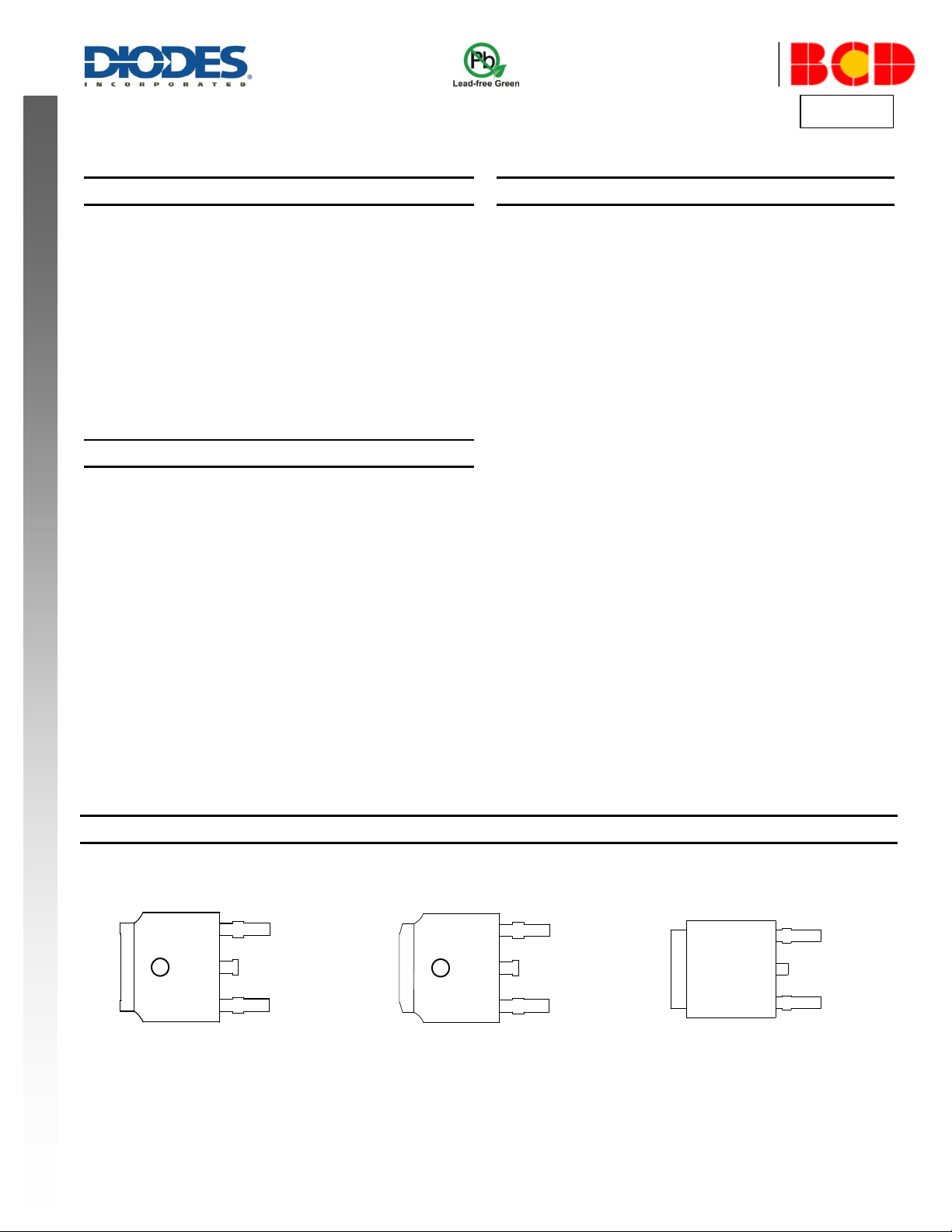
Pin Assignments
(Top View) (Top View) (Top View)
TO252-2 (3) Option 1 TO252-2 (3) Option 2 TO252-2 (5)
Page 2
AZ2085
Document number: DS36595 Rev. 3 - 2
2 of 11
www.diodes.com
March 2014
© Diodes Incorporated
AZ2085
A Product Line of
Diodes Incorporated
NE W P R OD U C T
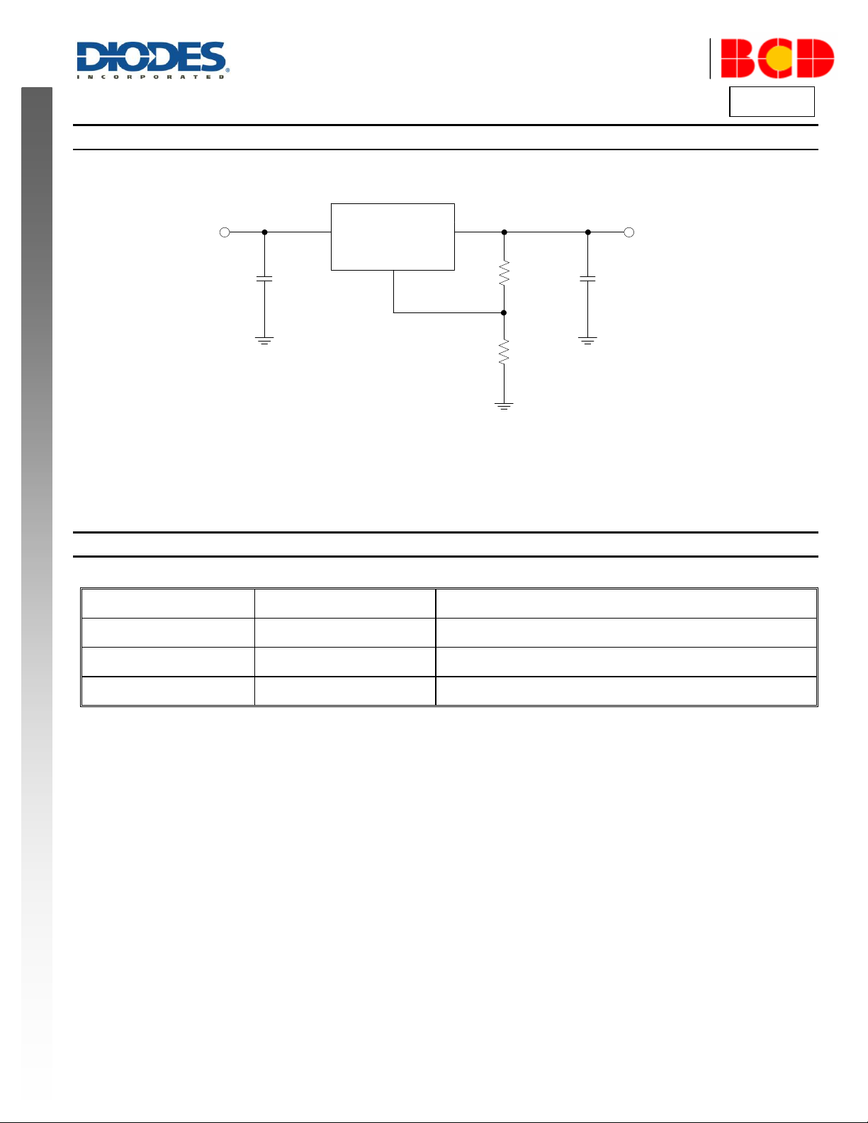
AZ2085
ADJ/GND
V
OUT
= V
REF
* (1+R2/R1) + I
ADJ
* R2
R2
R1
V
IN
V
OUT
CIN=10µF C
OUT
=22µF
INPUT OUTPUT
3
2
1
Pin Number
Pin Name
Function
1
ADJ/GND
Adjust pin/Ground
2
OUTPUT
Output voltage
3
INPUT
Input voltage
Typical Applications Circuit
Pin Descriptions
Page 3
AZ2085
Document number: DS36595 Rev. 3 - 2
3 of 11
www.diodes.com
March 2014
© Diodes Incorporated
AZ2085
A Product Line of
Diodes Incorporated
NE W P R OD U C T
Thermal
Protection
+
-
For Adjustable Output, disconnect A1 and A2, connect B
INPUT
OUTPUT
ADJ/
GND
A1
A2
B
3
2
1
Functional Block Diagram
Page 4
AZ2085
Document number: DS36595 Rev. 3 - 2
4 of 11
www.diodes.com
March 2014
© Diodes Incorporated
AZ2085
A Product Line of
Diodes Incorporated
NE W P R OD U C T
Symbol
Parameter
Rating
Unit
V
IN
Input Voltage
18
V
T
J
Operating Junction Temperature
+150
°C
T
STG
Storage Temperature Range
-65 to +150
°C
T
LEAD
Lead Temperature (Soldering, 10sec)
+260
°C
θ
JA
Thermal Resistance (Junction to Ambient)
100
°C/W
—
ESD (Human Body Model)
2000
V
Symbol
Parameter
Min
Max
Unit
V
IN
Input Voltage — 12 V T
J
Operating Junction Temperature
0
+125
°C
Absolute Maximum Ratings (Note 4)
Note 4: Stresses greater than those listed under “Absolute Maximum Ratings” may cause permanent damage to the device. These are str ess ratings only, and
functional operation of the device at these or any other conditions beyond those indicated under “Recommended Operating Condi tions” is not implied.
Exposure to “Absolute Maximum Ratings” for extended periods may affect device reliability.
Recommended Operating Conditions
Page 5

AZ2085
Document number: DS36595 Rev. 3 - 2
5 of 11
www.diodes.com
March 2014
© Diodes Incorporated
AZ2085
A Product Line of
Diodes Incorporated
NE W P R OD U C T
Symbol
Parameter
Conditions
Min
Typ
Max
Unit
V
REF
Reference Voltage
I
OUT
= 10mA, VIN-V
OUT
= 3V, TJ = +25°C,
10mA ≤ I
OUT
≤ 3A,
1.5V ≤ VIN-V
OUT
≤ 5V
1.238
1.225
1.250
1.250
1.262
1.275
V
ΔV
OUT/VOUT
Load Regulation
0A ≤ I
OUT
≤ 3A, VIN-V
OUT
= 3V
—
0.1
0.2
0.3
0.4
%
ΔV
OUT
/ΔVIN
Line Regulation
I
OUT
= 10mA,
2.85V ≤ V
IN
≤ 10V
—
0.015
0.035
0.2
0.2
%
V
DROP
Dropout Voltage
I
OUT
= 3A,
ΔV
REF
, ΔV
OUT
= 1%
—
1.2
1.5
V
I
LIMIT
Current Limit
VIN-V
OUT
= 3V
3.2
4.5 — A
I
LOAD
Minimum Load Current
V
IN
= 10V
—
0.3 1 mA
I
ADJ
Adjust Pin Current
V
IN
= 4.25V, I
OUT
= 10mA
— 6 10
μA
ΔI
ADJ
Adjust Pin Current Change
10mA ≤ I
OUT
≤ 3A, 1.5V ≤ VIN-V
OUT
≤ 6V
—
0.3 2 μA
PSRR
Ripple Rejection
f
RIPPLE
= 120Hz, C
OUT
= 22μF, I
OUT
= 3A,
VIN-V
OUT
= 3V
—
72 — dB
—
Long Term Stability
TA = +125°C, 1000Hrs
—
0.5 — %
—
Temperature Stability
I
OUT
= 10mA, VIN-V
OUT
= 1.5V
—
0.5 — %
—
RMS Noise (% of V
OUT
)
TA = +125°C, 10Hz ≤ f ≤ 10kHz
—
0.003 — %
—
OTSD — +130
+150
+170
°C
—
OTSD Hysteresis
— — +20
—
°C
—
Pulse Current
Pulse Width ≤ 100μS
— 7 12
A
θ
JC
Thermal Resistance
(Junction to Case)
— — 7.36 — °C/W
Electrical Characteristics (Typicals and limits appearing in normal type apply for T
apply over the entire operating junction temperature range 0 to +125ºC .)
= +25ºC . Limits appearing in Boldface type
J
Page 6

AZ2085
Document number: DS36595 Rev. 3 - 2
6 of 11
www.diodes.com
March 2014
© Diodes Incorporated
AZ2085
A Product Line of
Diodes Incorporated
NE W P R OD U C T
AZ2085 X - XX XX XX
Packing
Package
TR : Tape & Reel
Product Name
D : TO252-2 (3)/
TO252-2 (5)
Output Voltage
ADJ : Adjustable
G1 : Green
RoHS/Green
Package
Temperature
Range
Part Number
Marking ID
Packing
TO252-2 (3)/
TO252-2 (5)
0 to +125C
AZ2085D-ADJTRG1
AZ2085D-ADJG1
2500/Tape & Reel
XXXXXXD
-ADJG1
YWWAXX
First and Second Lines: Logo and Marking ID
(See Ordering Information)
Third Line: Date Code
Y: Year
WW: Work Week of Molding
A: Assembly House Code
XX: 7th and 8th Digits of Batch No.
Ordering Information
Diodes IC’s Pb-free products with "G1" suffix in the part number, are RoHS compliant and green.
Marking Information
(1) TO252-2 Series
(Top View)
Page 7

AZ2085
Document number: DS36595 Rev. 3 - 2
7 of 11
www.diodes.com
March 2014
© Diodes Incorporated
AZ2085
A Product Line of
Diodes Incorporated
NE W P R OD U C T
1.29±0.1
2.900REF
1
.400(0.05
5
)
1
.700(0.06
7
)
0.470(0.019)
0.600(0.024)
5
9
0
8
9.800(0.386)
10.400(0.409)
2.200(0.087)
2.380(0.094)
0.900(0.035)
1.100(0.043)
4.700REF
6.500(0.256)
6.700(0.264)
5.130(0.202)
5.460(0.215)
0.150(0.006)
0.750(0.030)
6.000(0.236)
6.200(0.244)
0.720(0.028)
0.850(0.033)
2.286(0.090)
BSC
0.720(0.028)
0.900(0.035)
0.900(0.035)
1.250(0.049)
1.800REF
8
0
0.600(0.
0
24)
1.000(0.039)
7
3
9
5
5.250REF
Option 1
Option 2
Package Outline Dimensions (All dimensions in mm(inch).)
(1) Type Package: TO252-2 (3)
Page 8

AZ2085
Document number: DS36595 Rev. 3 - 2
8 of 11
www.diodes.com
March 2014
© Diodes Incorporated
AZ2085
A Product Line of
Diodes Incorporated
NE W P R OD U C T
2.190(0.086)
2.390(0.094)
0.508(0.020)
0°
10°
1.400(0.055)
1.780(0.070)
2.740(0.108)REF
9.400(0.370)
10.400(0.409)
0.000(0.000)
0.130(0.005)
6°
8°
0.450(0.018)
0.580(0.023)
6.000(0.236)
6.200(0.244)
5.210(0.205)
MIN
4.320(0.170)
MIN
6.450(0.254)
6.700(0.264)
5.210(0.205)
5.500(0.217)
0.880(0.035)
1.270(0.050)
0.640(0.025)
1.020(0.040)
0.760(0.030)
1.140(0.045)
2.286(0.090)
0.640(0.025)
0.880(0.035)
Package Outline Dimensions (Cont. All dimensions in mm(inch).)
(2) Package Type: TO252-2 (5)
Page 9

AZ2085
Document number: DS36595 Rev. 3 - 2
9 of 11
www.diodes.com
March 2014
© Diodes Incorporated
AZ2085
A Product Line of
Diodes Incorporated
NE W P R OD U C T
E1X1
Y2
Y1
Z
X2
G
Dimensions
Z
(mm)/(inch)
X1
(mm)/(inch)
X2=Y2
(mm)/(inch)
Y1
(mm)/(inch)
G
(mm)/(inch)
E1
(mm)/(inch)
Value
11.600/0.457
1.500/0.059
7.000/0.276
2.500/0.098
2.100/0.083
2.300/0.091
Suggested Pad Layout
(1) Package Type: TO252-2 (3)
Page 10

AZ2085
Document number: DS36595 Rev. 3 - 2
10 of 11
www.diodes.com
March 2014
© Diodes Incorporated
AZ2085
A Product Line of
Diodes Incorporated
NE W P R OD U C T
E1X1
Y2
Y1
Z
X2
G
Dimensions
Z
(mm)/(inch)
X1
(mm)/(inch)
X2=Y2
(mm)/(inch)
Y1
(mm)/(inch)
G
(mm)/(inch)
E1
(mm)/(inch)
Value
11.600/0.457
1.500/0.059
7.000/0.276
2.500/0.098
2.100/0.083
2.300/0.091
Suggested Pad Layout (Cont.)
(2) Package Type: TO252-2 (5)
Page 11

AZ2085
Document number: DS36595 Rev. 3 - 2
11 of 11
www.diodes.com
March 2014
© Diodes Incorporated
AZ2085
A Product Line of
Diodes Incorporated
NE W P R OD U C T
DIODES INCORPORATED MAKES NO WARRANTY OF ANY KIND, EXPRESS OR IMPLIED, WITH REGARDS TO THIS DOCUMENT,
INCLUDING, BUT NOT LIMITED TO, THE IMPLIED WARRANTIES OF MERCHANTABILITY AND FITNESS FOR A PARTICULAR PURPOSE
(AND THEIR EQUIVALENTS UNDER THE LAWS OF ANY JURISDICTION).
Diodes Incorporated and its subsidiaries reserve the right to make modifications, enhancements, improvements, corrections or other changes
without further notice to this document and any product described herein. Diodes Incorporated does not assume any liability arising out of the
application or use of this document or any product described herein; neither does Diodes Incorporated convey any license under its patent or
trademark rights, nor the rights of others. Any Customer or user of this document or products described herein in such applications shall assume
all risks of such use and will agree to hold Diodes Incorporated and all the companies whose products are represented on Diodes Incorporated
website, harmless against all damages.
Diodes Incorporated does not warrant or accept any liability whatsoever in respect of any products purchased through unauthorized sales channel.
Should Customers purchase or use Diodes Incorporated products for any unintended or unauthorized application, Customers shall indemnify and
hold Diodes Incorporated and its representatives harmless against all claims, damages, expenses, and attorney fees arising out of, directly or
indirectly, any claim of personal injury or death associated with such unintended or unauthorized application.
Products described herein may be covered by one or more United States, international or foreign patents pending. Product names and markings
noted herein may also be covered by one or more United States, international or foreign trademarks.
This document is written in English but may be translated into multiple languages for reference. Only the English version of this document is the
final and determinative format released by Diodes Incorporated.
Diodes Incorporated products are specifically not authorized for use as critical components in life support devices or systems without the express
written approval of the Chief Executive Officer of Diodes Incorporated. As used herein:
A. Life support devices or systems are devices or systems which:
1. are intended to implant into the body, or
2. support or sustain life and whose failure to perform when properly used in accordance with instructions for use provided in the
labeling can be reasonably expected to result in significant injury to the user.
B. A critical component is any component in a life support device or system whose failure to perform can be reasonably expected to cause the
failure of the life support device or to affect its safety or effectiveness.
Customers represent that they have all necessary expertise in the safety and regulatory ramifications of their life support devices or systems, and
acknowledge and agree that they are solely responsible for all legal, regulatory and safety-related requirements concerning their products and any
use of Diodes Incorporated products in such safety-critical, life support devices or systems, notwithstanding any devices- or systems-related
information or support that may be provided by Diodes Incorporated. Further, Customers must fully indemnify Diodes Incorporated and its
representatives against any damages arising out of the use of Diodes Incorporated products in such safety-critical, life support devices or systems.
Copyright © 2014, Diodes Incorporated
www.diodes.com
IMPORTANT NOTICE
LIFE SUPPORT
 Loading...