Diodes AUR9716 User Manual
1.0MHz to 1.4MHz, 2A, STEP DOWN DC-DC CONVERTER AUR9716
Data Sheet
General Description
The AUR9716 is a high efficiency step-down DC-DC
voltage converter. The chip operation is optimized by
peak-current mode architecture with built-in
synchronous power MOS switchers. It is
automatically switching between the normal PWM
mode and LDO mode to offer improved system
power efficiency covering a wide range of loading
conditions.
Switching frequency during 1.0MHz to 1.4MHz is set
by an external resistor and integrated soft-start (SS),
under-voltage-lock-out (UVLO), thermal shutdown
detection (TSD) and short circuit protection are
designed to provide reliable product applications.
The device is available in adjustable output voltage
versions ranging from 0.8V to V
voltage range is from 2.5V to 5.5V , and is able to
deliver up to 2A.
The AUR9716 is available in DFN-3×3-8 package.
when input
IN
Features
• High efficiency Buck Power Converter
• Low Quiescent Current
• 2A Output Current
• Low R
• Adjustable Output Voltage from 0.8V to V
• Wide Operating Voltage Range: 2.5V to 5.5V
• Built-in Power Switches for Synchronous
Rectification with high Efficiency
• 800mV Feedback Voltage Allows output
• Programmable Frequency: 1.0MHz to 1.4MHz
• Thermal Shutdown Protection
• Low Drop-out Operation at 100% Duty Cycle
• No Schottky Diode Required
Internal Switches: 110mΩ
DS(ON)
IN
Applications
• LCD TV
• Post DC-DC Voltage Regulation
• PDA and Notebook Computers
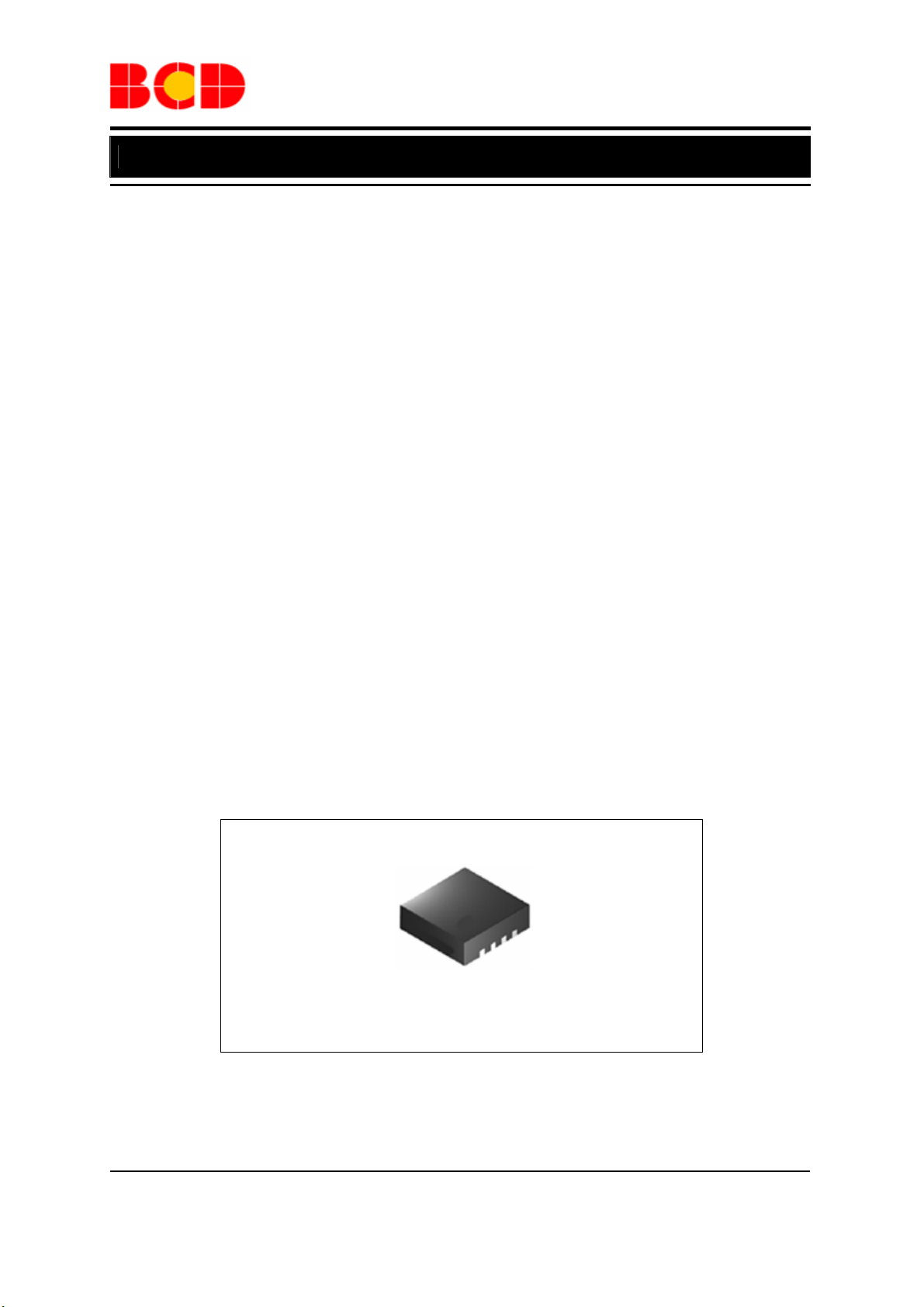
DFN-3×3-8
Figure 1. Package Type of AUR9716
Apr. 2012 Rev. 1. 0 BCD Semiconductor Manufacturing Limited
1
Data Sheet
1.0MHz to 1.4MHz, 2A, STEP DOWN DC-DC CONVERTER AUR9716
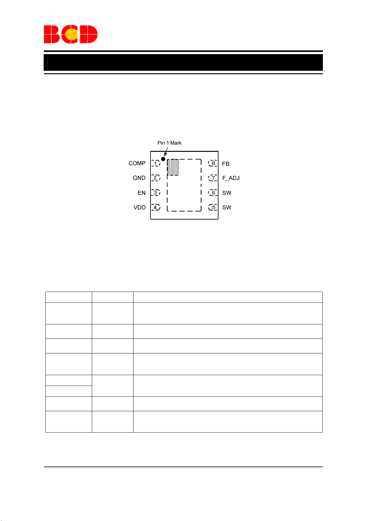
Pin Configuration
D Package
(DFN-3×3-8)
Figure 2. Pin Configuration of AUR9716 (Top View)
Pin Description
Pin Number Pin Name Function
Compensation Point. COMP is used to compensate the regulation control
1 COMP
2 GND
3 EN
4 VDD
5
SW
6
7 F_ADJ
8 FB
loop. Connect R and C from COMP and GND to compensate the regulation
control loop
Ground. The exposed pad is soldered to PCB and connected to GND plant
for good power dissipation
Enable Input. EN is an input when the regulator on or off. When left
unconnected, EN pin is pulled to VDD by the internal pull up resistor
Power input V
ceramic bypass capacitor between VDD and GND to eliminate input
noise and ripple voltage
Switch Output. SW is the switching point which supplies voltage and
current to output
Oscillator Resistor Input. Connecting a resistor to ground from this pin sets
the switching frequency
Feedback Input. Receives the feedback voltage from a resistive divider
connected across the output. The feedback reference voltage is 0.8V
typically
provides the input power to the regulator. Connecting a
IN
Apr. 2012 Rev. 1. 0 BCD Semiconductor Manufacturing Limited
2
Data Sheet
1.0MHz to 1.4MHz, 2A, STEP DOWN DC-DC CONVERTER AUR9716
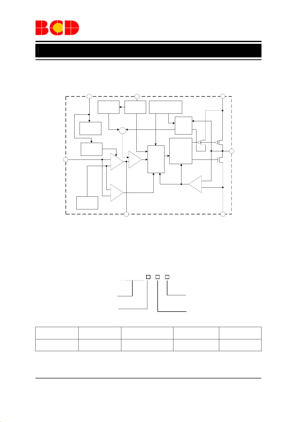
Functional Block Diagram
EN
FB
3
Generator
8
Bandgap
Reference
Saw-tooth
Generator
Bias
Soft
Start
Over Voltage
Comparator
Figure 3. Functional Block Diagram of AUR9716
Ordering Information
Circuit Type
A: Adjustable Output
Package
Temperature
Range
F_ADJ
7
Oscillator
+
-
+
Error
Amplifier
+
-
Modulator
Control
-
+
1
COMP
AUR9716
Part Number Marking ID Packing Type
Over-Current
Comparator
Buffer &
Dead Time
Control
Logic
Reverse Inductor
Current Comparator
Current
Sensing
Logic
VDD
4
-
+
2
GND
Package
D: DFN-3×3-8
G: Green
5, 6
SW
DFN-3×3-8 -40 to 80°C AUR9716AGD 9716A Tape & Reel
BCD Semiconductor's Pb-free products, as designated with "G" in the part number, are RoHS compliant and
green.
Apr. 2012 Rev. 1. 0 BCD Semiconductor Manufacturing Limited
3
Data Sheet
1.0MHz to 1.4MHz, 2A, STEP DOWN DC-DC CONVERTER AUR9716
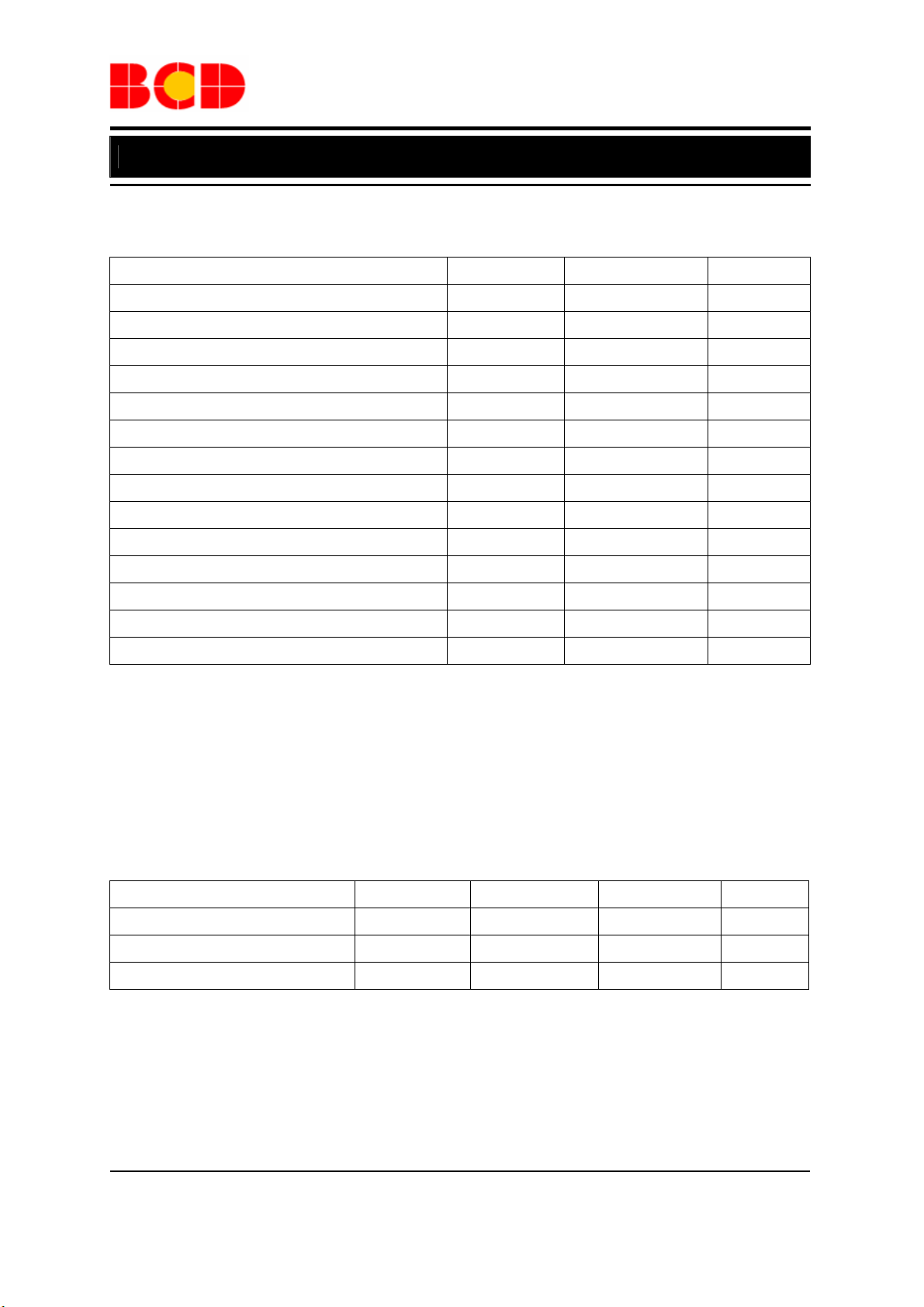
Absolute Maximum Ratings (Note 1)
Parameter Symbol Value Unit
Supply Input Voltage
SW Pin Switch Voltage
Output Voltage
P-MOSFET Switch Source Current I
N-MOSFET Switch Sink Current I
Power Dissipation (on PCB, TA=25°C)
Package Thermal Resistance (Junction to Ambient)
Package Thermal Resistance (Junction to Case)
Lead Temperature (Soldering, 5sec)
Junction Temperature
Operating Temperature Range
Storage Temperature Range
ESD (Human Body Model)
ESD (Machine Model)
V
IN
V
SW
V
EN
3.5 A
SW-P
3.5 A
SW-N
P
D
θ
JA
θ
JC
T
LEAD
T
J
T
OP
T
STG
V
HBM
VMM
-0.3 to 6.0 V
-0.3 to V
-0.3 to V
-40 to 85 °C
-55 to 150 °C
+0.3 V
IN
+0.3 V
IN
2.56 W
39.13 °C/W
3.39 °C/W
260 °C
150 °C
2000 V
200 V
Note 1: Stresses greater than those listed under “Absolute Maximum Ratings” may cause permanent damage to
the device. These are stress ratings only, and functional operation of the device at these or any other conditions
beyond those indicated under “Recommended Operating Conditions” is not implied. Exposure to “Absolute
Maximum Ratings” for extended periods may affect device reliability.
Recommended Operating Conditions
Parameter Symbol Min Max Unit
Supply Input Voltage VIN 2.5 5.5 V
Junction Temperature Range TJ -20 125 °C
Operating Temperature Range TA -40 80 °C
Apr. 2012 Rev. 1. 0 BCD Semiconductor Manufacturing Limited
4
Data Sheet
1.0MHz to 1.4MHz, 2A, STEP DOWN DC-DC CONVERTER AUR9716
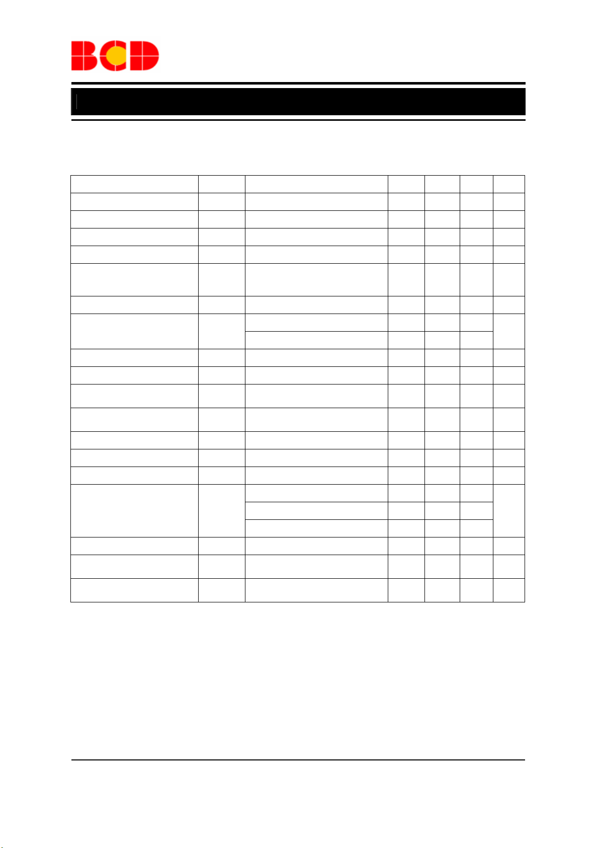
Electrical Characteristics
VIN=5V, VFB=0.8V, f
Parameter Symbol Test Condition Min Typ Max Unit
=1.4MHz, L=1.5µH, CIN=10µF, C
OSC
=10µF, TA=25°C, unless otherwise specified.
OUT
Input Voltage Range
Shutdown Current
Active Current
Regulated Feedback Voltage
Regulated Output Voltage
Peak Inductor Current
Oscillator Frequency
P_MOSFET RON
N_MOSFET RON
EN Input High-Threshold
Voltage
EN Input Low-Threshold
Voltage
EN Input Current
Soft-start Time
Maximum Duty Cycle
Under Voltage Lock Out
Threshold
V
I
ION
VFB
∆V
/V
IPK
f
OSC
R
DSON(P)
R
DSON(N)
V
V
IEN
tSS
D
V
UVLO
IN
OFF
OUT
OUT
ENH
ENL
MAX
2.5 5.5 V
VEN=0V 0.1 1 µA
VFB=0.95V 460 µA
For adjustable output voltage 0.784 0.8 0.816 V
VIN=2.5V to 5.5V,
I
=0A to 2A
OUT
-3 3 %
VFB=0.7V 2.2 3.2 3.7 A
R
=5.1MΩ 1.12 1.4 1.68
OSC
Adjustable switching frequency 1.0 1.4
ISW=0.5A 90 110 130 mΩ
ISW=0.5A 90 110 130 mΩ
Enable Threshold 1.5 V
Shutdown Threshold 0.4 V
MHz
2 µA
800 µs
100 %
VIN Rising 2.4
VIN Falling 2.3
V
Hysteresis 0.1
Thermal Shutdown TSD Hysteresis=30°C 150 °C
Error Amplifier Trans
Conductance
Current Sense Trans
Resistance
g
3000 µs
m
R
5 Ω
T
Apr. 2012 Rev. 1. 0 BCD Semiconductor Manufacturing Limited
5
 Loading...