Diodes AUR9703 User Manual

1.5MHz, 800mA, STEP DOWN DC-DC CONVERTER AUR9703
Data Sheet
General Description
The AUR9703 is a high efficiency step-down
DC-DC voltage converter. The chip operation is
optimized using constant frequency, peak-current
mode architecture with built-in synchronous power
MOSFET switchers and internal compensators to
reduce external part counts. It is automatically
switching between the normal PWM mode and LDO
mode to offer improved system power efficiency
covering a wide range of loading conditions.
The oscillator and timing capacitors are all built-in
providing an internal switching frequency of 1.5MHz
that allows the use of small surface mount inductors
and capacitors for portable product implementations.
Additional features included Soft Start (SS), Under
Voltage Lock Out (UVLO), and Thermal Shutdown
Detection (TSD) to provide reliable product
applications.
The device is available in adjustable output voltage
versions ranging from 1V to 3.3V, and is able to
deliver up to 800mA.
The AUR9703 is available in TSOT-23-5 package.
Features
• High Efficiency Buck Power Converter
• Low Quiescent Current
• Output Current: 800mA
• Adjustable Output Voltage from 1V to 3.3V
• Wide Operating Voltage Range: 2.5V to 5.5V
•
Built-in Power Switches for Synchronous
Rectification with High Efficiency
• Feedback Voltage: 600mV
• 1.5MHz Constant Frequency Operation
• Automatic PWM/LDO Mode Switching Control
• Thermal Shutdown Protection
• Low Drop-out Operation at 100% Duty Cycle
• No Schottky Diode Required
Applications
• Mobile Phone, Digital Camera and MP3 Player
• Headset, Radio and Other Hand-held Instrument
• Post DC-DC Voltage Regulation
• PDA and Notebook Computer
TSOT-23-5
Figure 1. Package Type of AUR9703
Nov. 2011 Rev. 1 .0 BCD Semiconductor Manufacturing Limited
1

Data Sheet
1.5MHz, 800mA, STEP DOWN DC-DC CONVERTER AUR9703
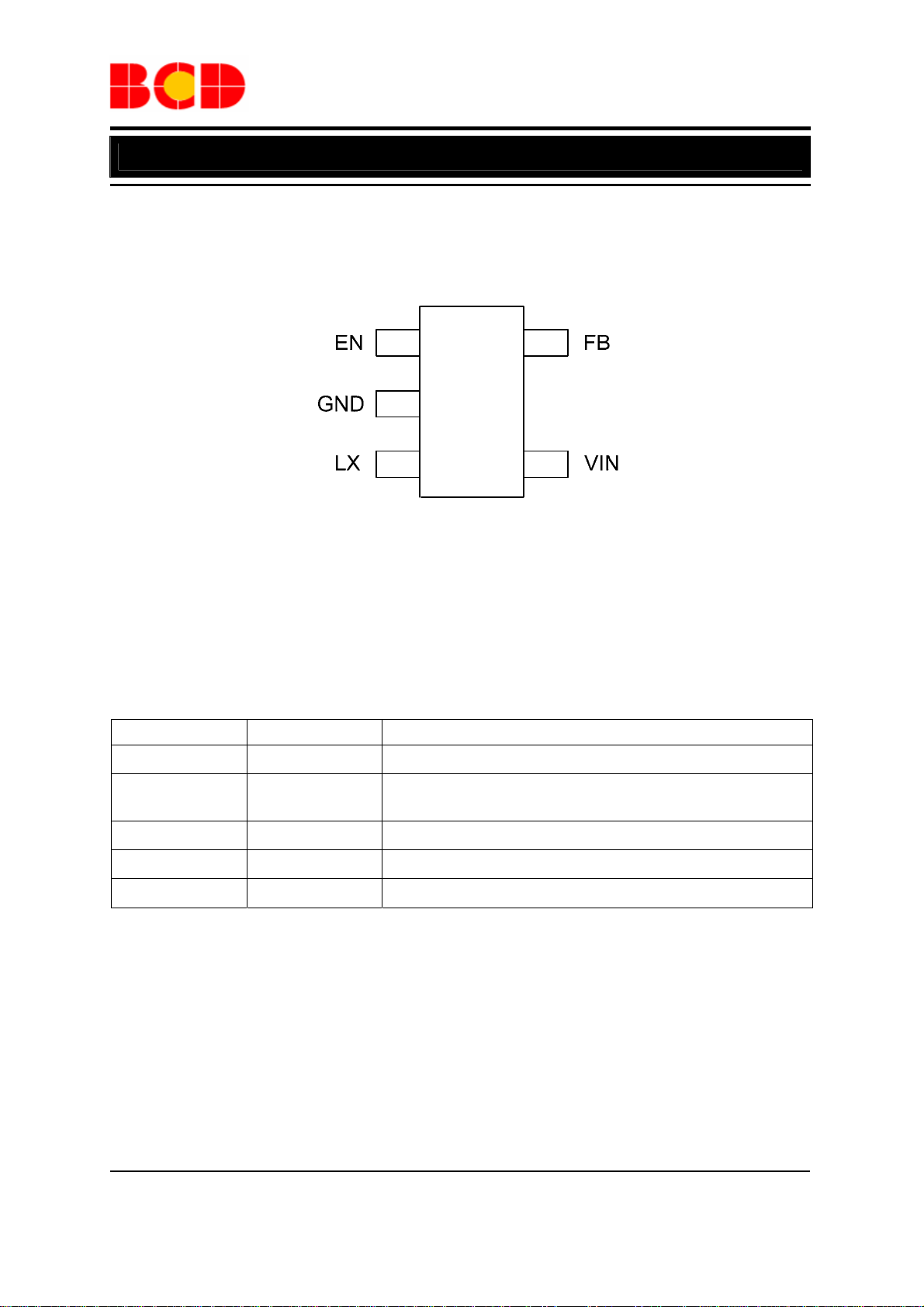
Pin Configuration
H Package
(TSOT-23-5)
1
5
2
34
Figure 2. Pin Configuration of AUR9703 (Top View)
Pin Description
Pin Number Pin Name Function
1 EN Enable signal input, active high
2 GND
This pin is the GND reference for the NMOS power stage. It
must be connected to the system ground
3 LX Connect to inductor
4 VIN Power supply input
5 FB Feedback voltage from the output
Nov. 2011 Rev. 1 .0 BCD Semiconductor Manufacturing Limited
2

Data Sheet
1.5MHz, 800mA, STEP DOWN DC-DC CONVERTER AUR9703
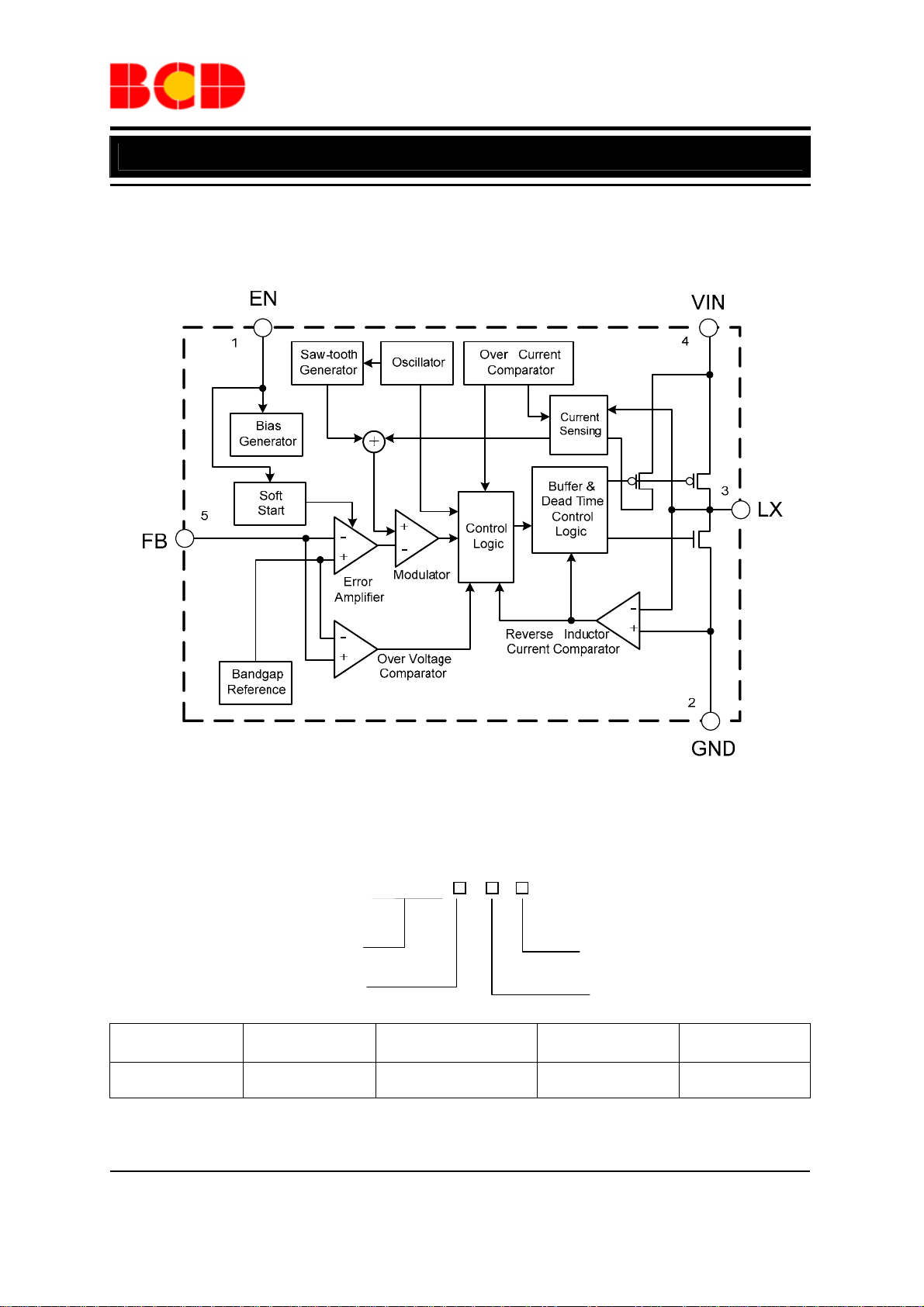
Functional Block Diagram
Figure 3. Functional Block Diagram of AUR9703
Ordering Information
AUR9703 A
Circuit Type
A: Adjustable Output
5
Package
TSOT-23-5 -40 to 80°C AUR9703AGH 9703AG Tape & Reel
Temperature
Range
Part Number Marking ID Packing Type
BCD Semiconductor's Pb-free products, as designated with "G" in the part number, are RoHS compliant and
green.
Nov. 2011 Rev. 1 .0 BCD Semiconductor Manufacturing Limited
3
Package
H: TSOT-23-5
G: Green

Data Sheet
1.5MHz, 800mA, STEP DOWN DC-DC CONVERTER AUR9703
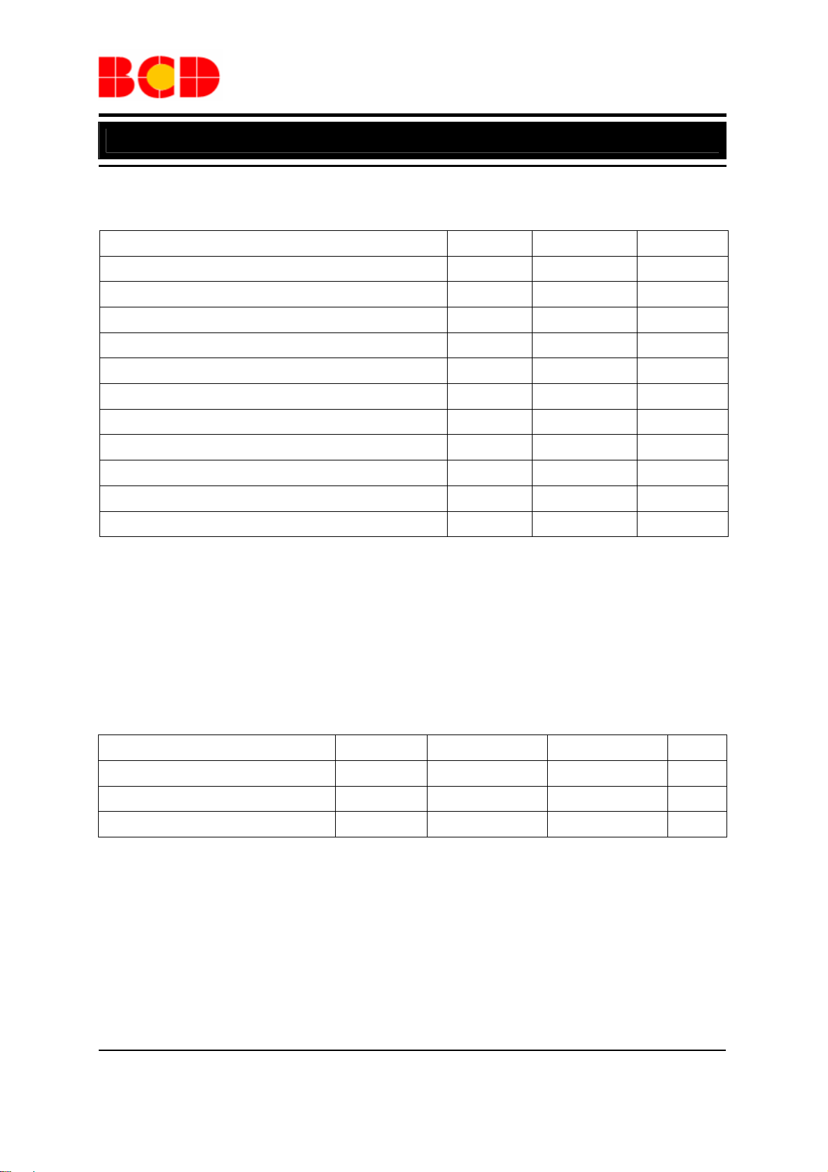
Absolute Maximum Ratings (Note 1)
Parameter Symbol Value Unit
Supply Input Voltage VIN
Enable Input Voltage VEN
Output Voltage V
Power Dissipation (On PCB, TA=25°C) PD
Thermal Resistance (Junction to Ambient, Simulation) θJA
Thermal Resistance (Junction to Case, Simulation) θJC
Operating Junction Temperature TJ
Operating Temperature TOP
Storage Temperature T
ESD (Human Body Model) V
ESD (Machine Model) VMM
Note 1: Stresses greater than those listed under “Absolute Maximum Ratings” may cause permanent damage to
the device. These are stress ratings only, and functional operation of the device at these or any other conditions
beyond those indicated under “Recommended Operating Conditions” is not implied. Exposure to “Absolute
Maximum Ratings” for extended periods may affect device reliability.
OUT
STG
HBM
0 to 6.0
-0.3 to VIN+0.3
-0.3 to VIN+0.3
0.85
118.31
113.67
160
-40 to 85
-55 to 150
2000
200
V
V
V
W
°C/W
°C/W
°C
°C
°C
V
V
Recommended Operating Conditions
Parameter Symbol Min Max Unit
Supply Input Voltage VIN 2.5 5.5 V
Junction Temperature Range TJ -20 125 °C
Ambient Temperature Range TA -40 80 °C
Nov. 2011 Rev. 1 .0 BCD Semiconductor Manufacturing Limited
4

Data Sheet
1.5MHz, 800mA, STEP DOWN DC-DC CONVERTER AUR9703
Electrical Characteristics
VIN=5V, V
otherwise specified.
Parameter Symbol Conditions Min Typ Max Unit
Input Voltage Range VIN 2.5 5.5 V
=3.3V, VFB=0.6V, L=2.2µH, CIN=4.7µF, C
OUT
=10µF, TA=25°C, I
OUT
=800mA. Unless
MAX
Shutdown Current I
Regulated1Feedback
Voltage
Regulated Output
Voltage Accuracy
∆V
Peak Inductor
Current
Oscillator Frequency f
PMOSFET RON R
NMOSFET RON R
Quiescent Current IQ I
LX Leakage Current ILX
V
OFF
For Adjustable Output Voltage 0.585 0.6 0.615 V
V
FB
OUT/VOUT
I
OSC
ON(P)
ON(N)
V
PK
V
VIN=5V, I
VIN=5V, I
=0 0.1 1 µA
EN
=2.5V to 5.5V,
V
IN
=0 to 800mA
I
OUT
=5V, VFB=0.5V 1.2 A
IN
=5V 1.2 1.5 1.8 MHz
IN
=200mA 0.25 Ω
OUT
=200mA 0.27 Ω
OUT
=0A, VFB= 0.7V 100 µA
OUT
=0V, VLX=0V or 5V,
V
EN
=5V
V
IN
-3 3 %
0.1 1 µA
Feedback Current IFB 30 nA
Soft Start Time tSS 200 µs
EN Leakage Current IEN 0.01 0.1 µA
EN High-level Input
Voltage
EN Low-Level Input
Voltage
V
V
EN_H
V
V
EN_L
=2.5V to 5.5V 1.5 V
IN
=2.5V to 5.5V 0.6 V
IN
Under Voltage Lock
Out
1.8 V
V
UVLO
Hysteresis 0.1 V
Thermal Shutdown TSD 160 °C
Nov. 2011 Rev. 1 .0 BCD Semiconductor Manufacturing Limited
5

Data Sheet
1.5MHz, 800mA, STEP DOWN DC-DC CONVERTER AUR9703
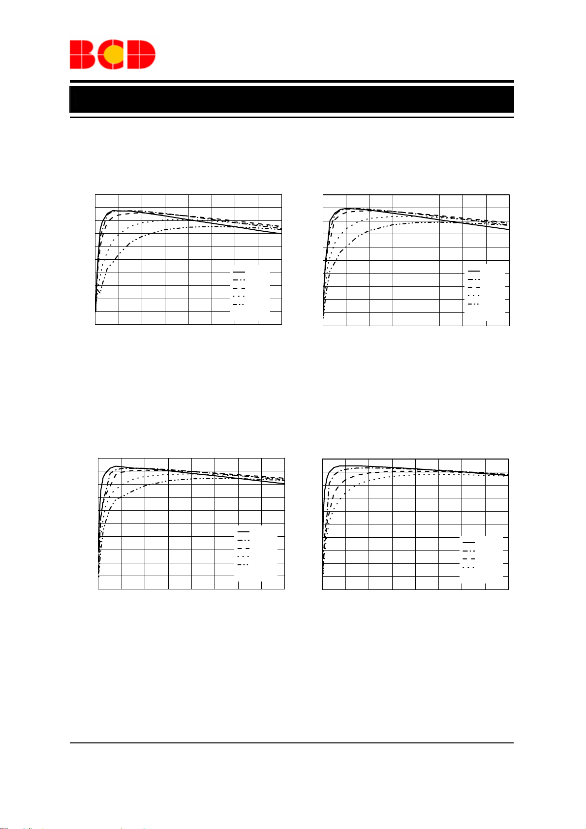
Typical Performance Characteristics
100
90
80
70
60
50
40
30
Efficiency (%)
20
10
0
0.0 0.1 0.2 0.3 0.4 0.5 0.6 0.7 0.8
Output Current (A)
V
OUT
VIN=2.5V
VIN=3.3V
VIN=4.2V
VIN=5.0V
VIN=5.5V
=1.0V
Figure 4. Efficiency vs. Output Current (V
=1.0V) Figure 5. Efficiency vs. Output Current (V
OUT
100
90
80
70
60
50
40
30
Efficiency (%)
20
10
0
0.0 0.1 0.2 0.3 0.4 0.5 0.6 0.7 0.8
Output Current (A)
Figure 6. Efficiency vs. Output Current (V
VIN = 2.5V
VIN = 3.3V
VIN = 4.2V
VIN = 5.0V
VIN = 5.5V
V
=1.8V
OUT
=1.8V) Figure 7. Efficiency vs. Output Current (V
OUT
100
90
80
70
60
50
40
30
Efficiency (%)
20
10
0
0.0 0.1 0.2 0.3 0.4 0.5 0.6 0.7 0.8
V
OUT
Output Current (A)
OUT
100
90
80
70
60
50
40
30
Efficiency (%)
20
V
10
0
0.0 0.1 0.2 0.3 0.4 0.5 0.6 0.7 0.8
=2.5V
OUT
Output Current (A)
OUT
VIN=2.5V
VIN=3.3V
VIN=4.2V
VIN=5.0V
VIN=5.5V
=1.2V
=1.2V)
VIN = 3.3V
VIN = 4.2V
VIN = 5.0V
VIN = 5.5V
=2.5V)
Nov. 2011 Rev. 1 .0 BCD Semiconductor Manufacturing Limited
6
 Loading...