Diodes AUR3852 User Manual

Data Sheet
Enhanced Multi-touch Capacitive Touch Screen Controller AUR3852
General Description
The AUR3852 is a low-cost high-resolution single
chip solution for APA capacitive touch screen. It is
an 8-bit single cycle 8051 microcontroller with ICP
Interface. The chip includes a 12-bit successive
approximation analog-to-digital converter with an I
2
interface and multiplexer-switcher circuits for
flexible measurement of analog signal from APA
panel. An accurate switched-capacitor integrator is
built-in and it can auto calibrate the pixel parameters
for a wide range of capacitance on the touch screen
(0.1pF to 4pF). On-chip capacitor can replace
external component. This touch screen controller
(TSC) with CMOS integration circuit provides an
ideal choice for APA touch panel. The AUR3852 is
specified over the temperature range of -40°C to
85°C.
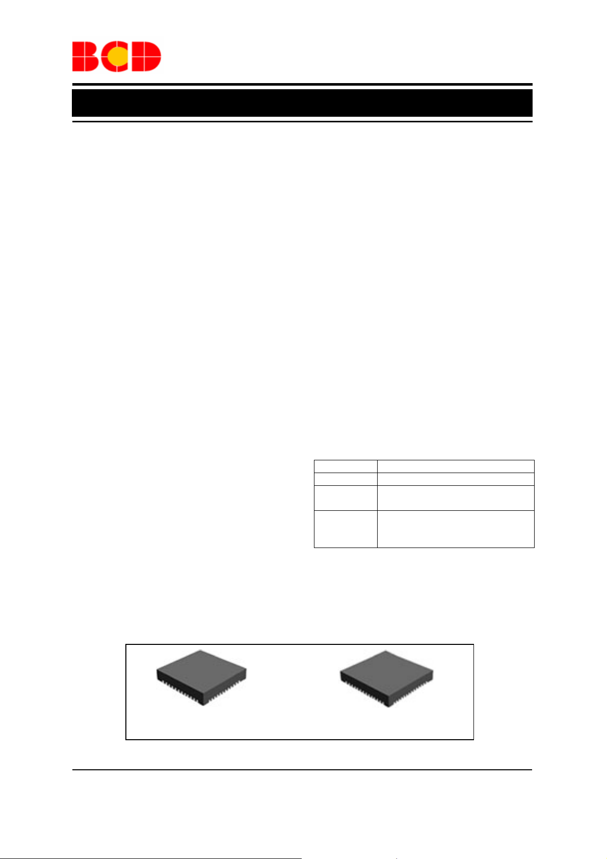
The AUR3852 is available in QFN-6×6-48 and
QFN-7×7-56 packages.
Features
•
1Mutual Capacitive Touch Sensing
• Single Power Supply: 2.8V to 3.6V Operation
Voltage
•
1Supports Low Voltage to 1.8V by Built-in 1.8V
to 3.3V Boost Converter
• QFN-6×6-48 Package: Up to 20 Drive Lines and
14 Sense Lines
•
1QFN-7×7-56 Package: Up to 27 Drive Lines and
15 Sense Lines
•
1Dedicated Internal Two-wire Serial Control Bus
2
I
C and UART between AUR3852 and Host
•
1Single-end Integrator with Programmable Gain
Control and Offset Control
•
1Multiplexed Analog Digitization with 12-bit
Resolution SAR ADC
QFN-6×6-48
Feb. 2013 Rev. 1. 0 BCD Semiconductor Manufacturing Limited
Figure 1. Package Types of AUR3852
Features (Continued)
• Single Cycle 8051 CPU Core, Maximum Operating Clock up to 24MHz from IOSC
2MHz to 24MHz Internal Oscillator (IOSC)
32K-byte Flash ROM
C
256-byte Internal SRAM and 5888-byte
XSRAM
Two 16-bit Timers T0/T1 and One 16-bit ECT
Timer T2
2
One I
C Slave Controller and One I2C Master
Controller Shared with the Same Port
With Asynchronous I
2
C Slave Address
Detection Logic Design
Up to 30 General Purpose GPIO Pins (QFN-56);
25 General Purpose GPIO Pins (QFN-48)
Up to 8 External Interrupt Pins
Up to 2 UART Ports (QFN-56); 1 UART Port
(QFN-48)
• ISP/IAP via I²C/UART Port
(With External Clock I/O Pin Definition for
UART IAP. Pin Shared with P1.7)
• Operation Temperature Range: -40°C to 85°C
• Package Typ e: QFN-6×6-48 and QFN-7×7-56
• RoHS Compliance
• O perating Mode:
Mode Description
Power-down No scan with power-down mode
Low speed Lower scan rate when finger is not
on panel, IOSC=32kHz
Standard Higher scan rate when fingers are
on panel, IOSC can up to 2MHz
to 24MHz
Applications
• Mobile Phones
• Personal Digital Assistants
• Smart Hand-held or Gaming Devices
1
QFN-7×7-56

Data Sheet
Enhanced Multi-touch Capacitive Touch Screen Controller AUR3852
Pin Configuration
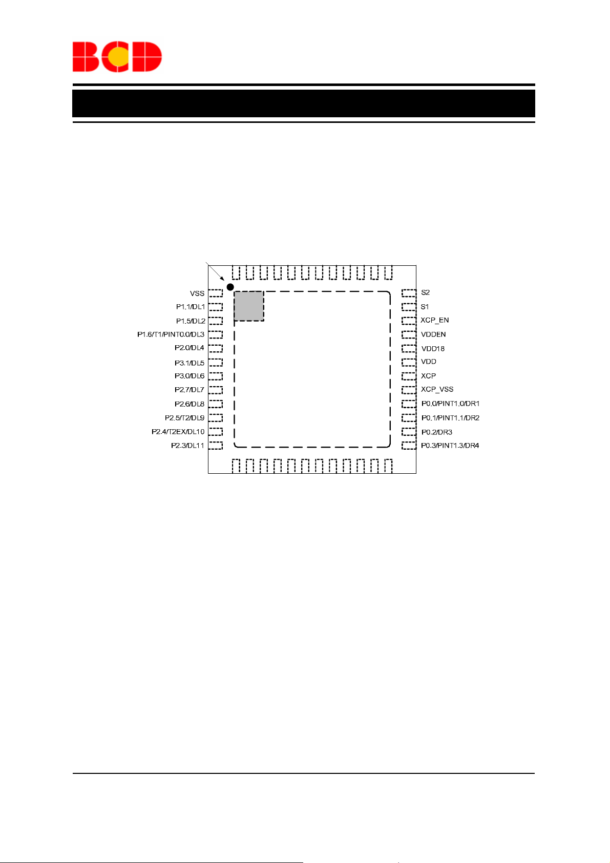
QT Package
(QFN-6×6-48)
Pin 1 Mark
S13
S14
48
47
S10
S11
S12
S9
S8
4243444546
S7
S5
S6
39
4041
S4
S3
3738
1
2
3
4
5
6
7
8
9
10
11
12
15 161413
RSTN
P2.2/TXD1
P3.6/RXD1
EP
17 18 19 20 21 22 23 24
TESTEN
P1.3/SCL
P1.2/SDA
P1.0/DR9
P0.6/TXD0/DR7
P0.7/RXD0/DR8
P1.7/T0/PINT0.1/EXTCLKIN
P0.5/PINT1.5/DR6
36
35
34
33
32
31
30
29
28
27
26
25
P0.4/PINT1.4/DR5
Feb. 2013 Rev. 1. 0 BCD Semiconductor Manufacturing Limited
2

Data Sheet
Enhanced Multi-touch Capacitive Touch Screen Controller AUR3852
Pin Configuration (Continued)
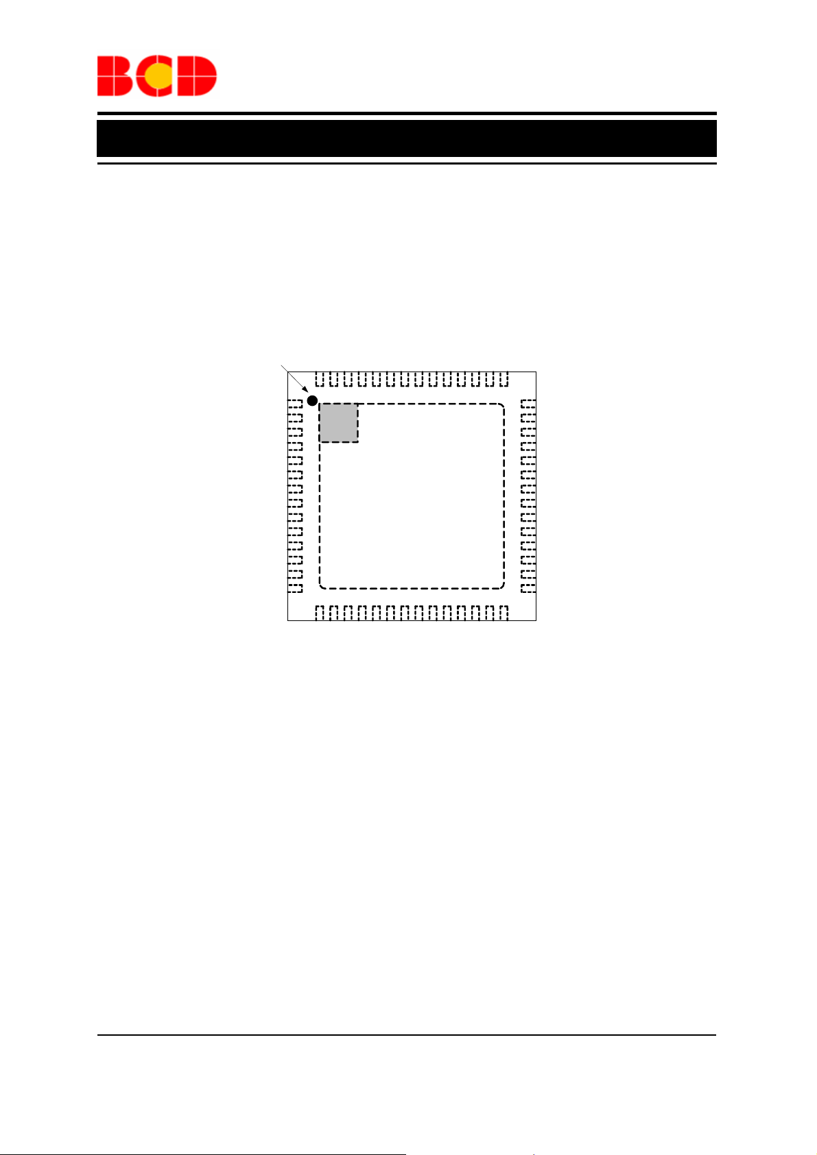
QU Package
(QFN-7×7-56)
Pin 1 Mark
VSS
P1.1/DL1
P1.5/DL2
P1.6/T1/PINT0.0/DL3
P2.0/DL4
P3.1/DL5
P3.0/DL6
P2.7/DL7
P2.6/DL8
P2.5/T2/DL9
P2.4/T2EX/DL10
P2.3/DL11
P3.2/DL12
P3.3/DL13
S14
RSTN
P1.3/SCL
S12
S13S9S10
EP
TESTEN
P1.2/SDA
P1.7/T0/PINT0.1/EXTCLKIN
S15
XDX0
XDX1
56
1
2
3
4
5
6
7
8
9
10
11
12
13
14
17 18 19 20 21 22 23 24 25 26 27 28
15
16
P2.2/TXD1
P3.6/RXD1
S11
S7
S5
S6
S8
P3.5/DR11
P1.4/DR10
P3.4/DR12
S4
43444546474849505152535455
42
S3
41
S2
40
S1
39
XCP_EN
38
VDDEN
37
VDD18
36
VDD
35
XCP
34
XCP_VSS
33
P0.0/PINT1.0/DR1
32
P0.1/PINT1.1/DR2
31
P0.2/DR3
30
P0.3/PINT1.3/DR4
29
P0.4/PINT1.4/DR5
P1.0/DR9
P0.6/TXD0/DR7
P0.7/RXD0/DR8
P0.5/PINT1.5/DR6
Figure 2. Pin Configuration of AUR3852 (Top View)
Feb. 2013 Rev. 1. 0 BCD Semiconductor Manufacturing Limited
3

t
g
Data Sheet
Enhanced Multi-touch Capacitive Touch Screen Controller AUR3852
Pin Description
Pin Number
QFN-6×6-
48
1 1 VSS Power Ground Voltage. 0V
2 2 P1.1 I/O
3 3 P1.5 I/O
4 4 P1.6 I/O
5 5 P2.0 I/O
6 6 P3.1 I/O
7 7 P3.0 I/O, A
QFN-7×7-
56
Pin
Name
Pin
Type
Pin Function
Port 1.1 GPIO
8051 P1.1 GPIO
DL1
Left driving line 1
Port 1.5 GPIO
8051 P1.5 GPIO
DL2
Left driving line 2
Port 1.6 GPIO
8051 P1.6 GPIO
PINT0.0
This pin can alsobe configured as the expanded INT0
interrup
T1 Timer 1 Input
This pin can also be configured as Timer 1 input
DL3
Left driving line 3
Port 2.0 GPIO
8051 P2.0 GPIO. To allow proper operation as GPIO P2.0
function, crystal oscillator must be disabled by setting
XOSCCFG re
DL4
Left driving line 4
Port 3.1 GPIO
8051 P3.1 GPIO
DL5
Left driving line 5
Port 3.0 GPIO
8051 P3.0 GPIO
DL6
Left driving line 6
ister to 0x00
Feb. 2013 Rev. 1. 0 BCD Semiconductor Manufacturing Limited
4

g
Data Sheet
Enhanced Multi-touch Capacitive Touch Screen Controller AUR3852
Pin Description (Continued)
Pin Number
QFN-6×6-
48
8 8 P2.7 I/O
9 9 P2.6 I/O
10 10 P2.5 I/O
11 11 P2.4 I/O
12 12 P2.3 I/O
13 15 P3.6 I/O
14 16 P2.2 I/O
Feb. 2013 Rev. 1. 0 BCD Semiconductor Manufacturing Limited
QFN-7×7-
56
Pin
Name
Pin
Type
Pin Function
Port 2.7 GPIO
8051 P2.7 GPIO
DL7
Left driving line 7
Port 2.6 GPIO
8051 P2.6 GPIO
DL8
Left driving line 8
Port 2.5 GPIO
8051 P2.5 GPIO
T2 Timer 2 Input
This pin can also be configured as Timer 2 input
DL9
Left driving line 9
Port 2.4 GPIO
8051 P2.4 GPIO
T2EX Timer 2 Trigger
This pin can also be configured as T2EX signal for Timer
2. T2EX is the Timer 2 trigger input
DL10
Left driving line 10
Port 2.3 GPIO
8051 P2.3 GPIO
DL11
Left driving line 11
Port 3.6 GPIO
8051 P3.6 GPIO
RXD1
This pin can also be configured as RXD of UART 1
Port 2.2 GPIO
8051 P2.2 GPIO.
TXD1
This pin can also be configured as TXD of UART 1
8051 P2.2 GPIO. To allow proper operation as GPIO P2.2
function, crystal oscillator must be disabled by setting
XOSCCFG re
5
isterto 0x00

t
t
Data Sheet
Enhanced Multi-touch Capacitive Touch Screen Controller AUR3852
Pin Description (Continued)
Pin Number
QFN-6×6-
48
15, 18 17, 20
16 18 P1.3 I/O
17 19 P1.2 I/O
19 21 P1.7 I/O
20 25 P1.0 I/O
21 26 P0.7 I/O
QFN-7×7-
56
Pin
Name
RSTN,
TESTE
N
Pin
Type
I
Pin Function
Reset Low Active
Typically connect a resistor to VDD and a capacitor to
VSS
Low asserted and threshold at 0.5×VDD. When forced low,
the chip enters into reset condition
This pin should not be connected to any level above VDD
Port 1.3 GPIO
8051 P1.3 GPIO
SCL
This pin can alsobe configured as the SCL signal of the
2
C master or I2C slave controller. In I2C master mode, this
I
pin should be configured as open-drain output. In I
slave mode, this pin should be configured as input only
Port 1.2 GPIO
8051 P1.2 GPIO
SDA
This pin can alsobe configured as the SDA signal of the
2
C master or I2C slave controller. In this operation mode,
I
this pin should also be configured as bi-directional I/O
with open-drain outpu
Port 1.7 GPIO
8051 P1.7 GPIO
PINT0.1
This pin can also be configured as the expanded INT0
interrup
T0 Timer 0 Input
This pin can also be configured as Timer 0 input
External Clock Input
External clock input source
Port 1.0 GPIO
8051 P1.0 GPIO
DR9
Right driving line 9
Port 0.7 GPIO
8051 P0.7 GPIO
RXD0
This pin can also be configured as RXD of UART 0
DR8
Right driving line 8
2
C
Feb. 2013 Rev. 1. 0 BCD Semiconductor Manufacturing Limited
6
 Loading...