

Page 1
ATS137
SINGLE HALL EFFECT SWITCH
Features
• 3.5V to 20V DC Operation Voltage
• Temperature Compensation
• Wide Operating Voltage Range
• Open-Collector Pre-Driver
• 25mA Maximum Sinking Output Current
• Reverse Polarity Protection
• Lead Free Package: SIP-3L and SC59-3L
known as SOT23 in Asia)
• SIP-3L and SC59-3L: Available in “Green” Molding
Compound (No Br, Sb)
• Lead Free Finish / RoHS Compliant (Note 1)
Applications
• VCD/DVD Loader, CD/DVD ROM
• Cover Detector
• Speed Measurement
• Home Appliances
• Home Safety
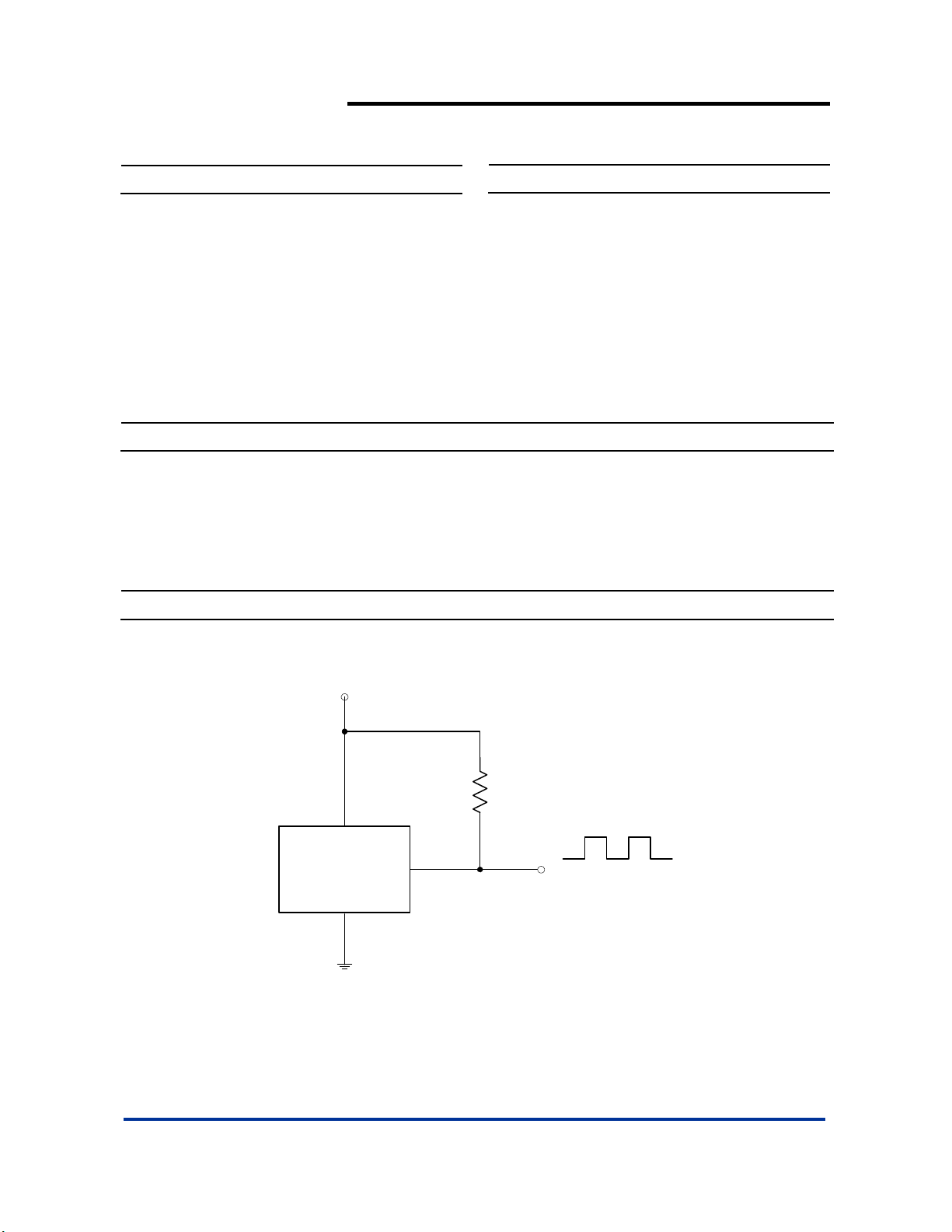
Typical Application Circuit
(Commonly
General Description
ATS137 is a switched Hall-Effect IC, which is for contactless
switching applications. The device includes an on-chip Hall
voltage generator for magnetic sensing, an amplifier that
amplifies the Hall voltage, a Schmitt trigger to provide switching
hysteresis for nois e rejection, a nd an open-coll ector output. Th e
bandgap regulator allows a wide operating voltage range.
ATS137 is rated for operating temperature range from -20°C to
85°C and voltage range from 3.5V to 20V.
3.5V ~20V
R
V
cc
L
DO
ATS137
Digital Output
GND
ATS137 Rev. 10 1 of 12 FEBRUARY 2010
DS31045
www.diodes.com © Diodes Incorporated
Page 2
Ordering Information
ATS137
SINGLE HALL EFFECT SWITCH
Package
P : SIP-3L
W : SC59-3L
ATS 137 - X X - X - X
Lead Free
L : Lead Free
G : Green
Packing
A : Ammo Box (Note 3)
B : Bulk (Note 4)
Magnetic
Characteristics
A or B (Note 5)
7 : Tape & Reel
Device
ATS137-PL-A-A P SIP-3L NA NA NA NA 4000/Box -A A
ATS137-PL-A-B P SIP-3L NA NA NA NA 4000/Box -A B
ATS137-PL-B-A P SIP-3L 1000 -B NA NA NA NA A
ATS137-PL-B-B P SIP-3L 1000 -B NA NA NA NA B
ATS137-PG-A-A P SIP-3L NA NA NA NA 4000/Box -A A
ATS137-PG-A-B P SIP-3L NA NA NA NA 4000/Box -A B
ATS137-PG-B-A P SIP-3L 1000 -B NA NA NA NA A
ATS137-PG-B-B P SIP-3L 1000 -B NA NA NA NA B
ATS137-WL-7-A W SC59-3L NA NA 3000/Tape & Reel -7 NA NA A
ATS137-WG-7-A W SC59-3L NA NA 3000/Tape & Reel -7 NA NA A
Notes: 1. EU Directive 2002/95/EC (RoHS). All applicable RoHS exemptions applied. Please visit our website at
2. Pad layout as shown on Diodes Inc. suggested pad layout document AP02001, which can be found on our website at
http://www.diodes.com/datasheets/ap02001.pdf.
3. Ammo Box is for SIP-3L Spread Lead.
4. Bulk is for SIP-3L Straight Lead.
5. Please refer the Magnetic Characteristics table, B is available in SIP-3L package only.
Package
http://www.diodes.com/products/lead_free.html
Code
Packaging
(Note 2)
Bulk 7” Tape and Reel Ammo Box
Quantity
Part
Number
Suffix
Quantity
Part
Number
Suffix
Quantity
Part
Number
Suffix
Characteristics
Magnetic
(Note 5)
Pin Assignment
(1) SIP-3L (2) SC59-3L
( Top View )
( Top View )
3.
DO
GND
2.
Vcc
1.
ATS137 Rev. 10 2 of 12 FEBRUARY 2010
DS31045
www.diodes.com © Diodes Incorporated
GND 2.
3. DO
1. Vcc
Page 3
)
Pin Descriptions
Pin Name Pin # Description
Vcc 1 Positive Power Supply
GND 2 Ground
DO 3 Digital Output
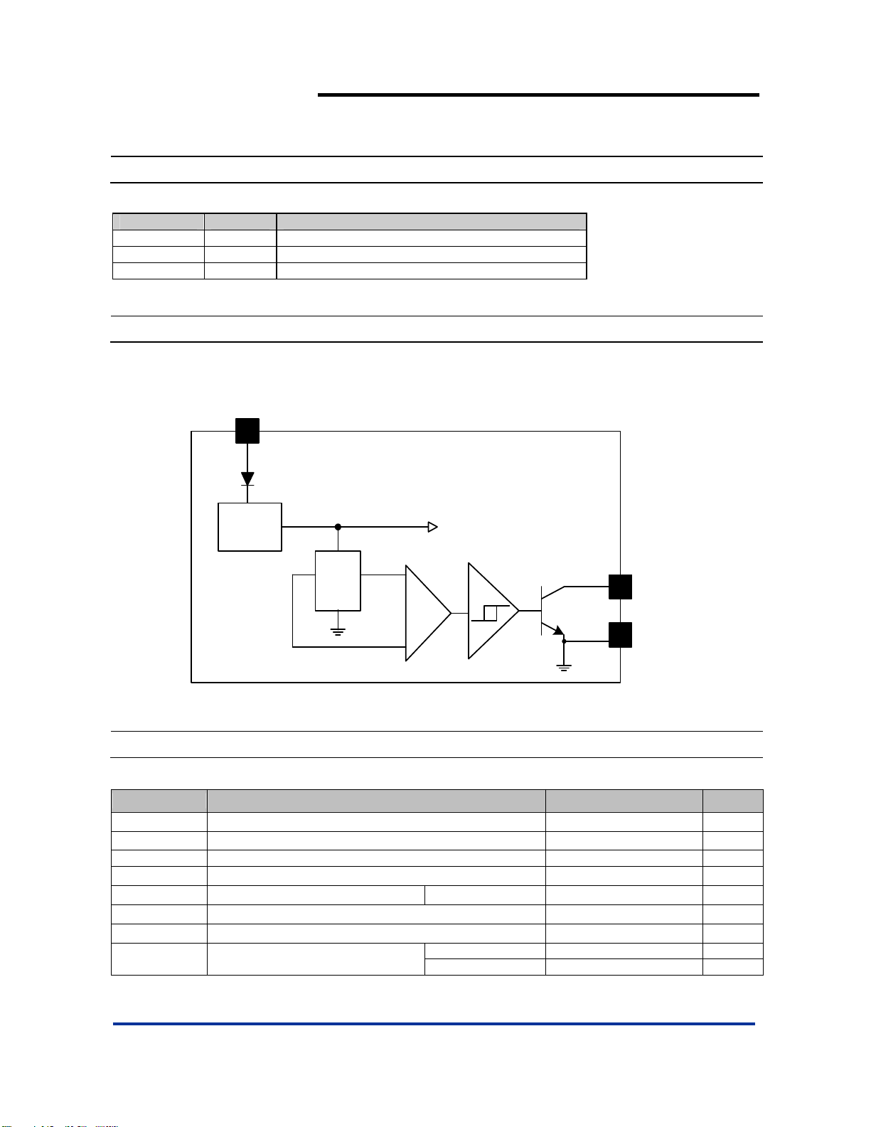
Functional Block Diagrams
V
CC
1
ATS137
SINGLE HALL EFFECT SWITCH
Regulator
Hall
Plate
Amp
Absolute Maximum Ratings (T
Symbol Characteristics Values Unit
VCC
V
RCC
B Magnetic Flux Density Unlimited
Vce
IC
TST
T
J(MAX
PD
ATS137 Rev. 10 3 of 12 FEBRUARY 2010
DS31045
Supply Voltage 20 V
Reverse VCC Polarity Voltage
Output “OFF” V oltage 30 V
Output “ON” Cu r r ent Continuous 25 mA
Storage Temperature -65~+150
Maximum Junction Temperature 150
Package Power Dissipation
= 25oC)
A
SIP-3L 550 mW
SC59-3L 230 mW
www.diodes.com © Diodes Incorporated
DO
3
2
GND
-20 V
°C
°C
Page 4
)
ATS137
SINGLE HALL EFFECT SWITCH
Recommended Operating Conditions
Symbol Characteristic Conditions Min Max Unit
VCC Supply Voltage Operating 3.5 20 V
TA Operating Ambient Temperature Operating -20 85
Electrical Characteristics (T
Symbol Characteristic Test Conditions Min Typ. Max Unit
V
Output Saturation Voltage VCC = 14V, ICC = 20mA - 300 700 mV
ce(SAT
I
Output Leakage Current Vce = 14V, VCC = 14V -
cex
ICC Supply Current VCC =20V, Output Open - 5 10 mA
tr Output Rise Time
tf Output Falling Time
= + 25°C)
A
V
= 14V, RL = 820Ω,
CC
CL = 20pF
V
= 14V, RL = 820Ω,
CC
CL = 20pF
<0.1
- 0.3 1.5 us
- 0.3 1.5 us
10 uA
°C
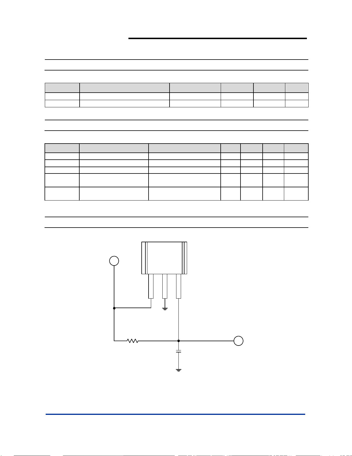
Test Circuit
14V
RL
RL = 820 Ohm
CL = 20 pF
CL
Test Circuit
DO
ATS137 Rev. 10 4 of 12 FEBRUARY 2010
DS31045
www.diodes.com © Diodes Incorporated
Page 5

ATS137
SINGLE HALL EFFECT SWITCH
Magnetic Characteristics (T
A grade
Symbol Parameter Min Typ. Max Unit
Bops(south pole to brand side) Operation Point - - 100 Gauss
Brps(south pole to brand side) Release Point 10 - - Gauss
Bhy( BrpxBopx − )
B grade (for SIP-3L only)
Symbol Parame ter Min Typ. Max Unit
Bops(south pole to brand side) Operation Point - - 130 Gauss
Brps(south pole to brand side) Release Point 10 - - Gauss
Bhy(
Notes: 7. Magnetic characteristics are for design information, which will vary with supply voltage, operating temperature and after soldering.
)
BrpxBopx −
Hysteresis - 80 - Gauss
Hysteresis - 80 - Gauss
= 25
A
o
C, Note 7)
(1mT = 10 Gauss)
ATS137 Rev. 10 5 of 12 FEBRUARY 2010
DS31045
www.diodes.com © Diodes Incorporated
Page 6

ATS137
SINGLE HALL EFFECT SWITCH
Application Information
Operating principle:
ATS137 is a three-pin Hall Effect switch IC which can turn magnetic flux variety to digital output signal. In other words, it is an interface
from magnetic system to an electrical one by Hall effect. The illustrations are shown in Fig.1.
V
O
V
CC
Turn Off
B
hys
Turn On
Magnet
S
Marking
Side
Vce(
Output driver is open-collector topology and maximum sink current (I
SAT
)
B
rp
B
op
Fig.1 Hall-Effect Switch
3.5 V ~20V
V
CC
DO
ATS137
I
sink
GND
Magnetic Flux
(Gauss)
) is 25mA. The illustrated circuit is shown as Fig. 2.
sink
R
L
Electrical
Vo
Digital Output
Fig.2 Application Circuit
ATS137 Rev. 10 6 of 12 FEBRUARY 2010
DS31045
www.diodes.com © Diodes Incorporated
Page 7

ATS137
SINGLE HALL EFFECT SWITCH
Application Information (Continued)
Vo will turn on (low) if the S magnetic flux larger than the operation point (Bop), and turns off whenever the magnetic flux is removed and
lower than the release point (B
). The related waveforms are shown in Fig.3.
rp
Magnetic Flux (mT)
B
op
S
Marking Side
N
(SC59)
S
N
(SIP3)
Marking Side
V
B
ce(SAT)
rp
V
O
V
CC
Fig.3 VO and Magnetic Flux Variety
The major applications are for contactless switching and shown as follows:
• VCD/DVD loader, CD/DVD ROM: Detect if the tray is opened or closed.
• Cover detector (open/close): Cellular phone cover detector, refrigerator door detector, microwave oven door sensor, etc.
• Home safety: instead of reed relay to detect the situation of door/window.
• Due to contactless and without mechanical contact point, its reliability and life cycle are much longer than reed relay. In
addition, its switching speed is much faster than mechanical devices.
t
t
ATS137 Rev. 10 7 of 12 FEBRUARY 2010
DS31045
www.diodes.com © Diodes Incorporated
Page 8

Performance Characteristics
(1) SIP-3L
TA (°C)
PD (mW)
TA (°C)
PD (mW)
P
(mW)
D
600
500
400
300
200
100
25 50 60 70 80 85 90 95 100
550 440 396 352 308 286 264 242 220
105 110 115 120 125 130 135 140 150
198 176 154 132 110 88 66 44 0
Power Dissipation Curve
ATS137
SINGLE HALL EFFECT SWITCH
0
0 25 50 75 100 125 150
(2) SC59-3L (commonly known as SOT23 i n Asia)
TA (°C)
PD (mW)
25 50 60 70 80 85 90 100 110 120 125 130 140 150
230 184 166 147 129 120 110 92 74 55 46 37 18 0
P
(mW)
D
300
200
100
0
0 2 5 50 75 100 12 5 150
P ower Dissipation C urve
85-40
TA (oC)
85-40
TA (oC)
ATS137 Rev. 10 8 of 12 FEBRUARY 2010
DS31045
www.diodes.com © Diodes Incorporated
Page 9

Marking Information
(1) SIP-3L
Part Number
( Top View )
137
Y
WW X
SINGLE HALL EFFECT SWITCH
: Year : 0~9
Y
WW
: Week : 01~52, "52" represents
52 and 53 week
: Internal Code : A~Z : Green
X
ATS137
a~z : Lead Free
(2) SC59-3L (Commonly known as SOT23 in Asia)
( Top View )
XX : Identification code
Y
: Year 0~9
W
XX Y W
X
: Week : A~Z : 1~26 week;
a~z : 27~52 week; z represents
52 and 53 week
X
: A~Z : Green
a~z : Lead Free
Part Number Package Identification Code
ATS137 SC59-3L JA
ATS137 Rev. 10 9 of 12 FEBRUARY 2010
DS31045
www.diodes.com © Diodes Incorporated
Page 10

Package Information (All Dimensions in mm)
(1) Package Type: SIP-3L for Bulk pack
0.51mm
NOM
ATS137
SINGLE HALL EFFECT SWITCH
2.00 +/-
0.10mm
1.15 +/-
0.10mm
Package Dimension
BRANDED
SURFACE
123
Active Area Depth Sensor Location
ATS137 Rev. 10 10 of 12 FEBRUARY 2010
DS31045
www.diodes.com © Diodes Incorporated
Page 11

Package Information (Continued)
(2) Package Type: SIP-3L for Ammo pack
ATS137
SINGLE HALL EFFECT SWITCH
(3) SC59-3L (Commonly known as SOT23 in Asia)
O
1.00/
1.30
0.013/0.10
0.35/0.50
TOP VIEW
1.90
2.90/3.10
0.95
2.70/
1.50/
1.70
3.00
0.35/0.55
0.10/0.20
0O/8
ATS137 Rev. 10 11 of 12 FEBRUARY 2010
DS31045
www.diodes.com © Diodes Incorporated
Page 12

ATS137
SINGLE HALL EFFECT SWITCH
IMPORTANT NOTICE
DIODES INCORPORATED MAKES NO WARRANTY OF ANY KIND, EXPRESS OR IMPLIED, WITH REGARDS TO THIS
DOCUMENT, INCLUDING, BUT NOT LIMITED TO, THE IMPLIED WARRANTIES OF MERCHANTABILITY AND FITNESS FOR A
PARTICULAR PURPOSE (AND THEIR EQUIVALENTS UNDER THE LAWS OF ANY JURISDICTION).
Diodes Incorporated and its subsidiaries reserve the right to make modifications, enhancements, improvements, corrections or other
changes without further notice to this document and any product described herein. Diodes Incorporated does not assume any
liability arising out of the application or use of this document or any product described herein; neither does Diodes Incorporated
convey any license under its patent or trademark rights, nor the rights of others. Any Customer or user of this document or products
described herein in such applications shall assume all risks of such use and will agree to hold Diodes Incorporated and all the
companies whose products are represented on Diodes Incorporated website, harmless against all damages.
Diodes Incorporated does not warrant or accept any liability whatsoever in respect of any products purchased through unauthorized
sales channel.
Should Customers purchase or use Diodes Incorporated products for any unintended or unauthorized application, Customers shall
indemnify and hold Diodes Incorporated and its representatives harmless against all claims, damages, expenses, and attorney fees
arising out of, directly or indirectly, any claim of personal injury or death associated with such unintended or unauthorized
application.
Products described herein may be covered by one or more United States, international or foreign patents pending. Product names
and markings noted herein may also be covered by one or more United States, international or foreign trademarks.
LIFE SUPPORT
Diodes Incorporated products are specifically not authorized for use as critical components in life support devices or systems
without the express written approval of the Chief Executive Officer of Diodes Incorporated. As used herein:
A. Life support devices or systems are devices or systems which:
1. are intended to implant into the body, or
2. support or sustain life and whose failure to perform when properly used in accordance with instructions for use
provided
in the labeling can be reasonably expected to result in significant injury to the user.
B. A critical component is any component in a life support device or system whose failure to perform can be reasonably expected
to cause the failure of the life support device or to affect its safety or effectiveness.
Customers represent that they have all necessary expertise in the safety and regulatory ramifications of their life support devices or
systems, and acknowledge and agree that they are solely responsible for all legal, regulatory and safety-related requirements
concerning their products and any use of Diodes Incorporated products in such safety-critical, life support devices or systems,
notwithstanding any devices- or systems-related information or support that may be provided by Diodes Incorporated. Further,
Customers must fully indemnify Diodes Incorporated and its representatives against any damages arising out of the use of Diodes
Incorporated products in such safety-critical, life support devices or systems.
Copyright © 2010, Diodes Incorporated
www.diodes.com
ATS137 Rev. 10 12 of 12 FEBRUARY 2010
DS31045
www.diodes.com © Diodes Incorporated
 Loading...