

Page 1
A
A
f
Description
Product Line o
Diodes Incorporated
S78XXA
1A 3-TERMINAL POSITIVE VOLTAGE REGULATOR
Features
The AS78XXA series are three terminal positive voltage regulators
designed for a wide variety of applications including local, on-card
regulation.
The AS78XXA are complete with internal current limiting, thermal
shutdown protection, and safe-area compensation which make them
virtually immune from output overload. If adequate heat sinking is
provided, these regulators can deliver output currents up to 1A.
The AS78XXA are available in TO-252-2 (3), TO-252-2 (4), TO-252-2
(5), TO-220-3 and TO-220F-3 packages.
Applications
High Efficiency Linear Regulator
Post Regulation for Switching Supply
Microprocessor Power Supply
Mother Board
Notes: 1. EU Directive 2002/95/EC (RoHS) & 2011/65/EU (RoHS 2) compliant. All applicable RoHS exemptions applied.
2. See http://www.diodes.com/quality/lead_free.html for more information about Diodes Incorporated’s definitions of Halogen- and Antimony-free, "Green"
and Lead-free.
3. Halogen- and Antimony-free "Green” products are defined as those which contain <900ppm bromine, <900ppm chlorine (<1500ppm total Br + Cl) and
<1000ppm antimony compounds.
4. No purposely added lead. Fully EU Directive 2002/95/EC (RoHS) & 2011/65/EU (RoHS 2) compliant.
Output Current up to 1A
Fixed Output Voltages of 5V, 6V, 8V, 9V, 12V, 15V and 18V
Output Voltage Accuracy of ±4% over the Full Temperature
Range
Internal Short Circuit Current Limiting
Internal Thermal Overload Protection
Output Transistor Safe-area Protection
Low Load Regulation
Stable Performance in High Temperature
TO-220-3 and TO-220F-3
Lead-Free Finish; RoHS Compliant (Notes 1 & 2)
Lead-Free Packages: TO-252-2 (3), TO-252-2 (4), TO-252-2 (5)
Totally Lead-Free; RoHS Compliant (Notes 4 & 2)
Available in “Green” Packages: TO-220-3 and TO-220F-3
Lead-Free Finish; RoHS Compliant (Notes 1 & 2)
Halogen and Antimony Free. “Green” Device (Note 3)
Lead-Free Packages, Available in “Green” Molding Compound:
TO-252-2 (3), TO-252-2 (4), TO-252-2 (5)
Totally Lead-Free & Fully RoHS Compliant (Notes 4 & 2)
Halogen and Antimony Free. “Green” Device (Note 3)
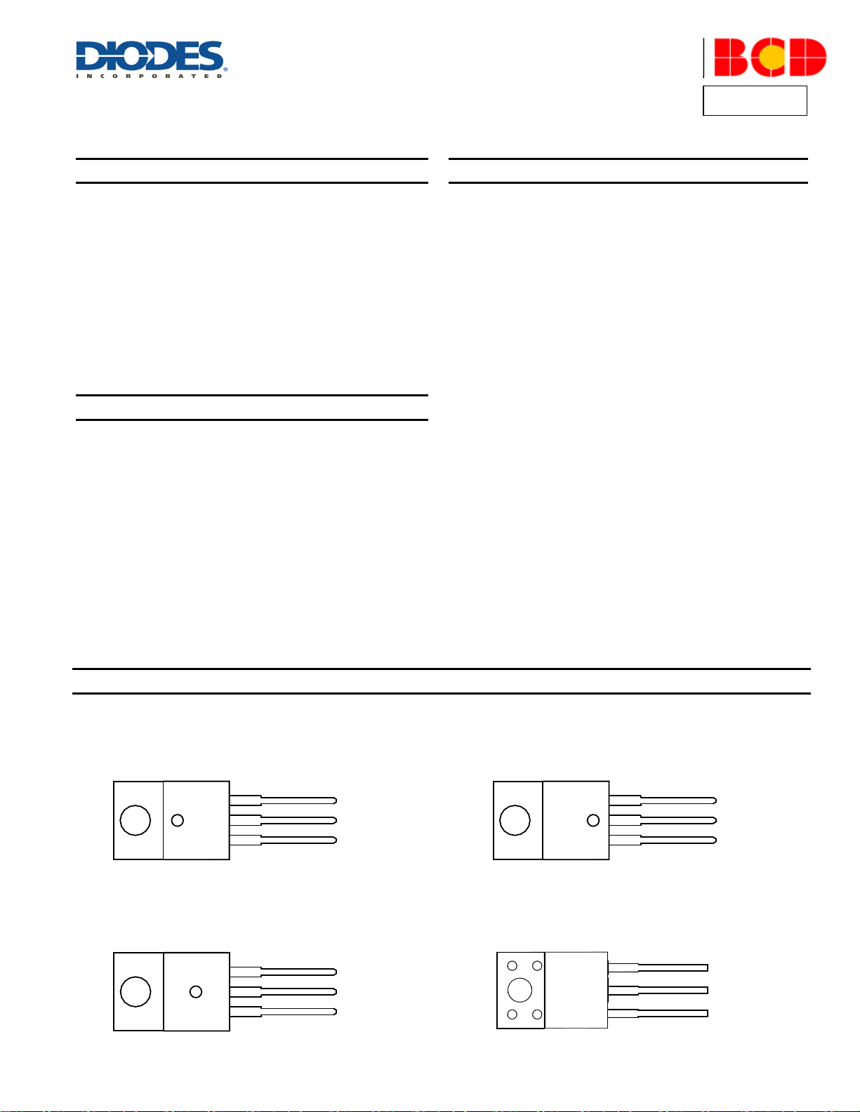
Pin Assignments
T Package T Package
(TO-220-3) (Option 1) (TO-220-3) (Option 2)
T Package TF Package
(TO-220-3) (Option 3) (TO-220F-3)
AS78XXA
Document number: DS36562 Rev. 3 - 2
3
2
1
OUTPUT
GND
INPUT
3
2
1
OUTPUT
GND
INPUT
3
2
1
OUTPUT
GND
INPUT
3
2
1
1 of 23
www.diodes.com
OUTPUT
GND
INPUT
September 2013
© Diodes Incorporated
Page 2
A
A
f
Product Line o
Diodes Incorporated
S78XXA
Pin Assignments
(TO-252-2 (3)) (Option 1) (TO-252-2 (3)) (Option 2)
(Cont.)
D Package
3
2
OUTPUT
GND
3
2
1
INPUT
1
(TO-252-2 (4)) (TO-252-2 (5))
3
OUTPUT
2
GND
1
INPUT
3
2
1
OUTPUT
GND
INPUT
OUTPUT
GND
INPUT
Typical Applications Circuit
V
IN
AS78XXA
1
INPUT OUTPUT
GND
2
Pin Descriptions
Pin Number Pin Name Function
1 INPUT Voltage Input
2 GND Ground
3 OUTPUT Voltage Output
3
V
OUT
0.1F0. 33F
AS78XXA
Document number: DS36562 Rev. 3 - 2
2 of 23
www.diodes.com
September 2013
© Diodes Incorporated
Page 3
A
A
f
Product Line o
Diodes Incorporated
S78XXA
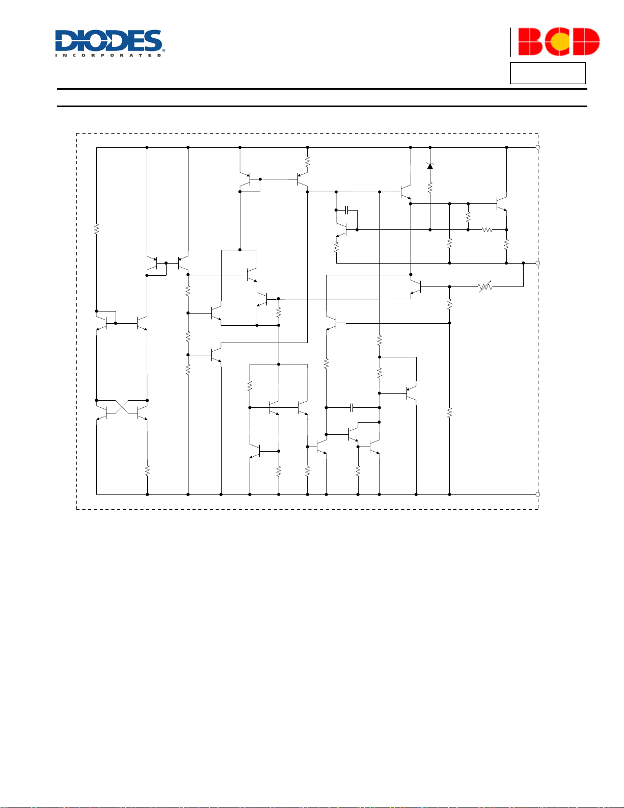
Functional Block Diagram
R1
Q3
Q1 Q4
Q2
Q5
Q6
R3
R4
R5
1
INPUT
Q8
R9
Q9
Q10
Q11
Q7
R7
R6
Q13
Q14
Q21
C1
Q18
R12
Q22
Q16
R14
R11
R15
Q15
C2
R16
Q23
D1
Zener
R17
R18
R19
R20
R21
R2
2
Q24
R23
3
OUTPU T
Q19
Q12
R2
R8 R10
Q17
R13
Q20
2
GND
AS78XXA
Document number: DS36562 Rev. 3 - 2
3 of 23
www.diodes.com
September 2013
© Diodes Incorporated
Page 4
A
A
f
Product Line o
Diodes Incorporated
S78XXA
Absolute Maximum Ratings
(Note 5)
Symbol Parameter
VIN
T
LEAD
P
D
T
J
T
STG
JA
ESD ESD (Human Body Model) 6000 V
ESD ESD (Machine Model) 500 V
Note 5: Stresses greater than those listed under “Absolute Maximum Ratings” may cause permanent damage to the device. These are stress ratings only, and
functional operation of the device at these or any other conditions beyond those indicated under “Recommended Operating Conditions” is not implied. Exposure to
“Absolute Maximum Ratings” for extended periods may affect device reliability.
Input Voltage 36 V
Lead Temperature (Soldering, 10sec) +260 °C
Power Dissipation Internally Limited W
Operating Junction Temperature +150 °C
Storage Temperature Range -65 to +150 °C
TO-220-3 60
Thermal Resistance
TO-252-2 (3)/TO-252-2
(4)/TO-252-2 (5)
TO-220F-3 60
Rating
100
Recommended Operating Conditions
Unit
°C/W
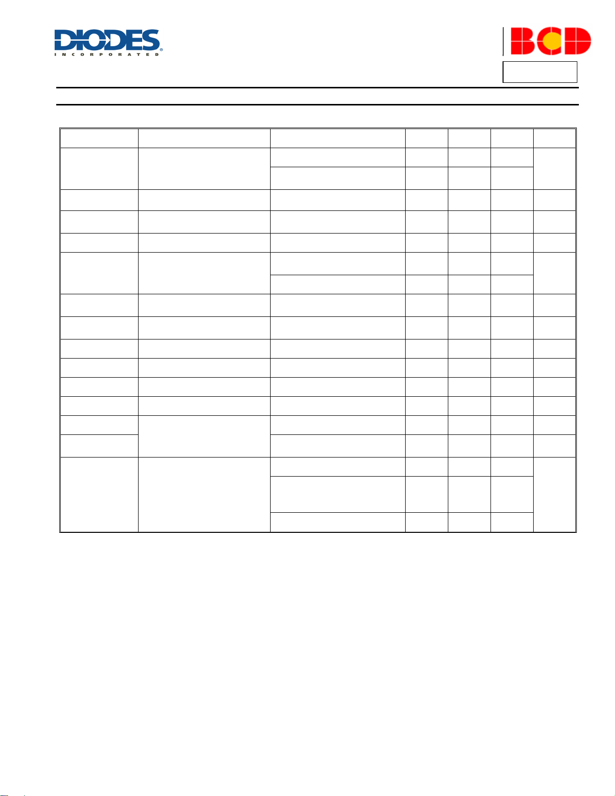
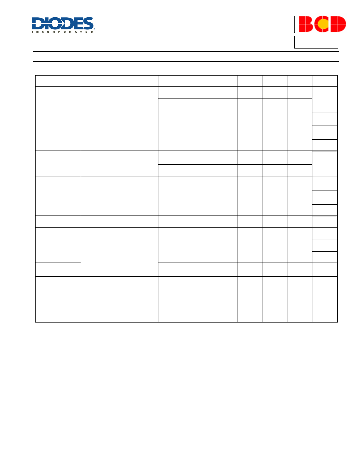
Symbol Parameter Min Max Unit
AS7805A – 25
AS7806A – 26
AS7808A – 28
VIN
T
Input Voltage
J
Operating Junction Temperature Range -40 +125 °C
AS7809A – 29
AS7812A – 32
AS7815A – 32
AS7818A – 32
V
AS78XXA
Document number: DS36562 Rev. 3 - 2
4 of 23
www.diodes.com
September 2013
© Diodes Incorporated
Page 5

A
A
f
Product Line o
Diodes Incorporated
S78XXA
Electrical Characteristics
AS7805A
(@ VIN = 10V, I
= 1A, TJ = -40 to +125°C, unless otherwise specified.)
OUT
Symbol Parameter Conditions Min Typ Max Unit
T
V
V
RLINE
V
RLOAD
△I
OUT
I
Q
Q
Output Voltage
Line Regulation
Load Regulation
Quiescent Current
Quiescent Current Change
PSRR Ripple Rejection
V
DROP
N
O
Dropout Voltage
Output Noise Voltage
= +25°C
J
I
= 5mA to 1A, VIN = 7.5V to
OUT
20V, P
≤15W
D
V
= 7.5V to 20V,
IN
= 500mA, TJ = +25°C
I
OUT
V
= 10V, I
IN
= 5mA to 1A, TJ =
OUT
+25°C
V
= 10V, I
IN
V
= 8V to 25V, I
IN
OUT
= 0
OUT
= 500mA, TJ
= +25°C
I
= 5mA to 1A, TJ = +25°C
OUT
= 8V to 18V, f = 120Hz, I
V
IN
500mA
△ V
= 1%, I
OUT
= 1A, TJ =
OUT
+25°C
f = 10Hz to 100kHz, T
= +25°C
A
OUT
4.9 5 5.1
4.8 – 5.2
–
25 50
– 20 50 mV
– 3.2 6 mA
– 0.3 0.8
– 0.08 0.5
=
– 70 – dB
– 2 – V
– 10 –
V
mV
mA
µV/V
O
△V
(△V
R
O
I
SC
IPK
/△T
OUT
OUT/VOUT
△T
Output Resistance
Short Circuit Current
Peak Output Current
Output Voltage Temperature
)/
Coefficient
f = 1kHz
= 35V, TA = +25°C
V
IN
VIN = 10V, TJ = +25°C
– 10 –
– 0.05 – A
– 2.2 – A
– – 0.4 –
– – 80 –
mΩ
mV/°C
ppm/°C
TO-220-3 – 9 –
TO-252-2 (3)/
θ
JC
Thermal Resistance
TO-252-2 (4)/
– 16 –
°C/W
TO-252-2 (5)
TO-220F-3 – 9 –
AS78XXA
Document number: DS36562 Rev. 3 - 2
5 of 23
www.diodes.com
September 2013
© Diodes Incorporated
Page 6
A
A
f
Product Line o
Diodes Incorporated
S78XXA
Electrical Characteristics
AS7806A
(@ VIN = 11V, I
OUT
(Cont.)
= 1A, TJ = -40 to +125°C, unless otherwise specified.)
Symbol Parameter Conditions Min Typ Max Unit
T
V
V
RLINE
V
RLOAD
△I
OUT
I
Q
Q
Output Voltage
Line Regulation
Load Regulation
Quiescent Current
Quiescent Current Change
PSRR Ripple Rejection
V
DROP
N
O
R
O
I
SC
Dropout Voltage
Output Noise Voltage
Output Resistance
Short Circuit Current
= +25°C
J
I
= 5mA to 1A, VIN = 8.6V to
OUT
21V, P
≤15W
D
V
= 8.6V to 21V,
IN
= 500mA, TJ = +25°C
I
OUT
V
= 11V, I
IN
= 5mA to 1A, TJ =
OUT
+25°C
V
= 11V, I
IN
V
= 8.6V to 21V, I
IN
= +25°C
T
J
I
= 5mA to 1A, TJ = +25°C
OUT
= 9.5V to 19.5V, f = 120Hz,
V
IN
I
= 500mA
OUT
△ V
OUT
= 0
OUT
= 1%, I
= 500mA,
OUT
= 1A, TJ =
OUT
+25°C
f = 10Hz to 100kHz, T
= 25°C
A
f = 1kHz
= 35V, TA = +25°C
V
IN
5.88 6 6.12
V
5.76 – 6.24
–
25 60
mV
– 20 60 mV
– 3.2 6 mA
– 0.3 0.8
mA
– 0.08 0.5
– 65 – dB
– 2 – V
– 10 –
– 10 –
µV/V
mΩ
O
– 0.2 – A
△V
(△V
IPK
/△T
OUT
OUT/VOUT
△T
Peak Output Current
Output Voltage Temperature
)/
Coefficient
VIN = 11V, TJ = +25°C
– – 0.5 –
– – 80 –
– 2.2 – A
mV/°C
ppm/°C
TO-220-3 – 9 –
TO-252-2 (3)/
θ
JC
Thermal Resistance
TO-252-2 (4)/
– 16 –
°C/W
TO-252-2 (5)
TO-220F-3 – 9 –
AS78XXA
Document number: DS36562 Rev. 3 - 2
6 of 23
www.diodes.com
September 2013
© Diodes Incorporated
Page 7
A
A
f
Product Line o
Diodes Incorporated
S78XXA
Electrical Characteristics
AS7808A
(@VIN = 14V, I
OUT
(Cont.)
= 1A, TJ = -40 to +125°C, unless otherwise specified.)
Symbol Parameter Conditions Min Typ Max Unit
= +25°C
V
V
RLINE
V
RLOAD
△I
OUT
I
Q
Q
Output Voltage
Line Regulation
Load Regulation
Quiescent Current
Quiescent Current Change
PSRR Ripple Rejection
V
DROP
N
O
R
O
Dropout Voltage
Output Noise Voltage
Output Resistance
T
J
I
= 5mA to 1A, VIN = 10.6V to
OUT
23V, P
≤15W
D
V
= 10.6V to 23V,
IN
= 500mA, TJ = +25°C
I
OUT
= 14V, I
V
IN
= 5mA to 1A, TJ =
OUT
+25°C
V
= 14V, I
IN
= 10.6V to 23V, I
V
IN
= +25°C
T
J
I
= 5mA to 1A, TJ = +25°C
OUT
V
= 11.5V to 21.5V, f = 120Hz,
IN
= 500mA
I
OUT
△ V
OUT
= 0
OUT
= 1%, I
= 500mA,
OUT
= 1A, TJ =
OUT
+25°C
f = 10Hz to 100kHz, T
= +25°C
A
f = 1kHz
7.84 8 8.16
V
7.7 – 8.3
–
–
25 75
25 75
mV
mV
– 3.2 6 mA
– 0.3 0.8
mA
– 0.08 0.5
– 62 – dB
– 2 – V
– 10 –
– 10 –
µV/V
mΩ
O
△V
(△V
I
SC
IPK
/△T
OUT
OUT/VOUT
△T
Short Circuit Current
Peak Output Current
Output Voltage Temperature
)/
Coefficient
= 35V, TA = +25°C
V
IN
VIN = 14V, TJ = +25°C
– – 0.64 –
– – 80 –
– 0.2 – A
– 2.2 – A
mV/°C
ppm/°C
TO-220-3 – 9 –
TO-252-2 (3)/
θ
JC
Thermal Resistance
TO-252-2 (4)/
– 16 –
°C/W
TO-252-2 (5)
TO-220F-3 – 9 –
AS78XXA
Document number: DS36562 Rev. 3 - 2
7 of 23
www.diodes.com
September 2013
© Diodes Incorporated
Page 8

A
A
f
Product Line o
Diodes Incorporated
S78XXA
Electrical Characteristics
AS7809A
(@ VIN = 15V, I
OUT
(Cont.)
= 1A, TJ = -40 to +125°C, unless otherwise specified.)
Symbol Parameter Conditions Min Typ Max Unit
T
V
V
RLINE
V
RLOAD
△I
OUT
I
Q
Q
Output Voltage
Line Regulation
Load Regulation
Quiescent Current
Quiescent Current Change
PSRR Ripple Rejection
V
DROP
N
O
R
O
I
SC
Dropout Voltage
Output Noise Voltage
Output Resistance
Short Circuit Current
= +25°C
J
I
= 5mA to 1A, VIN = 11.5V to
OUT
23V, P
≤15W
D
V
= 11.5V to 23V,
IN
= 500mA, TJ = +25°C
I
OUT
V
= 14V, I
IN
= 5mA to 1A, TJ =
OUT
+25°C
V
= 15V, I
IN
V
= 11.5V to 23V, I
IN
= +25°C
T
J
I
= 5mA to 1A, TJ = +25°C
OUT
= 11.5V to 21.5V, f = 120Hz,
V
IN
I
= 500mA
OUT
△ V
OUT
= 0
OUT
= 1%, I
= 500mA,
OUT
= 1A, TJ =
OUT
+25°C
f = 10Hz to 100kHz, T
= +25°C
A
f = 1kHz
= 35V, TA = +25°C
V
IN
8.82 9 9.18
V
8.65 – 9.35
–
–
25 90
25 100
mV
mV
– 3.2 6 mA
– 0.3 0.8
mA
– 0.08 0.5
– 61 – dB
– 2 – V
– 10 –
– 10 –
µV/V
mΩ
O
– 0.2 – A
△V
(△V
IPK
/△T
OUT
OUT/VOUT
△T
Peak Output Current
Output Voltage Temperature
)/
Coefficient
VIN = 15V, TJ = +25°C
– – 0.72 –
– – 80 –
– 2.2 – A
mV/°C
ppm/°C
TO-220-3 – 9 –
TO-252-2 (3)/
θ
JC
Thermal Resistance
TO-252-2 (4)/
– 16 –
°C/W
TO-252-2 (5)
TO-220F-3 – 9 –
AS78XXA
Document number: DS36562 Rev. 3 - 2
8 of 23
www.diodes.com
September 2013
© Diodes Incorporated
Page 9

A
A
f
Product Line o
Diodes Incorporated
S78XXA
Electrical Characteristics
AS7812A
(@ VIN = 19V, I
OUT
(Cont.)
= 1A, TJ = -40 to +125°C, unless otherwise specified.)
Symbol Parameter Conditions Min Typ Max Unit
T
V
V
RLINE
V
RLOAD
△I
OUT
I
Q
Q
Output Voltage
Line Regulation
Load Regulation
Quiescent Current
Quiescent Current Change
PSRR Ripple Rejection
V
DROP
N
O
R
O
I
SC
Dropout Voltage
Output Noise Voltage
Output Resistance
Short Circuit Current
= +25°C
J
I
= 5mA to 1A, VIN = 14.8V to
OUT
27V, P
≤15W
D
V
= 14.8V to 27V,
IN
= 500mA, TJ = +25°C
I
OUT
V
= 19V, I
IN
= 5mA to 1A, TJ =
OUT
25°C
V
= 19V, I
IN
V
= 14.8V to 30V, I
IN
= 25°C
T
J
I
= 5mA to 1A, TJ = +25°C
OUT
= 15V to 25V, f = 120Hz, I
V
IN
OUT
= 0
= 500mA,
OUT
= 500mA
△ V
= 1%, I
OUT
= 1A, TJ =
OUT
+25°C
f = 10Hz to 100kHz, T
= +25°C
A
f = 1kHz
= 35V, TA = +25°C
V
IN
11.75 12 12.25
11.5 – 12.5
–
–
25 120
40 120
– 3.4 6 mA
– 0.3 0.8
– 0.08 0.5
OUT
– 60 – dB
– 2 – V
– 10 –
– 11 –
– 0.2 – A
V
mV
mV
mA
µV/V
mΩ
O
△V
(△V
IPK
/△T
OUT
OUT/VOUT
△T
θ
JC
Peak Output Current
Output Voltage Temperature
)/
Coefficient
Thermal Resistance
VIN = 18V, TJ = +25°C
– – 0.96 –
– – 80 –
– 2.2 – A
mV/°C
ppm/°C
TO-220-3 – 9 –
TO-252-2 (3)/
TO-252-2 (4)/
– 16 –
°C/W
TO-252-2 (5)
TO-220F-3 – 9 –
AS78XXA
Document number: DS36562 Rev. 3 - 2
9 of 23
www.diodes.com
September 2013
© Diodes Incorporated
Page 10

A
A
f
Product Line o
Diodes Incorporated
S78XXA
Electrical Characteristics
AS7815A
(@ VIN = 23V, I
OUT
(Cont.)
= 1A, TJ = -40 to +125°C, unless otherwise specified.)
Symbol Parameter Conditions Min Typ Max Unit
T
V
V
RLINE
V
RLOAD
△I
OUT
I
Q
Q
Output Voltage
Line Regulation
Load Regulation
Quiescent Current
Quiescent Current Change
PSRR Ripple Rejection
V
DROP
N
O
R
O
I
SC
Dropout Voltage
Output Noise Voltage
Output Resistance
Short Circuit Current
= +25°C
J
I
= 5mA to 1A, VIN = 17.9V to
OUT
30V, P
≤15W
D
V
= 17.9V to 30V,
IN
= 500mA, TJ = +25°C
I
OUT
V
= 23V, I
IN
= 5mA to 1A, TJ =
OUT
+25°C
V
= 23V, I
IN
V
= 17.9V to 30V, I
IN
= +25°C
T
J
I
= 5mA to 1A, TJ = +25°C
OUT
= 18.5V to 28.5V, f = 120Hz,
V
IN
I
= 500mA
OUT
△ V
OUT
= 0
OUT
= 1%, I
= 500mA,
OUT
= 1A, TJ =
OUT
+25°C
f = 10Hz to 100kHz, T
= +25°C
A
f = 1kHz
= 35V, TA = +25°C
V
IN
14.7 15 15.3
V
14.4 – 15.6
–
–
35 150
70 150
mV
mV
– 3.4 6 mA
– 0.3 0.8
mA
– 0.08 0.5
– 58 – dB
– 2 – V
– 10 –
– 11 –
µV/V
mΩ
O
– 0.2 – A
△V
(△V
IPK
/△T
OUT
OUT/VOUT
△T
θ
JC
Peak Output Current
Output Voltage Temperature
)/
Coefficient
Thermal Resistance
VIN = 21V, TJ = +25°C
– – 1.2 –
– – 80 –
– 2.2 – A
mV/°C
ppm/°C
TO-220-3 – 9 –
TO-252-2 (3)/
TO-252-2 (4)/
– 16 –
°C/W
TO-252-2 (5)
TO-220F-3 – 9 –
AS78XXA
Document number: DS36562 Rev. 3 - 2
10 of 23
www.diodes.com
September 2013
© Diodes Incorporated
Page 11

A
A
f
Product Line o
Diodes Incorporated
S78XXA
Electrical Characteristics
AS7818A
(@ VIN = 27V, I
OUT
(Cont.)
= 1A, TJ = -40 to +125°C, unless otherwise specified.)
Symbol Parameter Conditions Min Typ Max Unit
T
V
V
RLINE
V
RLOAD
△I
OUT
I
Q
Q
Output Voltage
Line Regulation
Load Regulation
Quiescent Current
Quiescent Current Change
PSRR Ripple Rejection
V
DROP
N
O
R
O
I
SC
Dropout Voltage
Output Noise Voltage
Output Resistance
Short Circuit Current
= +25°C
J
I
= 5mA to 1A, VIN = 21V to
OUT
33V, P
≤15W
D
V
= 21V to 33V,
IN
= 500mA, TJ = +25°C
I
OUT
V
= 27V, I
IN
= 5mA to 1A, TJ =
OUT
+25°C
V
= 27V, I
IN
V
= 21V to 33V, I
IN
= +25°C
T
J
I
= 5mA to 1A, TJ = +25°C
OUT
= 22V to 32V, f = 120Hz, I
V
IN
OUT
= 0
= 500mA,
OUT
= 500mA
△ V
= 1%, I
OUT
= 1A, TJ =
OUT
+25°C
f = 10Hz to 100kHz, T
= +25°C
A
f = 1kHz
= 35V, TA = +25°C
V
IN
17.64 18 18.36
17.3 – 18.7
–
–
45 180
85 180
– 3.6 6 mA
– 0.3 0.8
– 0.08 0.5
OUT
– 57 – dB
– 2 – V
– 10 –
– 11 –
– 0.2 – A
V
mV
mV
mA
µV/V
mΩ
O
(△V
IPK
△V
OUT
OUT/VOUT
△T
θ
JC
/△T
Peak Output Current
Output Voltage Temperature
)/
Coefficient
Thermal Resistance
VIN = 24V, TJ = +25°C
– – 1.44 –
– – 80 –
– 2.2 – A
mV/°C
ppm/°C
TO-220-3 – 9 –
TO-252-2 (3)/
TO-252-2 (4)/
– 16 –
°C/W
TO-252-2 (5)
TO-220F-3 – 9 –
AS78XXA
Document number: DS36562 Rev. 3 - 2
11 of 23
www.diodes.com
September 2013
© Diodes Incorporated
Page 12

A
A
f
Product Line o
Diodes Incorporated
S78XXA
Performance Characteristics
Peak Output Current vs. Input/Output Differential Voltage Output Voltage vs. Junction Temperature
2.5
2.0
1.5
Peak Output Current (A)
1.0
0.5
0.0
3 6 9 12 15 18 21 24
VIN-V
AS7805A
(V)
OUT
TJ=-40OC
TJ=25OC
TJ=125OC
5.050
5.025
5.000
4.975
4.950
4.925
Output Voltage (V)
4.900
4.875
4.850
-40 -20 0 20 40 60 80 100 120
Junction Temperature (OC)
AS7805A
=10V
V
IN
I
OUT
I
OUT
Output Voltage vs. Output Current Output Voltage vs. Input Voltage
5.050
5.025
5.000
4.975
4.950
4.925
Output Voltage (V)
4.900
4.875
4.850
0 200 400 600 800 1000 1200 1400
Output Current (mA)
AS7805A
=10V, TJ=25OC
V
IN
5.050
5.025
5.000
4.975
4.950
4.925
Output Voltage (V)
4.900
4.875
4.850
8 1012141618202224
AS7805A
Input Voltage (V)
I
=500mA, TJ=25OC
OUT
I
=500mA, TJ=75OC
OUT
I
=1A, TJ=25OC
OUT
Quiescent Current vs. Junction Temperature Ripple Rejection vs. Frequency
6
100
5
4
3
2
Quiescent Current (mA)
1
AS7805A
=10V, I
V
IN
=0
OUT
80
60
40
Ripple Rejection (dB)
20
AS7805A
=10mA
=1A
0
-40 -20 0 20 40 60 80 100 120
Junction Temperature (OC)
AS78XXA
Document number: DS36562 Rev. 3 - 2
0
10 100 1k 10k 100k 1M
Frequency (Hz)
12 of 23
www.diodes.com
September 2013
© Diodes Incorporated
Page 13

A
A
f
Product Line o
Diodes Incorporated
S78XXA
Performance Characteristics
Dropout Voltage vs. Junction Temperature Power Dissipation vs. Junction Temperature
2.5
2.0
1.5
1.0
Dropout Voltage (V)
AS7805A
I
=100mA
OUT
I
0.5
0.0
-40 -20 0 20 40 60 80 100 120
=500mA
OUT
I
=1A
OUT
Junction Temperature (OC)
(Conditions: I
25
20
15
(5V/D iv)
IN
V
10
0
(50 mV /Div )
V
-100
OUT
-150
-50
Line Transient Load Transient
= 500mA, C
OUT
Time (100µs/Div)
(Cont.)
30
25
20
= 0.1µF) (Conditions: VIN = 10V, CIN = 0.33µF, C
OUT
AS7805A
15
10
Power Dissipation (W )
5
0
-40-20 0 20406080100120
Junction Temperature (OC)
2
1
0
(1A /Div )
0 .0 05A
Time (40µs/Div)
(1 0 0 m V /D i v )
V
I
OUT
OUT
-1
100
0
-10 0
-20 0
AS7805A
Package: TO-220-3
Heatsink: 60*43mm
AS 78 05A
= 0.1µF)
OUT
2
AS78XXA
Document number: DS36562 Rev. 3 - 2
13 of 23
www.diodes.com
September 2013
© Diodes Incorporated
Page 14

A
A
f
Ordering Information
Circuit Type
Output Voltage
05: 5V
06: 6V
08: 8V
09: 9V
12: 12V
15: 15V
18: 18V
Product Line o
Diodes Incorporated
S78XXA
AS78XXA
-
E1: Lead Free
G1: Green
TR: Tape & Reel
Blank: Tube
Package
T: TO-220-3
TF: TO-220F-3
D: TO-252-2 (3)/
TO-252-2 (4)/
TO-252-2 (5)
Pb
Green
Pb
Green
Pb
Lead-Fr ee
Package
TO-220-3 -40 to +125C
TO-220F-3 -40 to +125C
TO-252-2 (3)/
TO-252-2 (4)/
TO-252-2 (5)
Temperature
-40 to +125C
Range
Lead Free Green Lead Free Green
AS7805AT-E1 AS7805AT-G1 AS7805AT-E1 AS7805AT-G1
AS7806AT-E1 AS7806AT-G1 AS7806AT-E1 AS7806AT-G1
AS7808AT-E1 AS7808AT-G1 AS7808AT-E1 AS7808AT-G1
AS7809AT-E1 AS7809AT-G1 AS7809AT-E1 AS7809AT-G1
AS7812AT-E1 AS7812AT-G1 AS7812AT-E1 AS7812AT-G1
AS7815AT-E1 AS7815AT-G1 AS7815AT-E1 AS7815AT-G1
AS7818AT-E1 AS7818AT-G1 AS7818AT-E1 AS7818AT-G1
AS7805ATF-E1 AS7805ATF-G1 AS7805ATF-E1 AS7805ATF-G1
AS7806ATF-E1 AS7806ATF-G1 AS7806ATF-E1 AS7806ATF-G1
AS7808ATF-E1 AS7808ATF-G1 AS7808ATF-E1 AS7808ATF-G1
AS7809ATF-E1 AS7809ATF-G1 AS7809ATF-E1 AS7809ATF-G1
AS7812ATF-E1 AS7812ATF-G1 AS7812ATF-E1 AS7812ATF-G1
AS7815ATF-E1 AS7815ATF-G1 AS7815ATF-E1 AS7815ATF-G1
AS7818ATF-E1 AS7818ATF-G1 AS7818ATF-E1 AS7818ATF-G1
AS7805ADTR-E1 AS7805ADTR-G1 AS7805AD-E1 AS7805AD-G1
AS7806ADTR-E1 AS7806ADTR-G1 AS7806AD-E1 AS7806AD-G1
AS7808ADTR-E1 AS7808ADTR-G1 AS7808AD-E1 AS7808AD-G1
AS7809ADTR-E1 AS7809ADTR-G1 AS7809AD-E1 AS7809AD-G1
AS7812ADTR-E1 AS7812ADTR-G1 AS7812AD-E1 AS7812AD-G1
AS7815ADTR-E1 AS7815ADTR-G1 AS7815AD-E1 AS7815AD-G1
AS7818ADTR-E1 AS7818ADTR-G1 AS7818AD-E1 AS7818AD-G1
Part Number Marking ID
Packing
Type
Tube
Tube
Tube
Tube
Tube
Tube
Tube
Tube
Tube
Tube
Tube
Tube
Tube
Tube
Tape &
Reel
Tape &
Reel
Tape &
Reel
Tape &
Reel
Tape &
Reel
Tape &
Reel
Tape &
Reel
BCD Semiconductor's Pb-free products, as designated with "E1" suffix in the part number, are RoHS compliant. Products with "G1" suffix are available in green
packages.
AS78XXA
Document number: DS36562 Rev. 3 - 2
14 of 23
www.diodes.com
September 2013
© Diodes Incorporated
Page 15

A
A
f
Product Line o
Diodes Incorporated
S78XXA
Package Outline Dimensions
9.660(0.380)
10.660(0. 420)
Option 1
φ1.500(0.059)
1.150(0. 045)
1.770(0. 070)
(All dimensions in mm(inch).)
TO-220-3
0
2
.
(
4
5
0
0
3
.
(
2
4
φ
3.540(0. 139)
4.080(0.161)
0
)
)
0
5
3
7
3
3
.
.
0
0
(
(
)
0
0
8
9
2
9
3
5
.
.
0
.
8
9
1
(
0
8
8
.
7
2
.
)
1
0
0
.
)
1
3
5
)
)
0
0
6
5
5
6
.
.
0
0
(
(
0
0
2
1
2
5
.
.
4
6
1
)
2
9
1
.
1
(
0
8
2
.
0
3
1
3
°
0.510(0.020)
1.390(0.055)
0.200(0. 008)
3.560(0.140)
4.820(0.190)
7
°
2.040(0.080)
2.920(0.115)
°
7
0.813(0. 032)
0.381(0.015)
2.540(0. 100)
Option 2
2.540( 0.100)
Option 3
0.356 (0.014)
0.610(0. 024)
AS78XXA
Document number: DS36562 Rev. 3 - 2
15 of 23
www.diodes.com
September 2013
© Diodes Incorporated
Page 16

A
A
f
Product Line o
Diodes Incorporated
S78XXA
Package Outline Dimensions
3.000(0.119)
3. 550( 0. 140)
14. 700(0.579)
16. 000(0.630)
(Cont. All dimensions in mm(inch).)
TO-220F-3
9.700(0.382)
10.300(0. 406)
6. 900(0. 272)
7.10 0(0. 280)
3.000(0.119)
3.400(0.134)
3.370(0.133)
3.900(0.154)
Option 1
2.350( 0. 093)
2.900( 0. 114)
4.300(0.169)
4.900(0.193)
12. 500(0.492)
13. 500(0.531)
2.790(0.110)
4.500(0.177)
0.500(0.020)
0.900(0.035)
2. 540( 0.10 0)
1. 00 0(0.039)
1. 40 0(0.055)
1.100( 0. 043)
1.500( 0. 059)
2. 54 0(0.100)
2.520(0.099)
2.920(0.115)
Option 2
5 5
0.450(0.018)
0.650(0.026)
3. 19 0( 0 . 1 2 6)
3. 25 0( 0 . 1 2 8)
5
AS78XXA
Document number: DS36562 Rev. 3 - 2
16 of 23
www.diodes.com
September 2013
© Diodes Incorporated
Page 17

A
A
f
Product Line o
Diodes Incorporated
S78XXA
Package Outline Dimensions
6. 5 00( 0 . 25 6)
6. 7 00( 0 . 26 4)
5.130(0.202)
0. 900( 0. 03 5)
1.250(0.049)
5.460(0.215)
6.000(0.236)
6.200(0.244)
1.800REF
0.720(0.028)
0.900(0.035)
2.286(0.090)
BSC
5
9
0.150(0.006)
0.720(0.028)
0.850(0.033)
(Cont. All dimensions in mm(inch).)
TO-252-2 (3)
1.29±0.1
Option 1
0.750(0.030)
2. 200( 0. 08 7)
2.380(0.094)
4.700REF
0.600(0.024)
1.000(0.039)
0.470(0. 019)
0.600(0.024)
5
9
0
8
0.900(0.035)
1.100(0.043)
3
7
5.250REF
0
8
9.800(0.386)
10.400(0.409)
2.900R EF
)
7
.700(0.06
1. 400( 0. 05 5)1
Option 2
AS78XXA
Document number: DS36562 Rev. 3 - 2
17 of 23
www.diodes.com
September 2013
© Diodes Incorporated
Page 18

A
A
f
Product Line o
Diodes Incorporated
S78XXA
Package Outline Dimensions
(Cont. All dimensions in mm(inch).)
TO-252-2 (4)
AS78XXA
Document number: DS36562 Rev. 3 - 2
18 of 23
www.diodes.com
September 2013
© Diodes Incorporated
Page 19

A
A
f
Product Line o
Diodes Incorporated
S78XXA
Package Outline Dimensions
(Cont. All dimensions in mm(inch).)
TO-252-2 (5)
AS78XXA
Document number: DS36562 Rev. 3 - 2
19 of 23
www.diodes.com
September 2013
© Diodes Incorporated
Page 20

A
A
f
Product Line o
Diodes Incorporated
S78XXA
Suggested Pad Layout
TO-252-2 (3)
X2
Y2
Z
Dimensions
Value 11.600/0.457 1.500/0.059 7.000/0.276 2.500/0.098 2.100/0.083 2.300/0.091
(mm)/(inch)
AS78XXA
Document number: DS36562 Rev. 3 - 2
G
Y1
E1X1
Z
X1
(mm)/(inch)
X2 = Y2
(mm)/(inch)
20 of 23
www.diodes.com
Y1
(mm)/(inch)
G
(mm)/(inch)
E1
(mm)/(inch)
September 2013
© Diodes Incorporated
Page 21

A
A
f
Product Line o
Diodes Incorporated
S78XXA
Suggested Pad Layout
Z
(Cont.)
TO-252-2 (4)
X2
Y2
Dimensions
Value 11.600/0.457 1.500/0.059 7.000/0.276 2.500/0.098 2.100/0.083 2.300/0.091
(mm)/(inch)
AS78XXA
Document number: DS36562 Rev. 3 - 2
G
Y1
E1X1
Z
X1
(mm)/(inch)
X2 = Y2
(mm)/(inch)
21 of 23
www.diodes.com
Y1
(mm)/(inch)
G
(mm)/(inch)
E1
(mm)/(inch)
September 2013
© Diodes Incorporated
Page 22

A
A
f
Product Line o
Diodes Incorporated
S78XXA
Suggested Pad Layout
Z
(Cont.)
TO-252-2 (5)
X2
Y2
Dimensions
Value 11.600/0.457 1.500/0.059 7.000/0.276 2.500/0.098 2.100/0.083 2.300/0.091
(mm)/(inch)
AS78XXA
Document number: DS36562 Rev. 3 - 2
G
Y1
E1X1
Z
X1
(mm)/(inch)
X2 = Y2
(mm)/(inch)
22 of 23
www.diodes.com
Y1
(mm)/(inch)
G
(mm)/(inch)
E1
(mm)/(inch)
September 2013
© Diodes Incorporated
Page 23

A
A
f
Product Line o
Diodes Incorporated
S78XXA
DIODES INCORPORATED MAKES NO WARRANTY OF ANY KIND, EXPRESS OR IMPLIED, WITH REGARDS TO THIS DOCUMENT,
INCLUDING, BUT NOT LIMITED TO, THE IMPLIED WARRANTIES OF MERCHANTABILITY AND FITNESS FOR A PARTICULAR PURPOSE
(AND THEIR EQUIVALENTS UNDER THE LAWS OF ANY JURISDICTION).
Diodes Incorporated and its subsidiaries reserve the right to make modifications, enhancements, improvements, corrections or other changes
without further notice to this document and any product described herein. Diodes Incorporated does not assume any liability arising out of the
application or use of this document or any product described herein; neither does Diodes Incorporated convey any license under its patent or
trademark rights, nor the rights of others. Any Customer or user of this document or products described herein in such applications shall assume
all risks of such use and will agree to hold Diodes Incorporated and all the companies whose products are represented on Diodes Incorporated
website, harmless against all damages.
Diodes Incorporated does not warrant or accept any liability whatsoever in respect of any products purchased through unauthorized sales channel.
Should Customers purchase or use Diodes Incorporated products for any unintended or unauthorized application, Customers shall indemnify and
hold Diodes Incorporated and its representatives harmless against all claims, damages, expenses, and attorney fees arising out of, directly or
indirectly, any claim of personal injury or death associated with such unintended or unauthorized application.
Products described herein may be covered by one or more United States, international or foreign patents pending. Product names and markings
noted herein may also be covered by one or more United States, international or foreign trademarks.
This document is written in English but may be translated into multiple languages for reference. Only the English version of this document is the
final and determinative format released by Diodes Incorporated.
Diodes Incorporated products are specifically not authorized for use as critical components in life support devices or systems without the express
written approval of the Chief Executive Officer of Diodes Incorporated. As used herein:
A. Life support devices or systems are devices or systems which:
1. are intended to implant into the body, or
2. support or sustain life and whose failure to perform when properly used in accordance with instructions for use provided in the
labeling can be reasonably expected to result in significant injury to the user.
B. A critical component is any component in a life support device or system whose failure to perform can be reasonably expected to cause the
failure of the life support device or to affect its safety or effectiveness.
Customers represent that they have all necessary expertise in the safety and regulatory ramifications of their life support devices or systems, and
acknowledge and agree that they are solely responsible for all legal, regulatory and safety-related requirements concerning their products and any
use of Diodes Incorporated products in such safety-critical, life support devices or systems, notwithstanding any devices- or systems-related
information or support that may be provided by Diodes Incorporated. Further, Customers must fully indemnify Diodes Incorporated and its
representatives against any damages arising out of the use of Diodes Incorporated products in such safety-critical, life support devices or systems.
Copyright © 2013, Diodes Incorporated
www.diodes.com
IMPORTANT NOTICE
LIFE SUPPORT
AS78XXA
Document number: DS36562 Rev. 3 - 2
23 of 23
www.diodes.com
September 2013
© Diodes Incorporated
 Loading...