

Page 1
Data Sheet
LOW POWER LOW OFFSET VOLTAGE DUAL COMPARATORS AS393/393A
General Description
The AS393/393A consist of two independent precision
voltage comparators with a typical offset voltage of
1.0mV and high gain. They are specifically designed to
operate from a single power supply over wide range of
voltages. Operation from split power supply is also
possible and the low power supply current drain is
independent of the magnitude of the power supply
voltage.
The AS393/393A series are compatible with industry
standard 393. AS393A has more stringent input offset
voltage than AS393.
The AS393 is available in standard DIP-8, TDIP-8,
SOIC-8, TSSOP-8 and MSOP-8 packages, AS393A is
available in standard DIP-8 and SOIC-8 packages.
Features
· Wide Supply Voltage Range
- Single Supply: 2.0V to 36V
- Dual Supplies: ±1.0V to ±18V
· Low Supply Current Drain: 0.6mA
· Low Input Bias Current: 25nA (Typical)
· Low Input Offset Current: ±5.0nA (Typical)
· Low Input Offset Voltage: 1.0mV (Typical)
· Input Common Mode Voltage Range Includes
Ground
· Differential Input Voltage Range Equals to the
Power Supply Voltage
· Low Output Saturation Voltage: 200mV at 4mA
· Open Collector Output
Applications
· Battery Charger
· Cordless Telephone
· Switching Power Supply
· DC-DC Module
· PC Motherboard
· Communication Equipment
Jan. 2013 Rev. 2. 3
SOIC-8
DIP-8
TSSOP-8
Figure 1. Package Types of AS393/393A
MSOP-8
BCD Semiconductor Manufacturing Limited
1
TDIP-8
Page 2
Data Sheet
+INPUT
-INPUT
Q5
Q6
Q1
Q2 Q3
Q4
Q7
Q8
OUTPUT
V
CC
1
2
3
4
8
7
6
5
1
2
3
4
8
7
6
5
LOW POWER LOW OFFSET VOLTAGE DUAL COMPARATORS AS393/393A
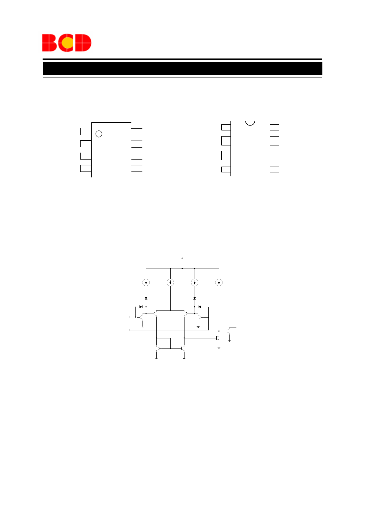
Pin Configuration
M/G/MM Package
(SOIC-8/TSSOP-8/MSOP-8)
OUTPUT1
INPUT1-
INPUT1+
GND
Figure 2. Pin Configuration of AS393/393A (Top View)
Functional Block Diagram
V
CC
OUTPUT 2
INPUT 2-
INPUT 2+
(DIP-8/TDIP-8)
OUTPUT1
INPUT1-
INPUT1+
GND
P/PT Package
V
CC
OUTPUT 2
INPUT 2-
INPUT 2+
Jan. 2013 Rev. 2. 3
Figure 3. Functional Block Diagram of AS393
/393A (Each comparator)
BCD Semiconductor Manufacturing Limited
2
Page 3
Data Sheet
LOW POWER LOW OFFSET VOLTAGE DUAL COMPARATORS AS393/393A
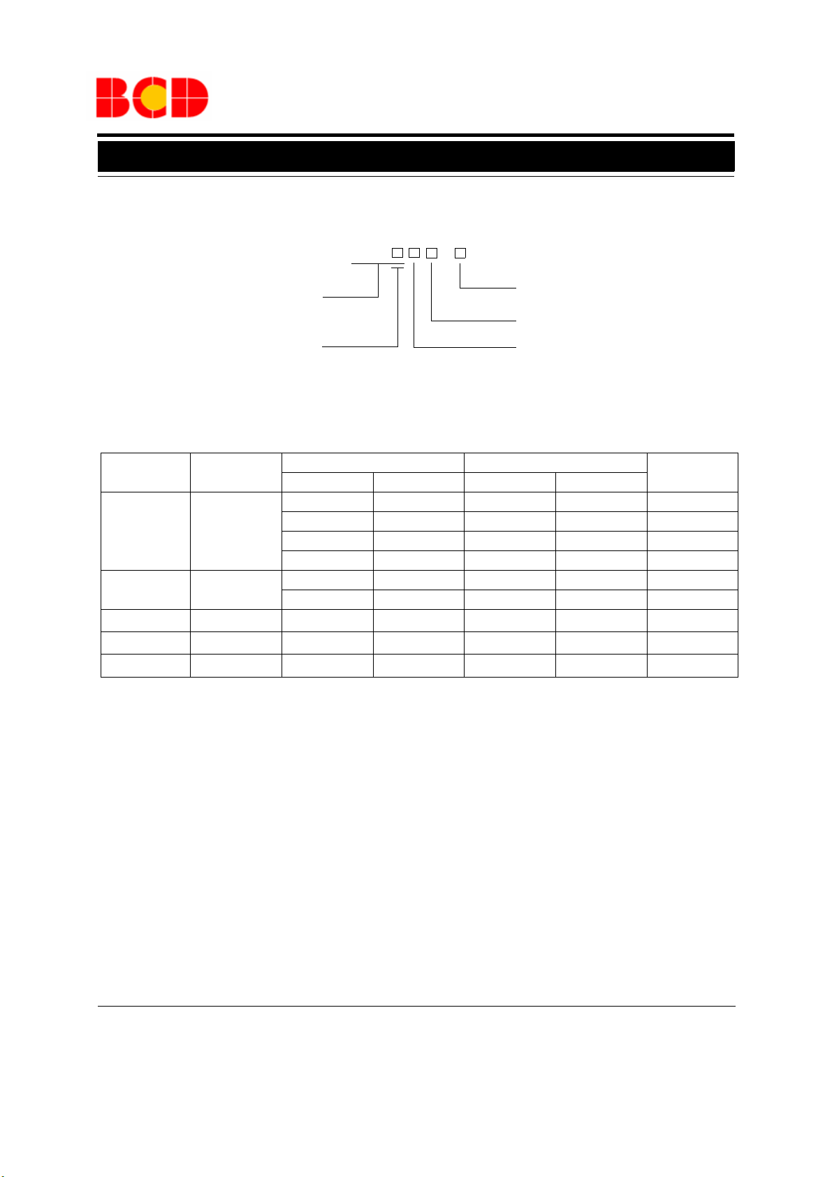
Ordering Information
Package
SOIC-8
DIP-8
TDIP-8
TSSOP-8
MSOP-8
Circuit Type
Blank: AS393
A: AS393A
Te mp er at ur e
Range
o
-40 to 85
-40 to 85
-40 to 85
-40 to 85
-40 to 85
C
o
C
o
C
o
C
o
C
AS393
-
E1: Lead Free
G1: Green
TR: Tape and Reel
Blank: Tube
Package
M: SOIC-8
P: DIP-8
PT: TDIP-8
G: TSSOP-8
MM: MSOP-8
Part Number Marking ID
Lead Free Green Lead Free Green
AS393M-E1 AS393M-G1 AS393M-E1 AS393M-G1 Tube
AS393MTR-E1 AS393MTR-G1 AS393M-E1 AS393M-G1 Tape & Reel
AS393AM-E1 AS393AM-G1 AS393AM-E1 AS393AM-G1 Tube
AS393AMTR-E1 AS393AMTR-G1 AS393AM-E1 AS393AM-G1 Tape & Reel
AS393P-E1 AS393P-G1 AS393P-E1 AS393P-G1 Tube
AS393AP-E1 AS393AP-G1 AS393AP-E1 AS393AP-G1 Tube
AS393PT-G1 AS393PT-G1 Tube
AS393GTR-E1 AS393GTR-G1 EG3C GG3C Tape & Reel
AS393MMTR-G1 AS393MM-G1 Tape & Reel
Packing Type
BCD Semiconductor's Pb-free products, as designated with "E1" suffix in the part number, are RoHS compliant. Products with
"G1" suffix are available in green packages.
Jan. 2013 Rev. 2. 3
BCD Semiconductor Manufacturing Limited
3
Page 4
Data Sheet
LOW POWER LOW OFFSET VOLTAGE DUAL COMPARATORS AS393/393A
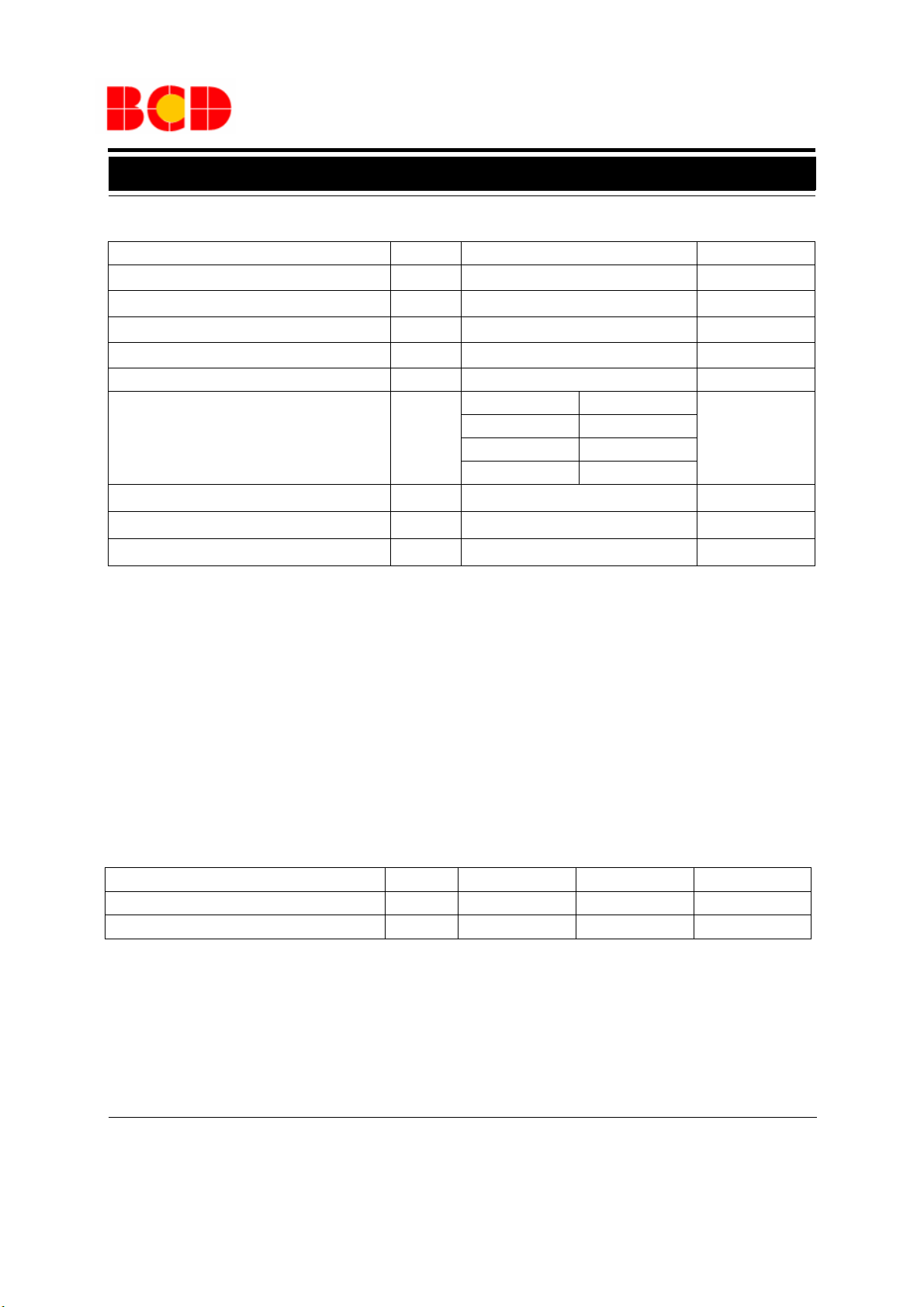
Absolute Maximum Ratings (Note 1)
Parameter Symbol Value Unit
Supply Voltage
Differential Input Voltage
Input Voltage
Input Current (V
Output Short-Circuit Current to Ground Continuous
Power Dissipation (T
Operating Junction Temperature
Storage Temperature
Lead Temperature (Soldering, 10 sec)
< -0.3V) (Note 2) I
IN
=25oC)
A
V
V
V
T
T
LEAD
CC
ID
IN
IN
P
D
T
STG
-0.3 to 40 V
DIP-8 780
SOIC-8 660
TSSOP-8 570
MSOP-8 450
J
-65 to 150
40 V
40 V
50 mA
mW
150
260
o
C
o
C
o
C
Note 1: Stresses greater than those listed under "Absolute Maximum Ratings" may cause permanent damage to the
device. These are stress ratings only, and functional operation of the device at these or any other conditions
beyond those indicated under "Recommended Operating Conditions" is not implied. Exposure to "Absolute Maximum Ratings" for extended periods may affect device reliability.
Note 2: This input current will only exist when the voltage at any of the input leads is driven negative. It is due to
the collector-base junction of the input PNP transistors becoming forward biased and thereby acting as input diode
clamps. In addition to this diode action, there is also lateral NPN parasitic transistor action on the IC chip. This
transistor action can cause the output voltages of the comparators to go to the V+ voltage level (or to ground for a
large overdrive) for the time duration that an input is driven negative. This is not destructive and normal output
states will re-establish when the input voltage, which was negative, again returns to a value greater than -0.3 V
DC
(at 25oC).
Recommended Operating Conditions
Parameter Symbol Min Max Unit
Supply Voltage V
Operating Temperature Range T
CC
A
236V
-40 85
o
C
Jan. 2013 Rev. 2. 3
BCD Semiconductor Manufacturing Limited
4
Page 5
Data Sheet
LOW POWER LOW OFFSET VOLTAGE DUAL COMPARATORS AS393/393A
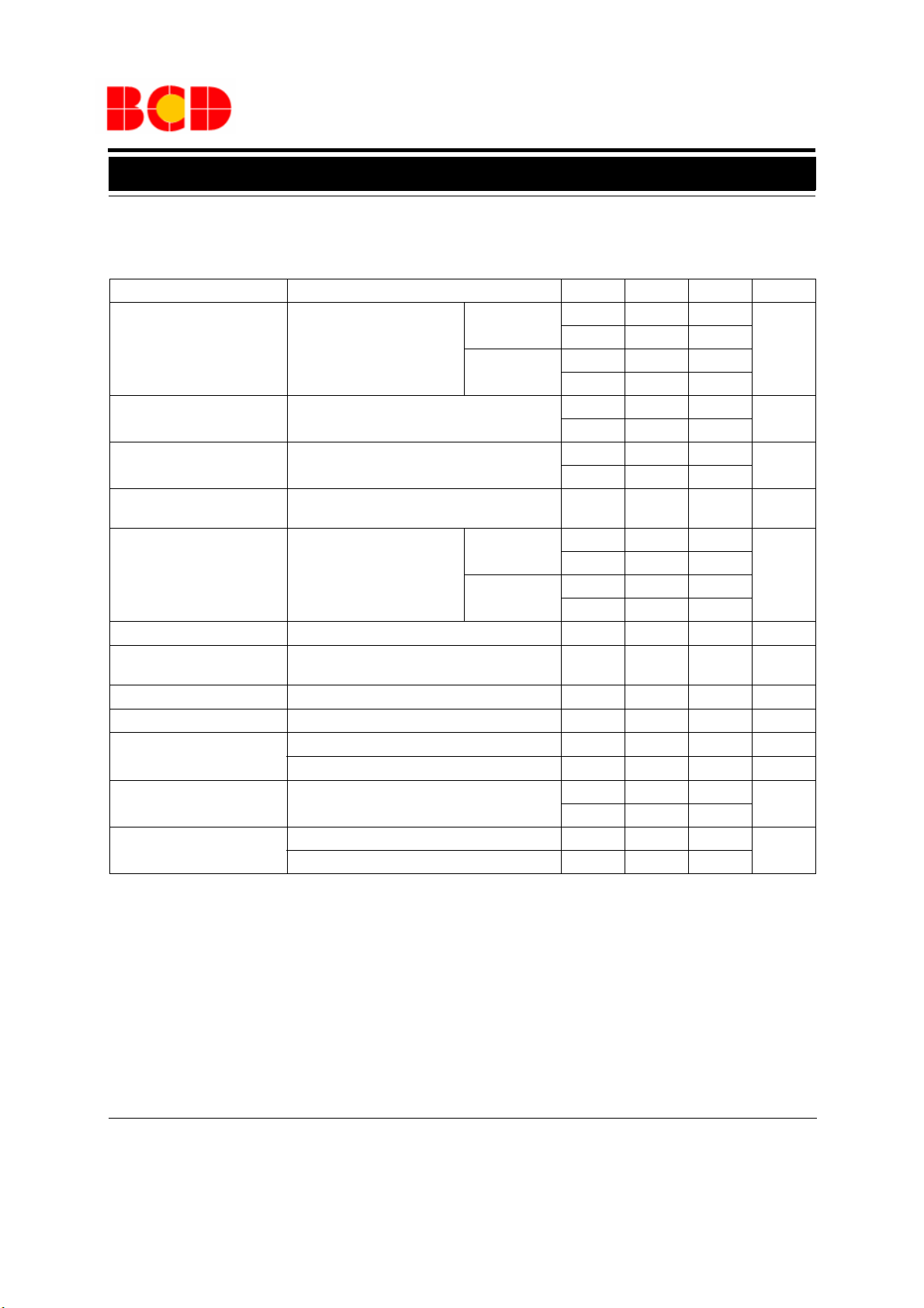
Electrical Characteristics
Limits in standard typeface are for TA=25oC, bold typeface applies over TA=-40oC to 85oC (Note 3), VCC=5V, GND=0V,
unless otherwise specified.
Parameter Conditions Min Typ Max Unit
AS393 1.0 5.0
Input Offset Voltage
Input Bias Current
Input Offset Current
Input Common Mode
Voltage Range (Note 4)
Supply Current
Voltage Gain
Large Signal Response
Time
Response Time
Output Sink Current
Output LeackageCurrent
Saturation Voltage
Thermal Resistance
(Junction to Case)
=1.4V, RS=0Ω,
V
O
=5V to 30V
V
CC
+ or IIN- with output in Linear Range,
I
IN
=0V
V
CM
I
+-IIN -, VCM=0V
IN
V
=30V
CC
R
∞
L=
=15V, RL≥15kΩ, VO=1V to 11V
V
CC
=TTL Logic Swing, V
V
IN
=5V, RL=5.1k
V
RL
=5V, RL=5.1K
V
RL
-=1V, VIN+=0, VO=1.5V
V
IN
-=0V, VIN+=1V, VO=5V
V
IN
-=0V, VIN+=1V, VO=30V
V
IN
-=1V, VIN+=0, I
V
IN
SINK
AS393A 1.0 3.0
0
V
=5V 0.6 1.0
CC
=30V 0.7 1.7
V
CC
50 200 V/mV
=1.4V,
REF
20 0 n s
6.0 16 mA
≤4mA
25 250
5.0 50
1.3 μs
0.1 nA
200 400
DIP-8 93
SOIC-8 138
7
5
400
200
VCC -1.5
2
3
1 μA
500
mV
nA
nA
mA
mV
o
C/W
V
Note 3: These specifications are limited to -40oC≤ TA ≤85oC. Limits over temperature are guaranteed by design,
but not tested in production.
Note 4: The input common-mode voltage of either input signal voltage should not be allowed to go negatively by
o
more than 0.3V (at 25
both inputs can go to +36V without damages, independent of the magnitude of the V
Jan. 2013 Rev. 2. 3
C). The upper end of the common-mode voltage range is VCC-1.5V (at 25oC), but either or
.
CC
BCD Semiconductor Manufacturing Limited
5
Page 6

Data Sheet
10m 100m 1 10 100
1E-3
0.01
0.1
1
10
Vo-Saturation Voltage (V
DC
)
IO-Output Sink Current (mA)
85oC
70oC
25oC
-40oC
0 5 10 15 20 2 5 30 35 40
0.0
0.1
0.2
0.3
0.4
0.5
0.6
0.7
0.8
0.9
1.0
Supply Current (mA)
Supply Voltage (V)
Ta=-40oC
Ta=0oC
Ta=25oC
Ta=70oC
Ta=85oC
0.0 5.0 10.0 15.0 20.0 25.0 30.0
0
10
20
30
40
50
60
70
80
90
100
Input Bias Current (nA)
Supply Voltage (V)
-40 oC
0 oC
25 oC
70 oC
85 oC
V
IN
V
CC
5.1K
V
OUT
+
_
LOW POWER LOW OFFSET VOLTAGE DUAL COMPARATORS AS393/393A
Typical Performance Characteristics
Figure 4. Supply Voltage vs. Supply Current Figure 5. Supply Voltage vs. Input Bias Current
6
4
2
0
Output Voltage (V)
0
-50
-100
Input Voltage (mV)
0
0.4
0.80.2
1.0
1.20.6
1.6
1.8
2.01.4
Time (μs)
Figure 7. Response Time for 5mV Input Overdrive - Figure 6. Output Sink Current vs. Saturation Voltage
Negative Transition
Jan. 2013 Rev. 2. 3
BCD Semiconductor Manufacturing Limited
6
Page 7

Data Sheet
+V
IN
+V
REF
1/2 AS393/A
V
CC
3K
V
O
+
-
100K
5V
+
-
4
8
1/2 AS393/A
+V
IN
+V
REF
V
O
V
IN
V
CC
5.1K
V
OUT
+
_
LOW POWER LOW OFFSET VOLTAGE DUAL COMPARATORS AS393/393A
Typical Performance Characteristics (Continued)
5
0
Output Voltage (V)
100
0
Input Voltage (mV)
0.4
0
0.80.2
Figure 8. Response Time for 5mV Input Overdrive -
Positive Transition
1.20.6
1.0
Time (μs)
1.6
1.8
2.01.4
Typical Applications
Figure 9. Basic Comparator
Jan. 2013 Rev. 2. 3
7
Figure 10. Driving CMOS
BCD Semiconductor Manufacturing Limited
Page 8

Data Sheet
1M
1M
1M
V
CC
V
O
10K
-
+
+V
IN
100pF
0.001μF
1/2 AS393/A
100K
75pF
100K
V
CC
4.3K
V
O
100K
100K
-
+
V
IN
1/2 AS393/A
LOW POWER LOW OFFSET VOLTAGE DUAL COMPARATORS AS393/393A
Typical Applications (Continued)
Figure 11. One Shot Multivibrator
Figure 12. Squarewave Oscillator
Jan. 2013 Rev. 2. 3
BCD Semiconductor Manufacturing Limited
8
Page 9

Data Sheet
4
°
6
°
R0.750(0.030)
0.254(0.010)TYP
0.130(0.005)MIN
8.200(0.323)
9.400(0.370)
0.204(0.008)
0.360(0.014)
7.620(0.300)TYP
4
°
6
°
5°
0.700(0.028)
9.000(0.354)
9.600(0.378)
3.710(0.146)
4.310(0.170)
3.000(0.118)
3.600(0.142)
0.360(0.014)
0.560(0.022)
2.540(0.100) TYP
6.200(0.244)
6.600(0.260)
3.200(0.126)
3.600(0.142)
0.510(0.020)MIN
Φ3.000(0.118)
Depth
0.100(0.004)
0.200(0.008)
1.524(0.060) TYP
Note: Eject hole, oriented hole and mold mark is optional.
LOW POWER LOW OFFSET VOLTAGE DUAL COMPARATORS AS393/393A
Mechanical Dimensions
DIP-8 Unit: mm(inch)
Jan. 2013 Rev. 2. 3
BCD Semiconductor Manufacturing Limited
9
Page 10

Data Sheet
1.500(0.059)
1.700(0.067)
3.300(0.130)MAX
0.600(0.024)
0.800(0.031)
0.940(0.037)
1.040(0.041)
1.470(0.058)
1.670(0.066)
2.540(0.100)
BCS
3.100(0.122)
3.500(0.138)
7.570(0.298)
8.200(0.323)
8.200(0.323)
9.400(0.370)
9.150(0.360)
9.350(0.368)
6.250(0.246)
6.450(0.254)
0.500(0.020)MIN
0.390(0.015)
0.550(0.022)
Note: Eject hole, oriented hole and mold mark is optional.
LOW POWER LOW OFFSET VOLTAGE DUAL COMPARATORS AS393/393A
Mechanical Dimensions (Continued)
TDIP-8 Unit: mm(inch)
Jan. 2013 Rev. 2. 3
BCD Semiconductor Manufacturing Limited
10
Page 11

Data Sheet
0
°
8
°
1°
5°
R
0
.
1
5
0
(
0
.
0
0
6
)
R0.150(0.006)
1.000(0.039)
0.330(0.013)
0.510(0.020)
1.350(0.053)
1.750(0.069)
0.100(0.004)
0.300(0.012)
0.900(0.035)
0.800(0.031)
0.200(0.008)
3.800(0.150)
4.000(0.157)
7
°
7
°
2
0
:
1
D
1.270(0.050)
TYP
0.190(0.007)
0.250(0.010)
8
°
D
5.800(0.228)
6.200(0.244)
0.675(0.027)
0.725(0.029)
0.320(0.013)
8
°
0.450(0.017)
0.800(0.031)
4.700(0.185)
5.100(0.201)
Note: Eject hole, oriented hole and mold mark is optional.
LOW POWER LOW OFFSET VOLTAGE DUAL COMPARATORS AS393/393A
Mechanical Dimensions (Continued)
SOIC-8 Unit: mm(inch)
Jan. 2013 Rev. 2. 3
11
BCD Semiconductor Manufacturing Limited
Page 12

Data Sheet
4.300(0.169)
0.400(0.016)
0.190(0.007)
0.300(0.012)
SEE DETAIL A
DETAIL A
2.900(0.114)
0.050(0.002)
0.150(0.006)
1.200(0.047)
MAX
1.950(0.077)
0°
8°
12 °
TOP & BOTTOM
R0.090(0.004)
0.450(0.018)
0.750(0.030)
1.000(0.039)
6.400(0.252)
0.800(0.031)
1.050(0.041)
0.090(0.004)
0.200(0.008)
GAGE PLANE
SEATING
PLANE
0.250(0.010)
3.100(0.122)
4.500(0.177)
TYP
0.650(0.026)
TYP
TYP
TYP
R0.090(0.004)
REF
Note: Eject hole, oriented hole and mold mark is optional.
LOW POWER LOW OFFSET VOLTAGE DUAL COMPARATORS AS393/393A
Mechanical Dimensions (Continued)
TSSOP-8 Unit: mm(inch)
Jan. 2013 Rev. 2. 3
12
BCD Semiconductor Manufacturing Limited
Page 13

Data Sheet
4.700(0.185)
0.650(0.026)TYP
5.100(0.201)
0.410(0.016)
0.650(0.026)
0
.
0
0
0
(
0
.
0
0
0
)
0
.
2
0
0
(
0
.
0
0
8
)
0.300(0.012)TYP
3
.
1
0
0
(
0
.
1
2
2
)
2
.
9
0
0
(
0
.
1
1
4
)
0
.
8
0
0
(
0
.
0
3
1
)
1
.
2
0
0
(
0
.
0
4
7
)
3.100(0.122)
2.900(0.114)
0
°
6
°
0
.
1
5
0
(
0
.
0
0
6
)
T
Y
P
0
.
7
6
0
(
0
.
0
3
0
)
0
.
9
7
0
(
0
.
0
3
8
)
`
Note: Eject hole, oriented hole and mold mark is optional.
LOW POWER LOW OFFSET VOLTAGE DUAL COMPARATORS AS393/393A
Mechanical Dimensions (Continued)
MSOP-8 Unit: mm(inch)
Jan. 2013 Rev. 2. 3
13
BCD Semiconductor Manufacturing Limited
Page 14

BCD Semiconductor Manufacturing Limited
IMPORTANT NOTICE
IMPORTANT NOTICE
BCD Semiconductor Manufacturing Limited reserves the right to make changes without further notice to any products or specifi-
BCD Semiconductor Manufacturing Limited reserves the right to make changes without further notice to any products or specifi-
cations herein. BCD Semiconductor Manufacturing Limited does not assume any responsibility for use of any its products for any
cations herein. BCD Semiconductor Manufacturing Limited does not assume any responsibility for use of any its products for any
particular purpose, nor does BCD Semiconductor Manufacturing Limited assume any liability arising out of the application or use
particular purpose, nor does BCD Semiconductor Manufacturing Limited assume any liability arising out of the application or use
of any its products or circuits. BCD Semiconductor Manufacturing Limited does not convey any license under its patent rights or
of any its products or circuits. BCD Semiconductor Manufacturing Limited does not convey any license under its patent rights or
other rights nor the rights of others.
other rights nor the rights of others.
http://www.bcdsemi.com
MAIN SITE
MAIN SITE
- Headquarters
BCD Semiconductor Manufacturing Limited
BCD Semiconductor Manufactur ing Limited
- Wafer Fab
No. 1600, Zi Xing Road, Shanghai ZiZhu Science-based Industrial Park, 200241, China
Shanghai SIM-BCD Semiconductor Manufacturing Limited
Tel: +86-21-24162266, Fax: +86-21-24162277
800, Yi Shan Road, Shanghai 200233, China
Tel: +86-21-6485 1491, Fax: +86-21-5450 0008
REGIONAL SALES OFFICE
Shenzhen Office
REGIONAL SALES OFFICE
Shanghai SIM-BCD Semiconductor Manufacturing Co., Ltd., Shenzhen Office
Shenzhen Office
Unit A Room 1203, Skyworth Bldg., Gaoxin Ave.1.S., Nanshan District, Shenzhen,
Shanghai SIM-BCD Semiconductor Manufacturing Co., Ltd. Shenzhen Office
China
Advanced Analog Circuits (Shanghai) Corporation Shenzhen Office
Tel: +86-755-8826 7951
Room E, 5F, Noble Center, No.1006, 3rd Fuzhong Road, Futian District, Shenzhen 518026, China
Fax: +86-755-8826 7865
Tel: +86-755-8826 7951
Fax: +86-755-8826 7865
- Wafer Fab
BCD Semiconductor Manufacturing Limited
Shanghai SIM-BCD Semiconductor Manufacturing Co., Ltd.
- IC Design Group
800 Yi Shan Road, Shanghai 200233, China
Advanced Analog Circuits (Shanghai) Corporation
Tel: +86-21-6485 1491, Fax: +86-21-5450 0008
8F, Zone B, 900, Yi Shan Road, Shanghai 200233, China
Tel: +86-21-6495 9539, Fax: +86-21-6485 9673
Taiwan Office
BCD Semiconductor (Taiwan) Company Limited
Taiwan Office
4F, 298-1, Rui Guang Road, Nei-Hu District, Taipei,
BCD Semiconductor (Taiwan) Company Limited
Tai wan
4F, 298-1, Rui Guang Road, Nei-Hu District, Taipei,
Tel: +886-2-2656 2808
Taiwan
Fax: +886-2-2656 2806
Tel: +886-2-2656 2808
Fax: +886-2-2656 2806
USA Office
BCD Semiconductor Corp.
USA Office
30920 Huntwood Ave. Hayward,
BCD Semiconductor Corporation
CA 94544, USA
30920 Huntwood Ave. Hayward,
Tel : +1-510-324-2988
CA 94544, U.S.A
Fax: +1-510-324-2788
Tel : +1-510-324-2988
Fax: +1-510-324-2788
 Loading...