

Page 1
Data Sheet
LOW POWER DUAL OPERATIONAL AMPLIFIERS AS358/358A
General Description
The AS358/358A consist of two independent, high
gain and internally frequency compensated operational
amplifiers, they are specifically designed to operate
from a single power supply. Operation from split
power supply is also possible and the low power supply current drain is independent of the magnitude of
the power supply voltages. Typical applications
include transducer amplifiers, DC gain blocks and
most conventional operational amplifier circuits.
The AS358/358A series are compatible with industry
standard 358. AS358A has more stringent input offset
voltage than AS358.
The AS358 is available in DIP-8, TDIP-8, SOIC-8,
TSSOP-8 and MSOP-8 packages, AS358A is available
in DIP-8 and SOIC-8 packages.
Features
· Internally Frequency Compensated for Unity
Gain
· Large Voltage Gain: 100dB (Typical)
· Low Input Bias Current: 20nA (Typical)
· Low Input Offset Voltage: 2mV (Typical)
· Low Supply Current: 0.5mA (Typical)
· Wide Power Supply Voltage:
Single Supply: 3V to 36V
Dual Supplies: ± 1.5V to ± 18V
· Input Common Mode Voltage Range Includes
Ground
· Large Output Voltage Swing: 0V to V
CC
-1.5V
Applications
· Battery Charger
· Cordless Telephone
· Switching Power Supply
SOIC-8
DIP-8
TSSOP-8
Figure 1. Package Types of AS358/358A
BCD Semiconductor Manufacturing LimitedJan. 2013 Rev. 2. 2
1
TDIP-8
MSOP-8
Page 2
Data Sheet
Q2
Q4
Q3
Q1
Q8
Q9
6μA
4μA
Q10
Q11
50μA
Q5
Q6
Q13
Rsc
Cc
100μA
Q7
INPUTS
+
-
OUTPUT
Q12
V
CC
1
2
3
4
8
7
6
5
1
2
3
4
8
7
6
5
LOW POWER DUAL OPERATIONAL AMPLIFIERS AS358/358A
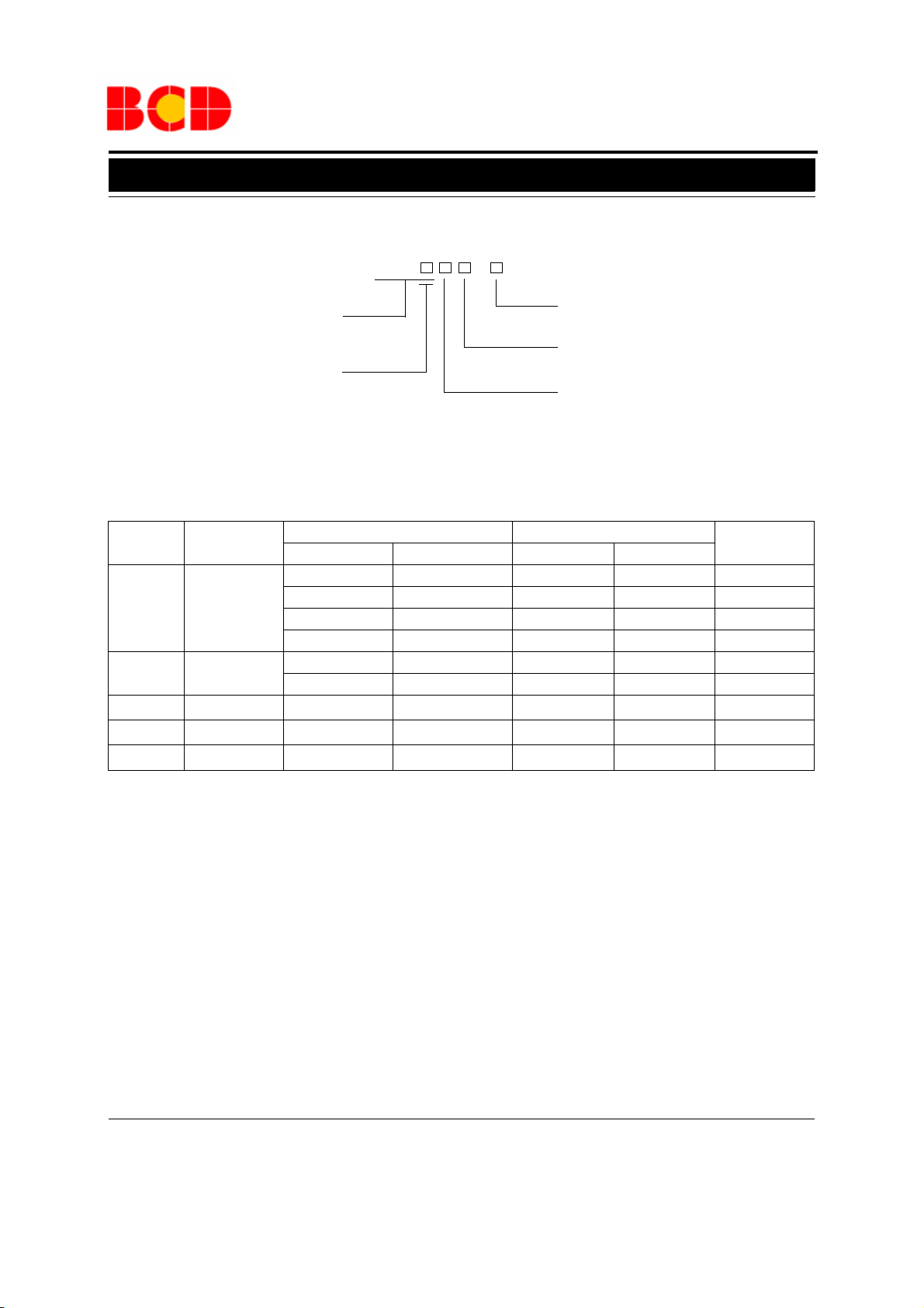
Pin Configuration
M/G/MM Package
(SOIC-8/TSSOP-8/MSOP-8)
OUTPUT 1
INPUT 1-
INPUT 1+
GND
Figure 2. Pin Configuration of AS358/358A (Top View)
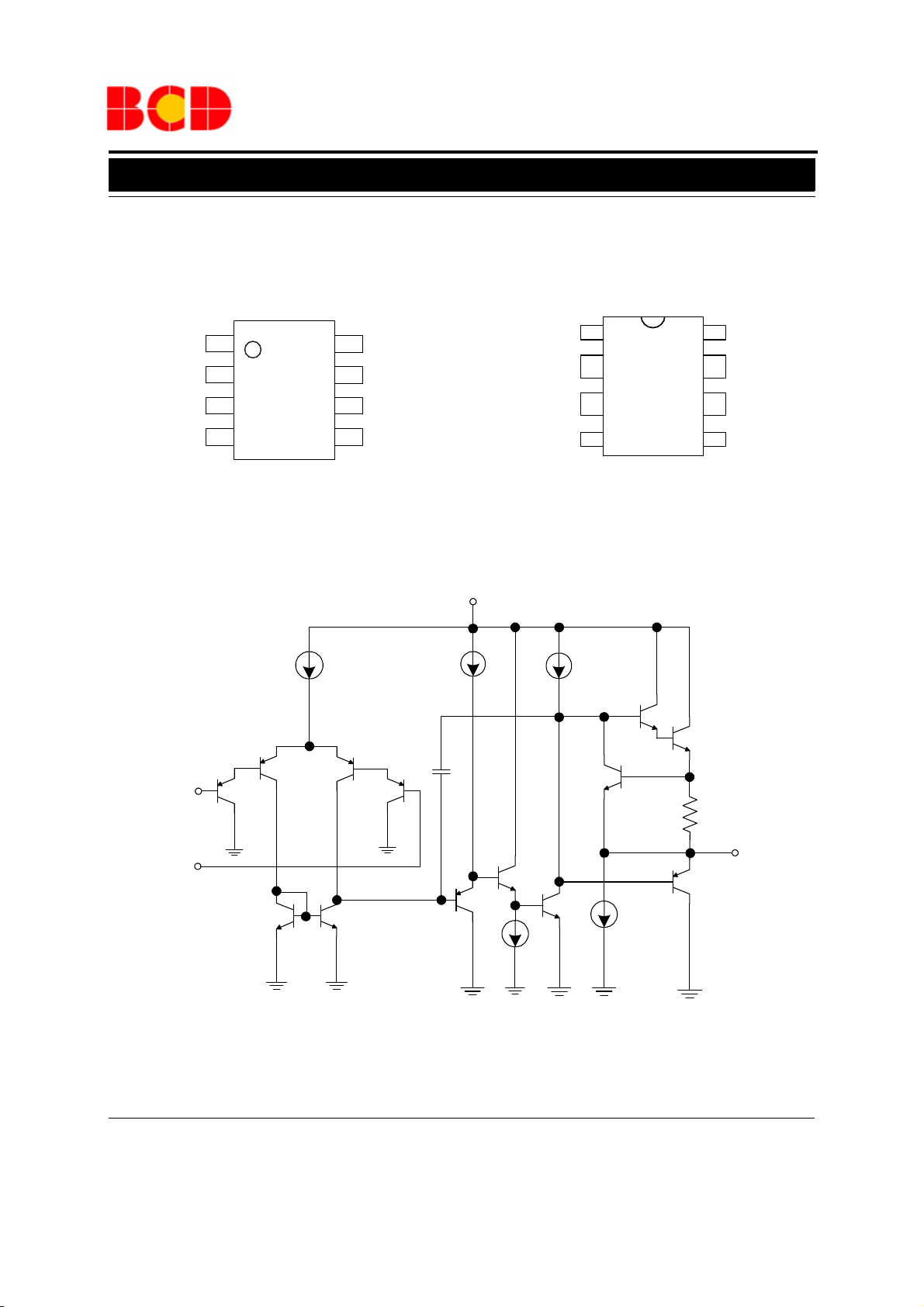
Functional Block Diagram
V
CC
OUTPUT 2
INPUT 2-
INPUT 2+
OUTPUT 1
INPUT 1-
INPUT 1+
GND
P/PT Package
(DIP-8/TDIP-8)
V
CC
OUTPUT 2
INPUT 2-
INPUT 2+
Figure 3. Functional Block Diagram of AS358/358A
(Each Amplifier)
2
BCD Semiconductor Manufacturing LimitedJan. 2013 Rev. 2. 2
Page 3
Data Sheet
LOW POWER DUAL OPERATIONAL AMPLIFIERS AS358/358A
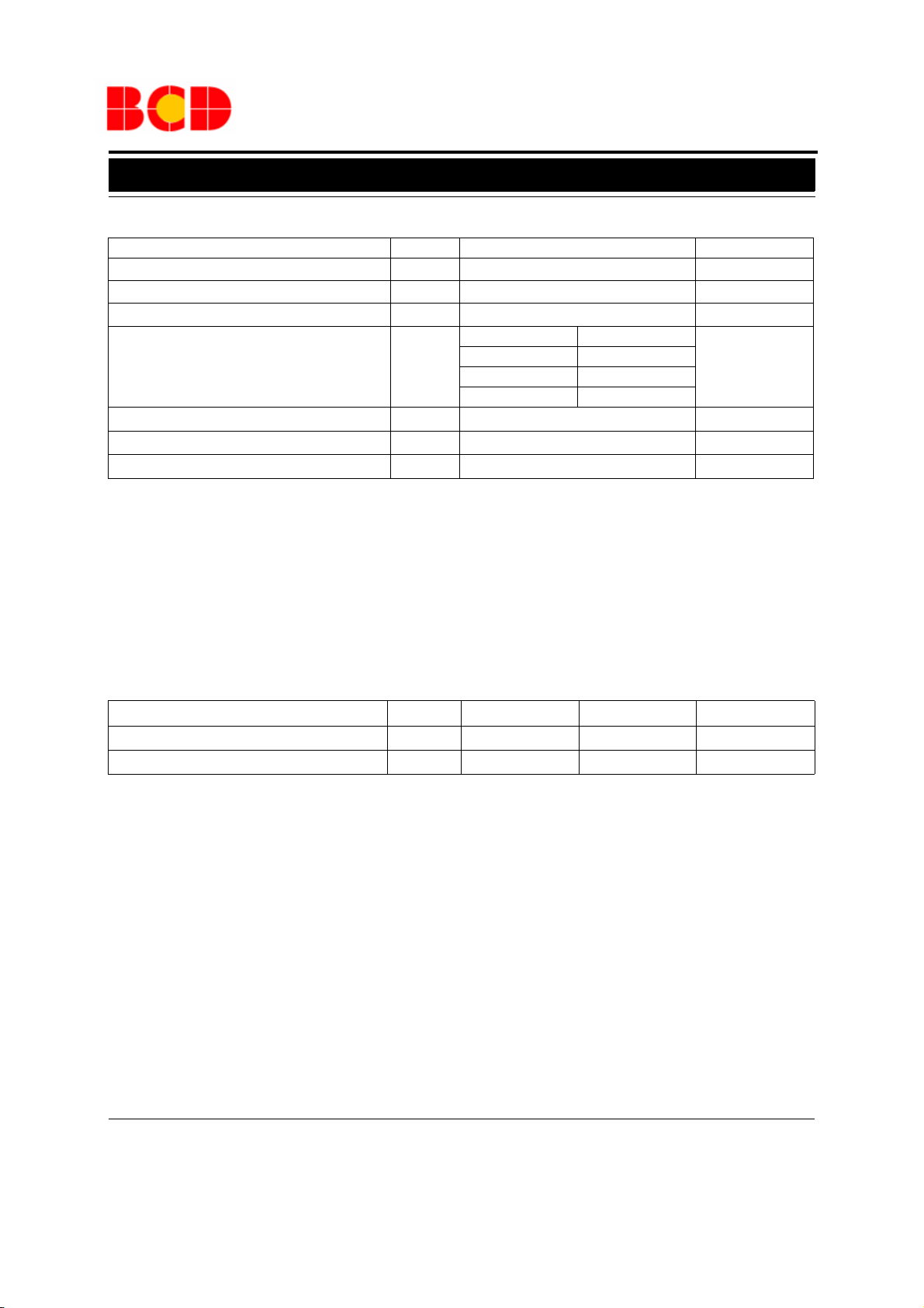
Ordering Information
Package
SOIC-8
DIP-8
TDIP-8
TSSOP-8
MSOP-8
Circuit Type
Blank: AS358
A: AS358A
Temperature
Range
o
-40 to 85
-40 to 85
-40 to 85
-40 to 85
-40 to 85
C
o
C
o
C
o
C
o
C
AS358
-
E1: Lead Free
G1: Green
TR: Tape and Reel
Blank: Tube
Package
M: SOIC-8
P: DIP-8
PT: TDIP-8
G: TSSOP-8
MM: MSOP-8
Part Number Marking ID
Lead Free Green Lead Free Green
AS358M-E1 AS358M-G1 AS358M-E1 AS358M-G1 Tube
AS358MTR-E1 AS358MTR-G1 AS358M-E1 AS358M-G1 Tape & Reel
AS358AM-E1 AS358AM-G1 AS358AM-E1 AS358AM-G1 Tube
AS358AMTR-E1 AS358AMTR-G1 AS358AM-E1 AS358AM-G1 Tape & Reel
AS358P-E1 AS358P-G1 AS358P-E1 AS358P-G1 Tube
AS358AP-E1 AS358AP-G1 AS358AP-E1 AS358AP-G1 Tube
AS358PT-G1 AS358PT-G1
AS358GTR-E1 AS358GTR-G1 EG3A GG3A
AS358MMTR-E1 AS358MMTR-G1 AS358MM-E1 AS358MM-G1
Packing Type
Tube
Tap e & Ree l
Tap e & Ree l
BCD Semiconductor's Pb-free products, as designated with "E1" suffix in the part number, are RoHS compliant. Products with
"G1" suffix are available in green packages.
BCD Semiconductor Manufacturing LimitedJan. 2013 Rev. 2. 2
3
Page 4
Data Sheet
LOW POWER DUAL OPERATIONAL AMPLIFIERS AS358/358A
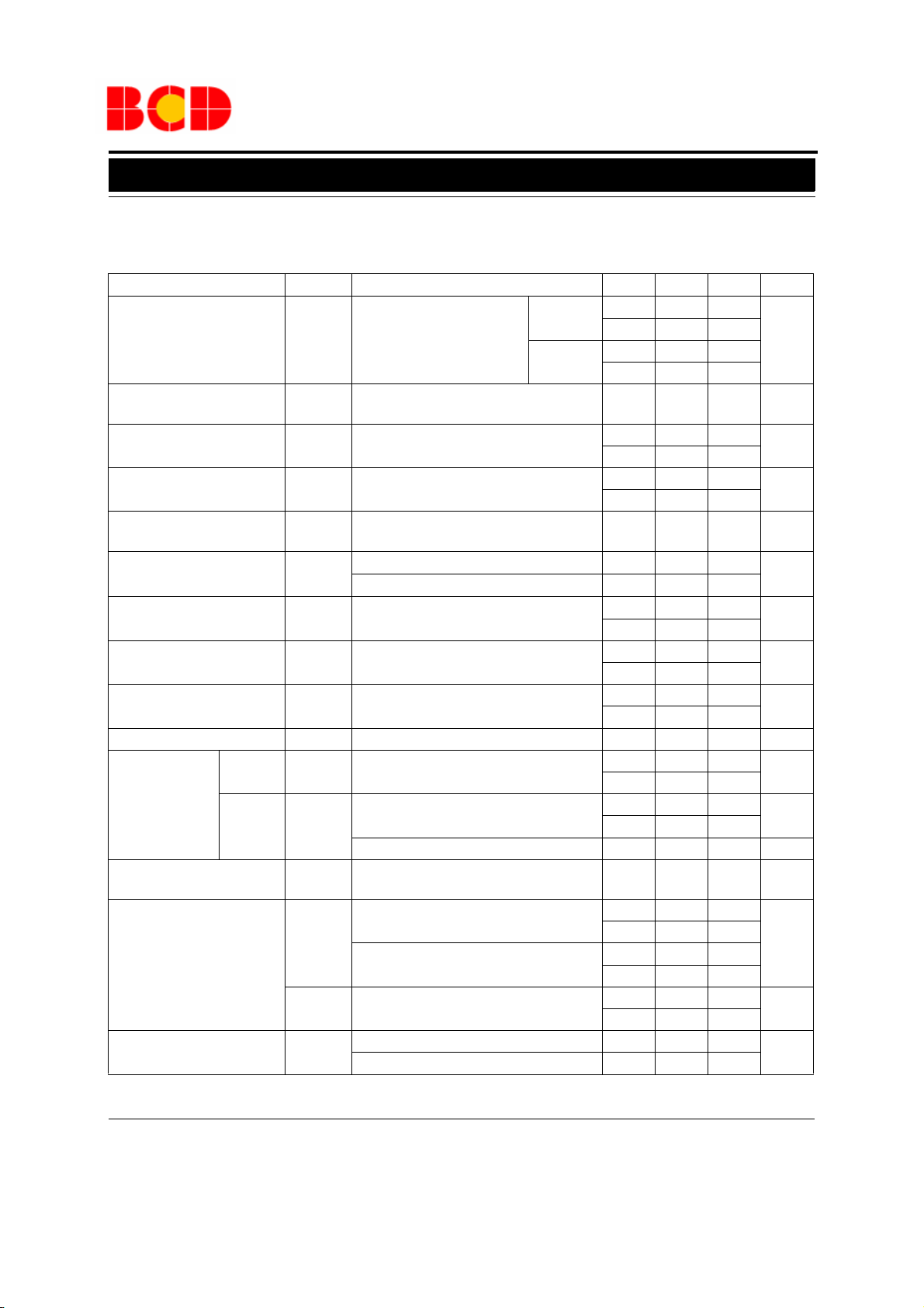
Absolute Maximum Ratings (Note 1)
Parameter Symbol Value Unit
Power Supply Voltage
Differential Input Voltage
Input Voltage
Power Dissipation (T
=25oC)
A
Operating Junction Temperature
Storage Temperature Range
Lead Temperature (Soldering, 10 Seconds)
Note 1: Stresses greater than those listed under "Absolute Maximum Ratings" may cause permanent damage to the device.
These are stress ratings only, and functional operation of the device at these or any other conditions beyond those indicated
under "Recommended Operating Conditions" is not implied. Exposure to "Absolute Maximum Ratings" for extended periods
may affect device reliability.
V
V
V
T
T
LEAD
CC
ID
IC
P
D
T
STG
40 V
40 V
-0.3 to 40 V
DIP-8 830
SOIC-8 550
TSSOP-8 500
mW
MSOP-8 470
J
150
-65 to 150
260
o
C
o
C
o
C
Recommended Operating Conditions
Parameter Symbol Min Max Unit
Supply Voltage V
Ambient Operating Temperature Range T
CC
A
336V
-40 85
o
C
BCD Semiconductor Manufacturing LimitedJan. 2013 Rev. 2. 2
4
Page 5
Data Sheet
LOW POWER DUAL OPERATIONAL AMPLIFIERS AS358/358A
Electrical Characteristics
Limits in standard typeface are for TA=25oC, bold typeface applies over -40oC to 85oC (Note 2), VCC=5V, GND=0V, unless
otherwise specified.
Parameter Symbol Test Conditions Min Typ Max Unit
AS358
AS358A
0
85 100
80
60 70
60
70 100
60
Input Offset Voltage
Average Temperature Coefficient of Input Offset Voltage
Input Bias Current
Input Offset Current
Input Common Mode Voltage
Range (Note 3)
Supply Current
Large Signal Voltage Gain
Common Mode Rejection
Ratio
Power Supply Rejection
Ratio
V
IO
/ΔT
ΔV
IO
I
BIASIIN
I
IO
V
IR
I
CC
G
V
CMRR
PSRR
VO=1.4V, RS=0Ω,
=5V to 30V
V
CC
T
=-40 to 85oC
A
+ or IIN-, VCM=0V
IIN+ - IIN-, VCM=0V
VCC=30V
TA=-40 to 85oC, RL=∞, VCC=30V
T
=-40 to 85oC, RL=∞, VCC=5V
A
VCC=15V, VO=1V to 11V, RL ≥ 2kΩ
DC, V
V
=0V to (VCC-1.5)V
CM
=5V to 30V
CC
Channel Separation CS f=1kHz to 20kHz -120 dB
Source
Output Current
Sink
Output Short Circuit Current
to Ground
Output Voltage Swing
Thermal Resistance
(Junction to Case)
I
SOURCEVIN
I
SINK
I
SC
V
OH
V
OL
θ
JC
+=1V, VIN-=0V, VCC=15V, VO=2V
VIN+=0V, VIN-=1V, VCC=15V, VO=2V
V
+=0V,VIN-=1V,VCC=15V, VO=0.2V 12 50 μA
IN
VCC=15V
VCC=30V, RL=2kΩ
V
=30V, RL=10kΩ
CC
VCC=5V, RL= 10kΩ
DIP-8 53
SOIC-8 78
20 40
20
10 15
5
26
26
27 28
27
25
7
23
mV
5
7
20 200
530
V
0.7 2
0.5 1.2
200
100
CC
-1.5
μV/
nA
nA
V
mA
dB
dB
dB
mA
mA
40 60 mA
V
520
mV
30
o
C/W
o
C
Note 2: Limits over the full temperature are guaranteed by design, but not tested in production.
BCD Semiconductor Manufacturing LimitedJan. 2013 Rev. 2. 2
5
Page 6

Data Sheet
0 5 10 15
0
5
10
15
POSITIVE
NEGATIVE
Input Voltage (+V
DC
)
Power Supply Voltage (+VDC)
-25 0 25 50 75 100 125
0
2
4
6
8
10
12
14
16
18
20
Input Current (nA)
Temperature (oC)
0 5 10 15 20 25 30 35 40
0.0
0.1
0.2
0.3
0.4
0.5
0.6
0.7
0.8
0.9
1.0
Supply Current (mA)
Supply Voltage (V)
0 8 16 24 32 40
60
75
90
105
120
Power Supply Voltage (V)
Voltage Gain (dB)
RL=2KΩ
RL=20KΩ
LOW POWER DUAL OPERATIONAL AMPLIFIERS AS358/358A
Electrical Characteristics (Continued)
Note 3: The input common-mode voltage of either input signal voltage should not be allowed to go negatively by
more than 0.3V (at 25
o
C). The upper end of the common-mode voltage range is V
CC
both inputs can go to +36V without damages, independent of the magnitude of the V
-1.5V (at 25
.
CC
o
C), but either or
Typical Performance Characteristics
Figure 4. Input Voltage Range Figure 5. Input Current
Figure 6. Supply Current Figure 7. Voltage Gain
BCD Semiconductor Manufacturing LimitedJan. 2013 Rev. 2. 2
6
Page 7

Data Sheet
1 10 100 1k 10k 100k 1M
0
10
20
30
40
50
60
70
80
90
100
110
120
Voltage Gain (dB)
Frequency (Hz)
1k 10k 100k 1M
0
5
10
15
20
Frequency (Hz)
Output Swing (V)
LOW POWER DUAL OPERATIONAL AMPLIFIERS AS358/358A
Typical Performance Characteristics (Continued)
4
3
2
Output
1
0
3
2
1
Input
0
Voltage (V) Voltage (V)
0 4 8 1216202428323640
Time (μs)
Figure 8. Open Loop Frequency Response Figure 9. Voltage Follower Pulse Response
800
700
600
500
400
300
200
Output Voltage (mV)
100
04
812
Time (μs)
Figure 10. Voltage Follower Pulse Response
(Small Signal)
16 20
Figure 11. Large Signal Frequency Response
BCD Semiconductor Manufacturing LimitedJan. 2013 Rev. 2. 2
7
Page 8

Data Sheet
-25 0 25 50 75 100 125
0
10
20
30
40
50
60
70
80
90
100
Output Current (mA)
Temperature (oC)
1E-3 0.01 0.1 1 10 100
0.01
0.1
1
10
VCC=15V
Output Voltage (V)
Output Sink Current (mA)
VCC=5V
0.1 1 10 100
0
1
2
3
4
5
6
7
8
Output Voltage Referenced to Vcc (V)
Output Source Current (mA)
LOW POWER DUAL OPERATIONAL AMPLIFIERS AS358/358A
Typical Performance Characteristics (Continued)
Figure 12. Output Characteristics: Current Sourcing
Figure 14. Current Limiting
Figure 13. Output Characteristics: Current Sinking
BCD Semiconductor Manufacturing LimitedJan. 2013 Rev. 2. 2
8
Page 9

Data Sheet
R6 100k
V
O
R5
100k
R1 100k
R2 100k
R3 100k
R4 100k
+V
1
+V
2
+V
3
+V
4
1/2 AS358/A
+
-
AC
Line
SMPS
R2
Current
Sense
R7
R8
Battery
Pack
R4
R3
AZ431
R5
R1
Opto
Isolator
V
CC
GND
GND
1/2
AS358/A
+
1/2
AS358/A
R6
+
-
V
CC
R1 910K
V
O
R2 100K
R3 91K
V
IN(+)
V
CC
R
L
1/2 AS358/A
-
+
LOW POWER DUAL OPERATIONAL AMPLIFIERS AS358/358A
Typical Application
Figure 15. Battery Charger
Figure 17. DC Summing AmplifierFigure 16. Power Amplifier
BCD Semiconductor Manufacturing LimitedJan. 2013 Rev. 2. 2
9
Page 10

Data Sheet
V
CC
R4
3K
R3
2K
+
-
2V
+
-
2V
I1 I 2
1mA
1/2 AS358/A
R1
2K
R2
-
+
R5 100k
R3 100k
R2 100k
R1 1M
V
O
V
CC
1/2 AS358/A
0.001μF
-
+
R4
100k
V
O
R2 16kR1 16K
V
IN
R3
100k
1/2 AS358/A
R4
100k
C2
0.01μF
C1 0.01μF
f
O
V
O
0
f
O
=1kHz
Q=1
A
V
=2
+
-
R4 100k
V
CC
R3
1M
R1 100k
R2 1M
C1
0.1μF
C
IN
R5
100k
C
O
V
O
1/2 AS358/ A
R
L
10k
C2
10μF
A
V
=1+R2/R1
A
V
=11 (As shown)
-
+
AC
R
B
6.2k
LOW POWER DUAL OPERATIONAL AMPLIFIERS AS358/358A
Typical Application (Continued)
Figure 18. AC Coupled Non-Inverting Amplifier
Figure 20. Pulse Generator
Figure 19. Fixed Current Sources
Figure 21. DC Coupled Low-Pass Active Filter
BCD Semiconductor Manufacturing LimitedJan. 2013 Rev. 2. 2
10
Page 11

Data Sheet
4
°
6
°
R0.750(0.030)
0.254(0.010)TYP
0.130(0.005)MIN
8.200(0.323)
9.400(0.370)
0.204(0.008)
0.360(0.014)
7.620(0.300)TYP
4
°
6
°
5°
0.700(0.028)
9.000(0.354)
9.600(0.378)
3.710(0.146)
4.310(0.170)
3.000(0.118)
3.600(0.142)
0.360(0.014)
0.560(0.022)
2.540(0.100) TYP
6.200(0.244)
6.600(0.260)
3.200(0.126)
3.600(0.142)
0.510(0.020)MIN
Φ3.000(0.118)
Depth
0.100(0.004)
0.200(0.008)
1.524(0.060) TYP
Note: Eject hole, oriented hole and mold mark is optional.
LOW POWER DUAL OPERATIONAL AMPLIFIERS AS358/358A
Mechanical Dimensions
DIP-8 Unit: mm(inch)
BCD Semiconductor Manufacturing LimitedJan. 2013 Rev. 2. 2
11
Page 12

Data Sheet
1.500(0.059)
1.700(0.067)
3.300(0.130)MAX
0.600(0.024)
0.800(0.031)
0.940(0.037)
1.040(0.041)
1.470(0.058)
1.670(0.066)
2.540(0.100)
BCS
3.100(0.122)
3.500(0.138)
7.570(0.298)
8.200(0.323)
8.200(0.323)
9.400(0.370)
9.150(0.360)
9.350(0.368)
6.250(0.246)
6.450(0.254)
0.500(0.020)MIN
0.390(0.015)
0.550(0.022)
Note: Eject hole, oriented hole and mold mark is optional.
LOW POWER DUAL OPERATIONAL AMPLIFIERS AS358/358A
Mechanical Dimensions (Continued)
TDIP-8 Unit: mm(inch)
BCD Semiconductor Manufacturing LimitedJan. 2013 Rev. 2. 2
12
Page 13

Data Sheet
0
°
8
°
1°
5°
R
0
.
1
5
0
(
0
.
0
0
6
)
R0.150(0.006)
1.000(0.039)
0.330(0.013)
0.510(0.020)
1.350(0.053)
1.750(0.069)
0.100(0.004)
0.300(0.012)
0.900(0.035)
0.800(0.031)
0.200(0.008)
3.800(0.150)
4.000(0.157)
7
°
7
°
2
0
:
1
D
1.270(0.050)
TYP
0.190(0.007)
0.250(0.010)
8
°
D
5.800(0.228)
6.200(0.244)
0.675(0.027)
0.725(0.029)
0.320(0.013)
8
°
0.450(0.017)
0.800(0.031)
4.700(0.185)
5.100(0.201)
Note: Eject hole, oriented hole and mold mark is optional.
LOW POWER DUAL OPERATIONAL AMPLIFIERS AS358/358A
Mechanical Dimensions (Continued)
SOIC-8 Unit: mm(inch)
φ
13
BCD Semiconductor Manufacturing LimitedJan. 2013 Rev. 2. 2
Page 14

Data Sheet
4.300(0.169)
0.400(0.016)
0.190(0.007)
0.300(0.012)
SEE DETAIL A
DETAIL A
2.900(0.114)
0.050(0.002)
0.150(0.006)
1.200(0.047)
MAX
1.950(0.077)
0°
8°
12 °
TOP & BOTTOM
R0.090(0.004)
0.450(0.018)
0.750(0.030)
1.000(0.039)
6.400(0.252)
0.800(0.031)
1.050(0.041)
0.090(0.004)
0.200(0.008)
GAGE PLANE
SEATING
PLANE
0.250(0.010)
3.100(0.122)
4.500(0.177)
TYP
0.650(0.026)
TYP
TYP
TYP
R0.090(0.004)
REF
Note: Eject hole, oriented hole and mold mark is optional.
LOW POWER DUAL OPERATIONAL AMPLIFIERS AS358/358A
Mechanical Dimensions (Continued)
TSSOP-8 Unit: mm(inch)
14
BCD Semiconductor Manufacturing LimitedJan. 2013 Rev. 2. 2
Page 15

Data Sheet
4.700(0.185)
0.650(0.026)TYP
5.100(0.201)
0.410(0.016)
0.650(0.026)
0
.
0
0
0
(
0
.
0
0
0
)
0
.
2
0
0
(
0
.
0
0
8
)
0.300(0.012)TYP
3
.
1
0
0
(
0
.
1
2
2
)
2
.
9
0
0
(
0
.
1
1
4
)
0
.
8
0
0
(
0
.
0
3
1
)
1
.
2
0
0
(
0
.
0
4
7
)
3.100(0.122)
2.900(0.114)
0
°
6
°
0
.
1
5
0
(
0
.
0
0
6
)
T
Y
P
0
.
7
6
0
(
0
.
0
3
0
)
0
.
9
7
0
(
0
.
0
3
8
)
`
Note: Eject hole, oriented hole and mold mark is optional.
LOW POWER DUAL OPERATIONAL AMPLIFIERS AS358/358A
Mechanical Dimensions (Continued)
MSOP-8 Unit: mm(inch)
BCD Semiconductor Manufacturing LimitedJan. 2013 Rev. 2. 2
15
Page 16

BCD Semiconductor Manufacturing Limited
IMPORTANT NOTICE
IMPORTANT NOTICE
BCD Semiconductor Manufacturing Limited reserves the right to make changes without further notice to any products or specifi-
BCD Semiconductor Manufacturing Limited reserves the right to make changes without further notice to any products or specifi-
cations herein. BCD Semiconductor Manufacturing Limited does not assume any responsibility for use of any its products for any
cations herein. BCD Semiconductor Manufacturing Limited does not assume any responsibility for use of any its products for any
particular purpose, nor does BCD Semiconductor Manufacturing Limited assume any liability arising out of the application or use
particular purpose, nor does BCD Semiconductor Manufacturing Limited assume any liability arising out of the application or use
of any its products or circuits. BCD Semiconductor Manufacturing Limited does not convey any license under its patent rights or
of any its products or circuits. BCD Semiconductor Manufacturing Limited does not convey any license under its patent rights or
other rights nor the rights of others.
other rights nor the rights of others.
http://www.bcdsemi.com
MAIN SITE
MAIN SITE
- Headquarters
BCD Semiconductor Manufacturing Limited
BCD Semiconductor Manufactur ing Limited
- Wafer Fab
No. 1600, Zi Xing Road, Shanghai ZiZhu Science-based Industrial Park, 200241, China
Shanghai SIM-BCD Semiconductor Manufacturing Limited
Tel: +86-21-24162266, Fax: +86-21-24162277
800, Yi Shan Road, Shanghai 200233, China
Tel: +86-21-6485 1491, Fax: +86-21-5450 0008
REGIONAL SALES OFFICE
Shenzhen Office
REGIONAL SALES OFFICE
Shanghai SIM-BCD Semiconductor Manufacturing Co., Ltd., Shenzhen Office
Shenzhen Office
Unit A Room 1203, Skyworth Bldg., Gaoxin Ave.1.S., Nanshan District, Shenzhen,
Shanghai SIM-BCD Semiconductor Manufacturing Co., Ltd. Shenzhen Office
China
Advanced Analog Circuits (Shanghai) Corporation Shenzhen Office
Tel: +86-755-8826 7951
Room E, 5F, Noble Center, No.1006, 3rd Fuzhong Road, Futian District, Shenzhen 518026, China
Fax: +86-755-8826 7865
Tel: +86-755-8826 7951
Fax: +86-755-8826 7865
- Wafer Fab
BCD Semiconductor Manufacturing Limited
Shanghai SIM-BCD Semiconductor Manufacturing Co., Ltd.
- IC Design Group
800 Yi Shan Road, Shanghai 200233, China
Advanced Analog Circuits (Shanghai) Corporation
Tel: +86-21-6485 1491, Fax: +86-21-5450 0008
8F, Zone B, 900, Yi Shan Road, Shanghai 200233, China
Tel: +86-21-6495 9539, Fax: +86-21-6485 9673
Taiwan Office
BCD Semiconductor (Taiwan) Company Limited
Taiwan Office
4F, 298-1, Rui Guang Road, Nei-Hu District, Taipei,
BCD Semiconductor (Taiwan) Company Limited
Tai wan
4F, 298-1, Rui Guang Road, Nei-Hu District, Taipei,
Tel: +886-2-2656 2808
Taiwan
Fax: +886-2-2656 2806
Tel: +886-2-2656 2808
Fax: +886-2-2656 2806
USA Office
BCD Semiconductor Corp.
USA Office
30920 Huntwood Ave. Hayward,
BCD Semiconductor Corporation
CA 94544, USA
30920 Huntwood Ave. Hayward,
Tel : +1-510-324-2988
CA 94544, U.S.A
Fax: +1-510-324-2788
Tel : +1-510-324-2988
Fax: +1-510-324-2788
 Loading...