Diodes APX823-23W5, APX823-26W5, APX823-29W5, APX823-31W5, APX823-40W5 Schematic [ru]
...
APX823/APX824/APX825A
Description
The APX823/APX824/APX825A family of supervisors
provides circuit initialization and timing supervision, primarily
for DSP and processor-based systems.
During power-on,
V
becomes higher than 1.1V. Thereafter, the supply
CC
voltage supervisor monitors V
long as V
internal timer delays the return of the output to the inactive
state (high) to ensure proper system reset. The delay time, t
starts after VCC has risen above the threshold voltage V
When the supply voltage drops below the threshold voltage
V
, the output becomes active (low) again. No external
TH-
components are required. All the devices of this family have a
fixed-sense threshold voltage V
divider.
The APX823/APX825A devices incorporate a manual reset
input,
active. The APX824/APX825A devices include a high-level
output RESET. APX823/APX824/APX825A have a watchdog
timer that is periodically triggered by a positive or negative
transition at WDI. When the supervising system fails to
retrigger the watchdog circuit within the time-out interval,
ttout,
event also reinitializes the watchdog timer. Leaving WDI
unconnected disables the watchdog.
In applications where the input to the WDI pin may be active
(transitioning high and low) when the APX823/APX824/AP X8
25A asserting
not return to a non-reset state when the input voltage is
above Vt. The product spectrum is designed for supply
voltage of 2.5V, 3V, 3.3V and 5V. The circuits are available in
a SOT25 and SOT26 packages. The
APX823/APX824/APX825A devices are characterized for
operation over a temperature range of -40
remains below the threshold voltage V
CC
. A low level at MR causes
MR
becomes active for the time period td. This
RESET
RESET
Features
is asserted when supply voltage
RESET
and keeps
CC
set by an internal voltage
TH-
RESET
the APX823/APX824/APX825A does
o
C to 105oC.
RESET
to become
active as
TH-
. An
TH-
d
.
PROCESSOR SUPERVISORY CIRCUITS
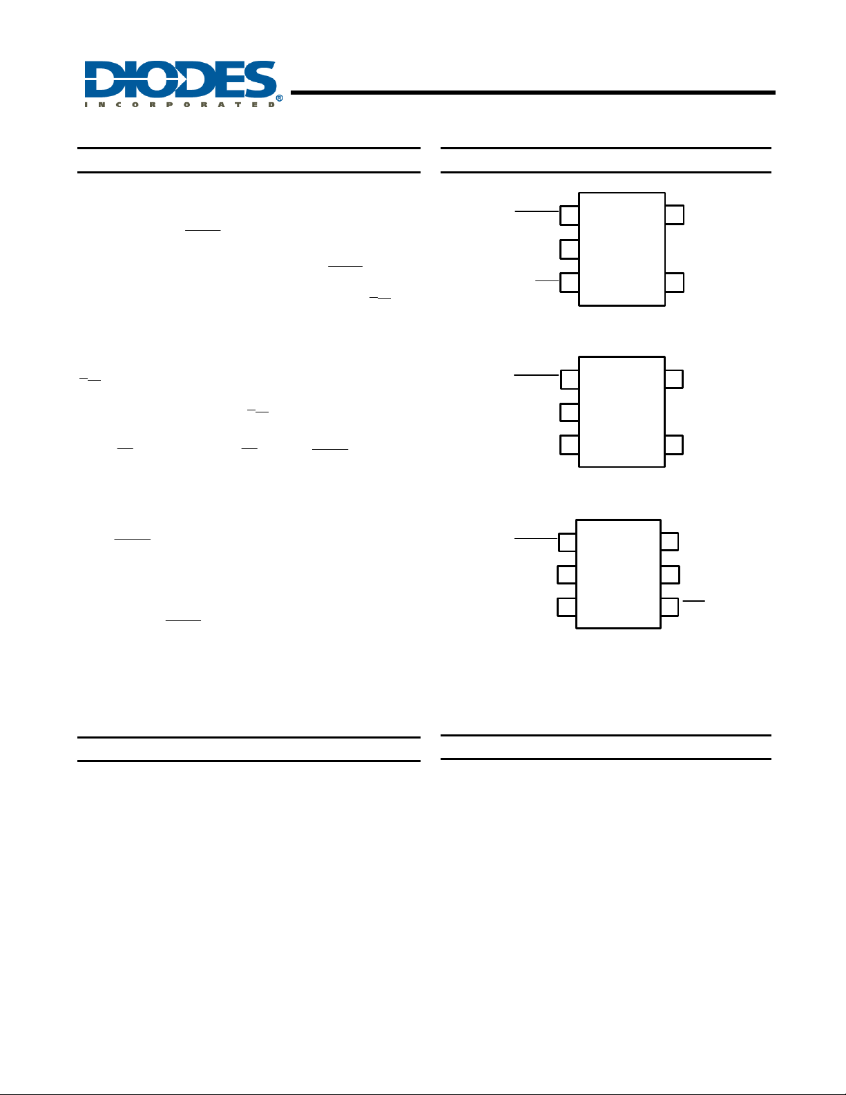
Pin Assignments
RESET
GND
MR
RESET
GND
RESET
RESET
GND
RESET
(Top View)
1
APX8 232
2
3 4
SOT25
(Top View)
1
2
2
APX824
3 4
SOT25
(Top View)
1
2
2
APX825A
3 4
SOT26
5
V
CC
WDI
5
V
CC
WDI
6
V
CC
5
WDI
MR
Applications
• Power-on reset generator with fixed delay time of 200ms
Typ
• Manual reset input (APX823/APX825A)
• Reset output available in active-low
(APX823/APX824/APX825A), active-high
(APX824/APX825A)
• Supply voltage supervision range 2.5V, 3V, 3.3V, 5V
• Watchdog timer
• Supply current of 30μA (Typ.)
• Temperature range: -40°C to 85°C
• SOT25 and SOT26: Available in “Green” Molding
Compound (No Br, Sb)
• Lead Free Finish/RoHS Compliant (Note 1)
Note: 1. EU Directive 2002/95/EC (RoHS). All applicable RoHS exemptions applied, see EU Directive 2002/95/EC Annex Notes.
• Applications Using DSPs, Microcontrollers, or
Microprocessors
• Industrial Equipment
• Programmable Controls
• Automotive Systems
• Portable/Battery-Powered Equipment
• Intelligent Instruments
• Wireless Communications Systems
• Notebook/Desktop Computers
APX823/APX824/APX825A
Document number: DS31323 Rev. 4 - 2
1 of 12
www.diodes.com
May 2011
© Diodes Incorporated

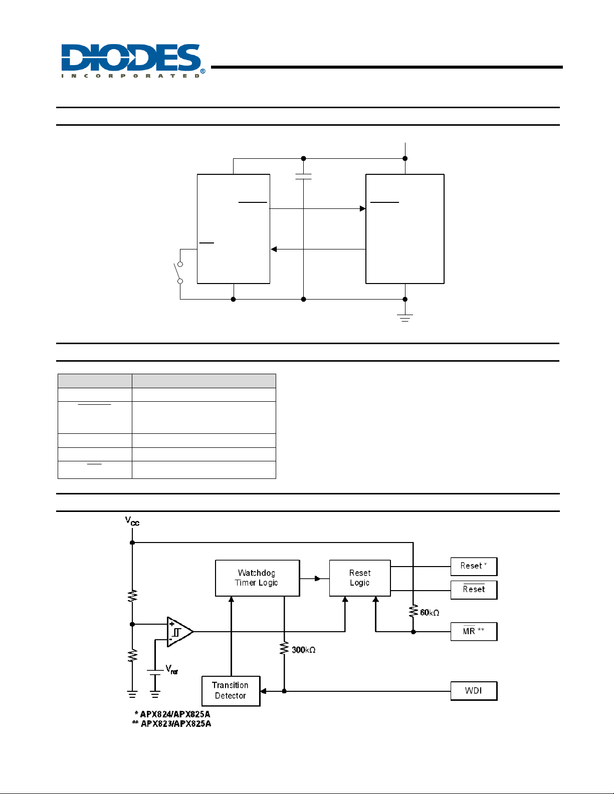
Typical Application Circuit
APX823/APX824/APX825A
PROCESSOR SUPERVISORY CIRCUITS
V
CC
C
IN
V
CC
100nF
V
CC
Pin Descriptions
Pin Name Description
GND Ground
RESET
(RESET)
Reset output pin
VCC
WDI Watchdog input
MR
Operating voltage input
Manual reset
Functional Block Diagram
RESET
APX8XX Microprocessor
MR WDI
GND
RESET
I/O
GND
APX823/APX824/APX825A
Document number: DS31323 Rev. 4 - 2
2 of 12
www.diodes.com
May 2011
© Diodes Incorporated

APX823/APX824/APX825A
×
Absolute Maximum Ratings (Over operating ambient temperature range, unless otherwise noted)*
Symbol Parameter Rating Unit
ESD HBM Human Body Model ESD Protection 5 KV
ESD MM Machine Model ESD Protection 200 V
VCC
V
RESET
ICC Input Current VCC
IO
PD
TOP
TST
* Stresses beyond those listed under “absolute maximum ratings” may cause permanent damage to the device. These are stress ratings only, and functional
operation of the device at these or any other conditions beyond those indicated under “recommended operating conditions” is no t implied. Exposure to absolute-
maximum-rated conditions for extended periods may affect device reliability.
Recommended Operating Conditions
Symbol Parameter Min Max Unit
VCC
VIN
VIH
VIL
Δt/ΔV
TA
TR VCC Rising Time (VCC = 0~VT)
Supply Voltage 6.0 V
RESET, RESET , MR , WDI
Maximum High Output Current 20 mA
Derating Factor Above
T
= 25oC
A
Continuous Total Power
Dissipation
Operating Junction Temperature Range -40 to 105 °C
Storage Temperature Range -65 to 150 °C
Supply Voltage 1.1 5.5 V
Input Voltage 0
High-level Input Voltage at
Low-level Voltage -
Input Transition Rise and Fall Rate at
Operating Ambient Temperature Range -40 85
TA = 25oC Power Rating
TA = 70oC Power Rating
TA = 85oC Power Rating
MR and WDI
MR or WDI
PROCESSOR SUPERVISORY CIRCUITS
-0.3 to (VCC+0.3)
20 mA
SOT25 6.2
SOT26 5.8
SOT25 500
SOT26 470
SOT25 220
SOT26 210
SOT25 125
SOT26 120
(VCC+0.3)
VCC
0.7
- 100 ns/V
- 100 V/ uS
- V
0.3×VCC
V
mW/°C
mW
mW
mW
V
V
o
C
APX823/APX824/APX825A
Document number: DS31323 Rev. 4 - 2
3 of 12
www.diodes.com
May 2011
© Diodes Incorporated

APX823/APX824/APX825A
×
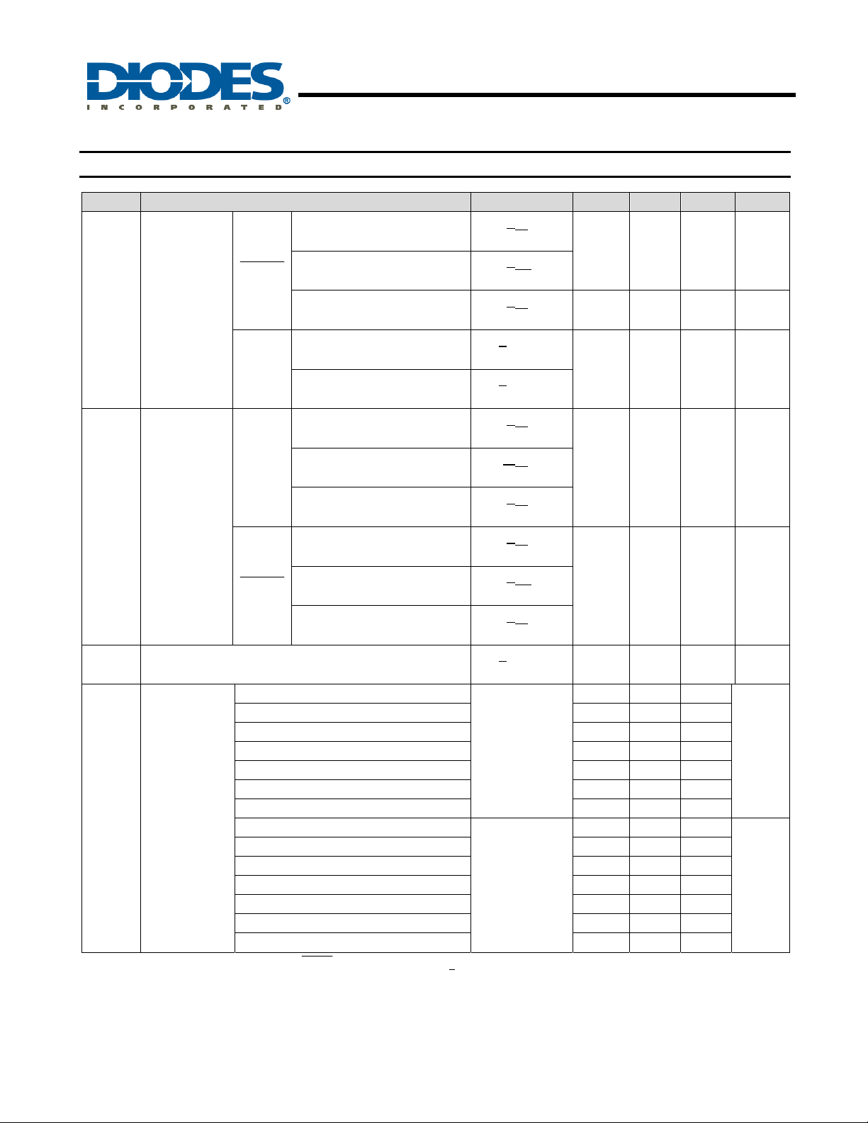
Electrical Characteristics (Over recommended operating ambient temperature range, unless otherwise noted)
Symbol Parameter Test Conditions Min Typ. Max Unit
APX823/APX824/APX825A 29/26/23
RESET
High-level
VOH
Output Voltage
RESET
RESET
Low-level
VOL
Output Voltage
RESET
V
RESET
Power-up Reset Voltage (see Note 2)
Negative-going
V
Input Threshold
TH-
Voltage
(see Note 3)
Note: 2. The lowest supply voltage at which
3. To ensure best stability of the threshold voltage, a bypass capacitor (ceramic, 0.1μF) should be placed near the supply terminals.
APX823/APX824/APX825A 40/31
APX823/APX824/APX825A
–46/44
APX824/APX825A
-29/26/23
APX824/APX825A -
46/44/40/31
APX824/APX825A
-29/26/23
APX824/APX825A -46/44
APX823/APX824/APX825A -
29/26/23
APX823/APX824/APX825A -
40/31
APX823/APX824/APX825A -
46/44
APX823/APX824/APX825A -23
APX823/APX824/APX825A -26 2.59 2.63 2.69
APX823/APX824/APX825A -29 2.88 2.93 3.00
APX823/APX824/APX825A -31 3.02 3.08 3.15
APX823/APX824/APX825A -40 3.93 4.00 4.08
APX823/APX824/APX825A -44 4.31 4.38 4.47
APX823/APX824/APX825A -46 4.56 4.63 4.72
APX823/APX824/APX825A -23
APX823/APX824/APX825A -26 2.57 2.63 2.69
APX823/APX824/APX825A -29 2.86 2.93 3.00
APX823/APX824/APX825A -31 3.00 3.08 3.15
APX823/APX824/APX825A -40 3.92 4.00 4.08
APX823/APX824/APX825A -44 4.29 4.38 4.47
APX823/APX824/APX825A -46 4.54 4.63 4.72
becomes active. TR , VCC > 15μs/V.
RESET
PROCESSOR SUPERVISORY CIRCUITS
= V
TH-
= V
TH-
= V
TH-
=-120μA
> 1.8V,
= -100μA
> 1.8V,
= -150μA
= V
TH-
=1mA
= V
TH-
=1.2mA
= V
TH-
TH-
= V
TH-
=1.2mA
= V
TH-
+0.2V
+0.2V
+0.2V
+0.2V
+0.2V
+0.2V
-0.2V
-0.2V
-0.2V
0.8×VCC
VCC-1.5V
VCC
0.8
- - V
- - V
- - V
- - 0.4 V APX824/APX825A -40/31
- - 0.4 V
- - 0.4 V
2.21 2.25 2.30
V
2.20 2.25 2.30
V
V
CC
IOH=-20μA
V
CC
IOH=-30μA
V
CC
I
OH
V
CC
I
OH
V
CC
I
OH
V
CC
I
OL
V
CC
I
OL
V
CC
IOL=3mA
VCC= V
IOL=1mA
V
CC
I
OL
V
CC
IOL=3mA
VCC > 1.1V,
IOL=20μA
= 0oC -85oC
T
A
= -40oC -85oC
T
A
APX823/APX824/APX825A
Document number: DS31323 Rev. 4 - 2
4 of 12
www.diodes.com
May 2011
© Diodes Incorporated
 Loading...