

Page 1
APX811/812
4-Pin Microprocessor Supervisor With Manual Reset
Features
• Precision Monitor of(2.5V/3.0V/3.3V/5.0V) power
supply voltage
• Full specified over temperature
• Manual reset input
• Available in four output configuration
• Push-pull
• Push-pull RESET Acti ve high(APX812)
• Power-on reset generator with fixed delay time 200ms
• SOT143: Available in “Green” Molding Compound
(No Br, Sb)
• Lead Free Finish/RoHS Compliant (Note 1)
Active low(APX811)
RESET
Applications
• Computers
• Controllers
• Intelligent Instruments
• Critical uP and UC power Monitoring
• Portable/Battery powered Equipment
• Automotive
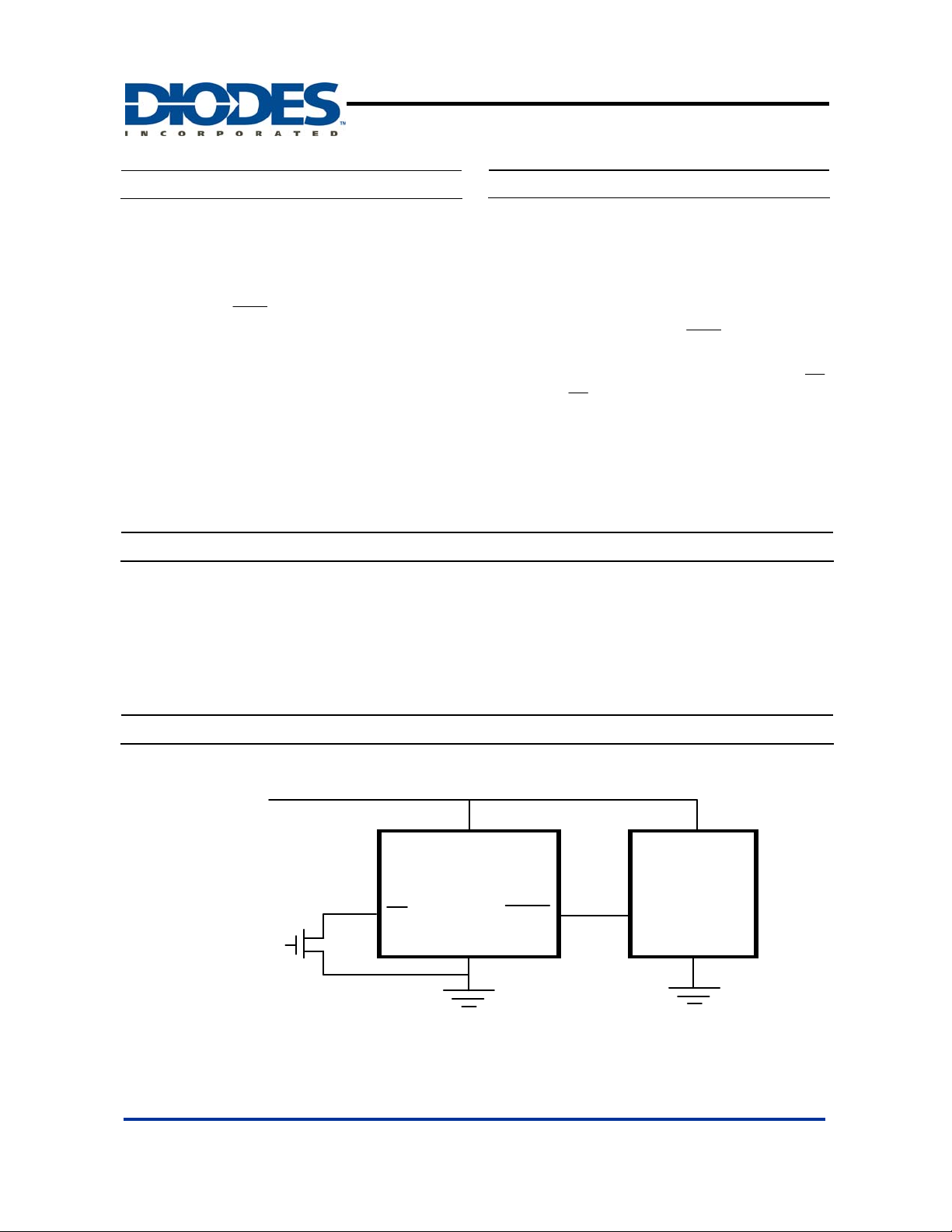
Typical Application Circuit
General Description
The APX811/812 are used for microprocessor supervisory circuit
to monitor the power supplies in These circuit perform a single
function: they assert a reset signal whenever the Vcc supply
voltage declines below a preset threshold, keeping it asserted for
at least 240ms after Vcc has risen above the reset threshold.
Reset thresholds suitable for operation with a variety of supply
voltages are available. The APX811/812 have push-pull outputs.
The APX811 has an active low
APX812 has an active high RESET output.
The APX811/812 devices incorporate a manual reset input,
A low level at
The APX811/2 are t argeted at 2.5V, 3V, 3.3V a nd 5V powered
systems and are available with different threshold voltages to
meet the exact needs of the system. They ar e available in the
space saving SOT143 package and operate over the whole
industrial temperature range, -40 to 85°C.
causes RESET to become active.
MR
output, while the
RESET
MR
.
Vcc
(Manual Reset)
Push Botton
Vcc
APX811/APX812
MR
GND
RESET
(RESET)
Vcc
MCU
RESET Input
GND
APX811/812 Rev. 2 1 of 10 OCTOBER 2009
DS31960 www.diodes.com © Diodes Incorporated
Page 2
Ordering Information
APX811/812
4-Pin Microprocessor Supervisor With Manual Reset
APX 8 XX - XX U G - 7
Enable
11 : Active-Low
12 : Active-High
Voltage
46 : 4.63
44 : 4.38
40 : 4.00
31 : 3.08
29 : 2.93
26 : 2.63
23 : 2.25
Package
U : SOT143
Green
G : Green
Packing
7 : Tape & Reel
Device
APX811-XXUG-7 U SOT143 3000/Tape & Reel -7
APX812-XXUG-7 U SOT143 3000/Tape & Reel -7
Notes: 1. EU Directive 2002/95/EC (RoHS). All applicable RoHS exemptions applied. Pl ease visit our website at
http://www.diodes.com/datasheets/ap02001.pdf
http://www.diodes.com/products/lead_free.html
2. Pad layout as shown on Diodes Inc. suggested pad layout document AP02001, which can be found on our website at
Package
Code
Packaging
(Note 2)
.
.
Quantity Part Number Suffix
7” Tape and Reel
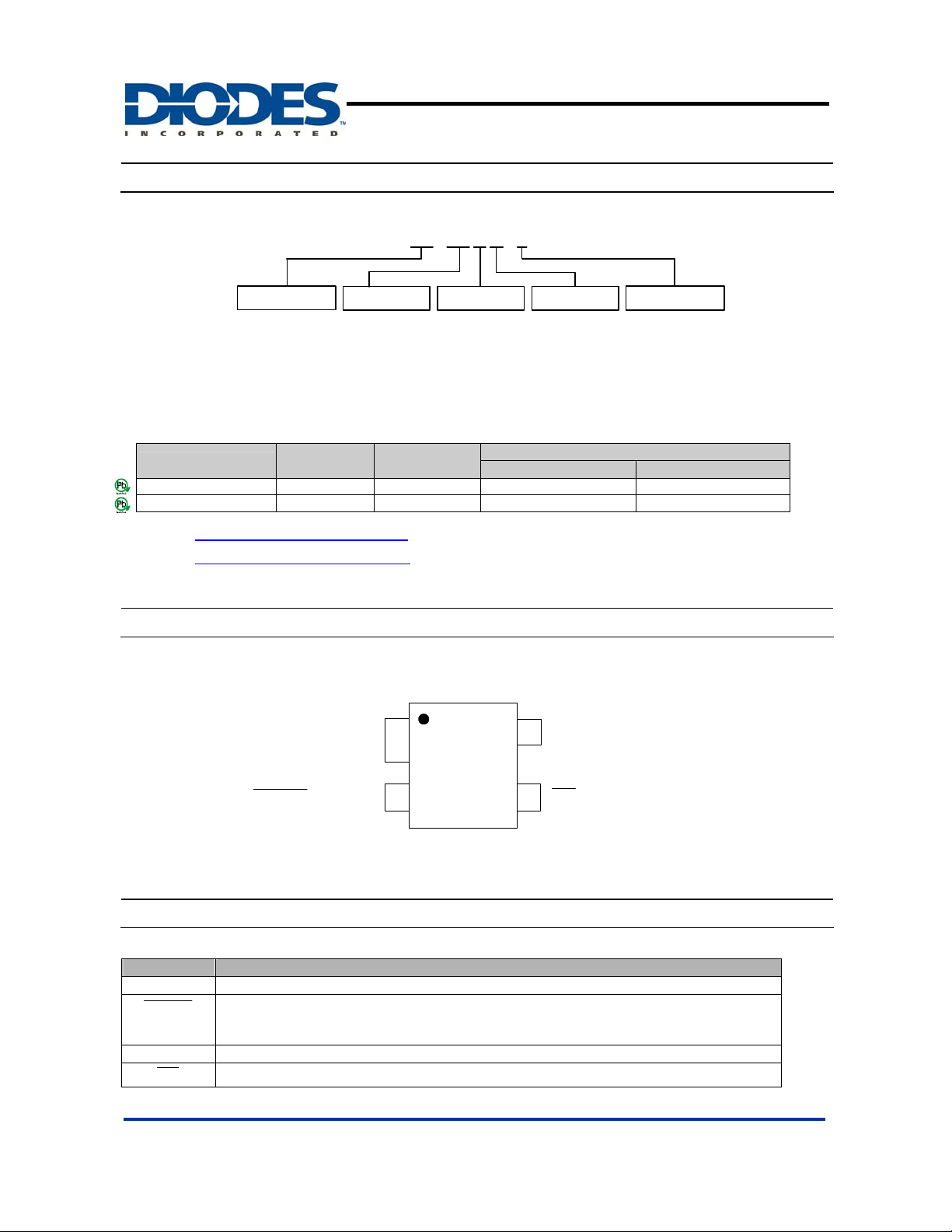
Pin Assignments
( Top View )
4
GND
1
Vcc
MR
3
RESET
(RESET)
2
SOT143
Pin Descriptions
Pin Name Description
GND Ground
RESET
(RESET)
VCC Operating Voltage Input
MR
APX811/812 Rev. 2 2 of 10 OCTOBER 2009
DS31960 www.diodes.com © Diodes Incorporated
Reset output Pin
L: for APX811
H: for APX812
Manual reset (Active Low)
Page 3
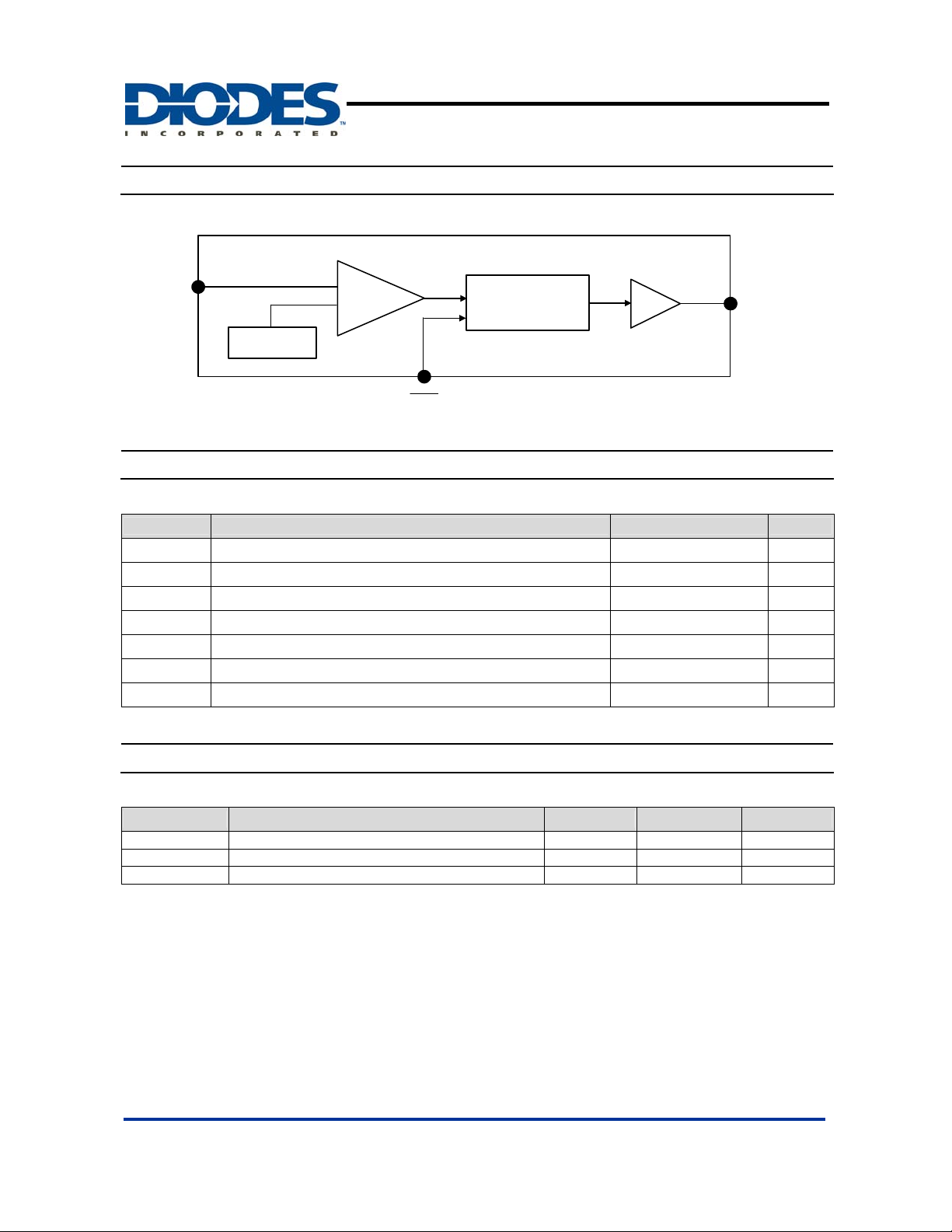
Block Diagram
APX811/812
4-Pin Microprocessor Supervisor With Manual Reset
Vcc
Delay Circuit
Driver
RESET
Vref
MR
Absolute Maximum Ratings
Symbol Parameter Rating Unit
ESD HBM Human Body Model ESD protection 3 kV
ESD MM Machine Model ESD Protection 500 V
VCC Supply voltage -0.3~7 V
V
RESET -0.3 to (Vcc+0.3) V
RESET
ICC Input Current, Vcc 20 mA
IO Output current 20 mA
PD Power dissipation 320 mW
Recommended Operating Conditions
Symbol Parameter Min Max Unit
VCC Supply Voltage 1.1 5.5 V
VIN Input Voltage 0 (VCC+0.3) V
TA Operating Ambient Temperature -40 85
APX811/812 Rev. 2 3 of 10 OCTOBER 2009
DS31960 www.diodes.com © Diodes Incorporated
o
C
Page 4

T
APX811/812
4-Pin Microprocessor Supervisor With Manual Reset
Electrical Characteristics (T
= 25ºC)
A
T
= -40 to 85
A
o
C unless otherwise note. Typical values are at TA=+25 oC.
Symbol Parameter Test Conditions Min Typ. Max Unit
VCC V
ICC Supply Current
Range 1.0 5.5 V
CC
V
th
+ 0.2V
30 40 µA
2.22 2.25 2.28 V
2.59 2.63 2.67 V
2.89 2.93 2.98 V
Reset threshold T
Vth
=25
A
o
C.
3.03 3.08 3.13 V
3.94 4.00 4.06 V
4.31 4.38 4.45 V
4.56 4.63 4.70 V
Set-up Time
t
s
VOL
VOH
VOL
V
OH
θ
JA
θ
JC
Notes: 3. Test condition for SOT143: Device mounted on FR-4 substrate, 1"*1", 2oz, copper, single-sided, PC boards.
TRESE Output Vol tage Low
(APX811)
Output Voltage-High
TRESE
(APX811)
RESET Output Voltage-Low
(APX812)
RESET Output Voltage-High
(APX812)
Thermal Resistance
Junction-to-Ambient
hermal Resistance
Junction-to-Case
V
= Vth to (Vth – 100mV)
CC
V
= V
CC
V
= V
CC
V
> 1.0V, I
CC
V
> V
CC
I
SOURCE
V
> V
CC
I
SOURCE
V
= V
CC
V
= V
CC
-0.2, I
th
-0.2, I
th
+0.2,
th
= 500uA
+0.2,
th
= 800uA
+0.2, I
th
+0.2, I
th
= 1.2mA
SINK
= 3.2mA
SINK
= 50uA 0.3
SINK
= 1.2mA
SINK
= 3.2mA
SINK
1.8V < VCC < Vth -0.2,
I
= 150uA
SOURCE
SOT143 (Note 3) 240
SOT143 (Note 3) 71
20 µs
0.3
0.4
0.8V
CC
V
V
V
–1.5
CC
0.3
0.4
0.8 V
CC
V
V
o
C/W
o
C/W
Timing requirements (T
=25oC)
A
Symbol Parameter Test Conditions Min Typ. Max Unit
tW Pulse Width
at
MR
> V
V
CC
+0.2V, VIL=0.3×VCC, VIH=0.7×VCC
th-
100 - - ns
APX811/812 Rev. 2 4 of 10 OCTOBER 2009
DS31960 www.diodes.com © Diodes Incorporated
Page 5

APX811/812
4-Pin Microprocessor Supervisor With Manual Reset
Switching Characteristics (T
=25oC)
A
Symbol Parameter Test Conditions Min Typ. Max Unit
V
> V
+0.2V,
th-
> V
+0.2V,
th-
=0.3×VCC,
=0.7×VCC
= V
-0.2V,
th-
= V
+0.2V
th-
> V
+0.2V,
th-
=0.3×VCC,
=0.7×VCC
= V
-0.2V,
th-
= V
+0.2V
th-
140 200 280 ms
- - 0.1 µs
- - 25 µs
- - 0.1 µs
- - 25 µs
t
t
Delay Time APX811/812
t
d
Propagation (Delay) Time,
PHL
High-to-low-level Output
Propagation (Delay) Time,
PLH
Low-to-high-level Output
MR
to
RESET
delay (APX811/812)
to RESET delay
V
CC
MR to RESET delay
(APX811/812)
V
to RESET delay
CC
(APX811/812)
CC
See timing diagram
V
CC
V
IL
V
IH
V
IL
V
IH
V
CC
V
IL
V
IH
V
IL
V
IH
Timing Diagram
RESET vs. Vcc Timing Diagram
Vcc
/RESET
RESET
/RESET
Vcc
/MR
Vth
Vth
Vth
Vth
d
t
td
td
td
RESET vs. /MR Timing Diagram
td
td
APX811/812 Rev. 2 5 of 10 OCTOBER 2009
DS31960 www.diodes.com © Diodes Incorporated
Page 6

)
)
)
)
4-Pin Microprocessor Supervisor With Manual Reset
Typical Performance Characteristics
APX811/812
RESE T Timeout Period v s. Temperature
250
240
230
220
210
200
190
180
170
160
RESET Timeout Period (ms
150
-40℃ -25℃ 0℃ 25℃ 50℃ 85℃ 105℃ 125℃
Temperature
RE SE T Threshold Voltage vs. Temperature
3.2
3.15
3.1
3.05
3
2.95
2.9
2.85
RESET Thershold Vo l tage (V
2.8
-40℃ -25℃ 0℃ 25℃ 50℃ 85℃ 105℃ 125℃
Temperature
Vcc Supp ly Curren t vs. Temp er at ure
(Vcc=3.3V Vth = 2. 93V )
35
34
33
32
31
30
29
28
27
Vcc Supply Current (µA
26
25
-40℃ -25℃ 0℃ 25℃ 50℃ 85℃ 105℃ 125℃
Temperature
Supply Curreny vs. Vcc
40
35
30
25
20
15
10
Supply Current (µA
5
0
1.5V 2.5V 3.3V 4.0V 5.0V 5.5V
Vcc
APX811/812 Rev. 2 6 of 10 OCTOBER 2009
DS31960 www.diodes.com © Diodes Incorporated
Page 7

APX811/812
4-Pin Microprocessor Supervisor With Manual Reset
Application Information
A microprocessor’s (µP’s) reset input starts the µP in a known state. The APX811/812 asserts reset to prevent code-execution errors
during power-up, power-down, or brownout conditions. They assert a reset signal whenever the V
preset threshold or the
APX811/812 have a push-pull output stage.
The APX811/812 reset output is guaranteed to be logic low for the APX811 and high the APX812 for V
reset threshold, an internal timer keeps
interval, the APX811’s
reset threshold), the APX811’s
threshold, the internal timer resets to zero, and
the reset threshold, and
Ensuring a Valid Reset Output Down to V
When V
CMOS logic inputs connected to
µP and other circuit ry is i nop er ativ e with V
down resistor to
large enough not to load
For the APX812 if RESET is required to remain valid for V
recommended.
Benefits of Highly Accurate Reset Threshold
Most µP supervisor ICs has reset threshold vol tages between 5% and 10% below the value of nominal supply voltages. This ensures a
reset will not occur within 5% of the nominal supply, but will occur when the supply is 10% below nominal. When using ICs rated at only
the nominal supply ±5%, this leaves a zone of unce rtainty where the supply is be tween 5% a nd 10% low, and w here the reset may or may
not be asserted.
falls below 1V, the APX811
CC
RESET
pin is brought low, keeping it asserted for at least 240ms after VCC has risen above the reset threshold. The
MR
output low (and R ESET high for the APX812) for the reset timeout period. After this
RESET
output goes high (APX812’s RESET output goes low). If a brownout condition occurs (VCC dips below the
RESET
output goes low (APX812’s RESET output goes high). Any time VCC goes below the reset
RESET
goes low (RESET goes high). The internal timer starts after VCC returns above
RESET
remains low (RESET remains high) for the reset timeout period.
RESET
= 0
CC
no longer sinks current-— it becomes an open circuit. Therefore, high-impedance
RESET
can drift to undetermined voltages. This presents no problem in most applications since most
RESET
below 1V. However, in applications where
CC
causes any stray leakage currents to flow to ground, holding
and small enough to pull
RESET
to ground.
RESET
< 1V then a 100kΩ pull-up resistor between RESET and VCC is
CC
RESET
RESET
APX811/812 Rev. 2 7 of 10 OCTOBER 2009
DS31960 www.diodes.com © Diodes Incorporated
supply voltage declines below a
CC
> 1V. Once VCC exceeds the
CC
must be valid down to 0V, ad di ng a pul l
low. R1’s value is not critical; 100k is
Page 8

Marking Information
(1) SOT143
( Top View )
APX811/812
4-Pin Microprocessor Supervisor With Manual Reset
Y W
3
XX : Identification code
: Year 0~9
Y
: Week : A~Z : 1~26 week;
X
W
a~z : 27~52 week; z represents
4
XX
52 and 53 week
: A~Z : Green
1 2
Device Package Identification Code
APX811-46U SOT143 C2
APX811-44U SOT143 C3
APX811-40U SOT143 C4
APX811-31U SOT143 C5
APX811-29U SOT143 C6
APX811-26U SOT143 C7
APX811-23U SOT143 C8
APX812-46U SOT143 C9
APX812-44U SOT143 CA
APX812-40U SOT143 CB
APX812-31U SOT143 CC
APX812-29U SOT143 CD
APX812-26U SOT143 CE
APX812-23U SOT143 CF
APX811/812 Rev. 2 8 of 10 OCTOBER 2009
DS31960 www.diodes.com © Diodes Incorporated
X
Page 9

4-Pin Microprocessor Supervisor With Manual Reset
Package Information (All Dimensions in mm)
(1) Package Type: SOT143
APX811/812
0.77/0.93
1.78/2.03
1.58/1.83
2.80/3.0
0.37/0.51
0.45/0.6
2.28/2.48
1.20/1.40
0.085/0.18
0.89/1.0
0.013/0.10
0.46/0.6
.
p
y
t
°
8
APX811/812 Rev. 2 9 of 10 OCTOBER 2009
DS31960 www.diodes.com © Diodes Incorporated
Page 10

APX811/812
4-Pin Microprocessor Supervisor With Manual Reset
DIODES INCORPORATED MAKES NO WARRANTY OF ANY KIND, EXPRESS OR IMPLIED, WITH REGARDS TO THIS
DOCUMENT, INCLUDING, BUT NOT LIMITED TO, THE IMPLIED WARRANTIES OF MERCHANTABILITY AND FITNESS FOR A
PARTICULAR PURPOSE (AND THEIR EQUIVALENTS UNDER THE LAWS OF ANY JURISDICTION).
Diodes Incorporated and its subs idiaries reserve the right to make modific ations, enhancem ents, improvem ents, correctio ns or other
changes without further notic e to this document and any product des cri bed herein. Diodes Inc orporat ed does not assum e any liabi lity
arising out of the applicati on or use of this document or any produc t described herein ; neither does Diodes In corporat ed convey any
license under its patent or trademark rights, nor the rights of others . Any Customer or user of t his document or produc ts described
herein in such applicati ons shall assume all risks of such use and will agree to hold Diodes Incorporated and all the companies
whose products are represented on Diodes Incorporated website, harmless against all damages.
Diodes Incorporated do es not warrant or accept an y liabilit y whatsoever in re spect of any product s purchased through unaut horized
sales channel.
Should Customers purchase or use Diod es Incorporated products for any unintend ed or unauthorized application, Custom ers shall
indemnify and hold Diodes Incorpor ated and its repres entatives harmless agai nst all claims, damages , expenses, and atto rney fees
arising out of, directly or indi re ct l y, any c l a im of person al i nj u ry or death ass oci a t e d with suc h uni nte nde d or un authorized application.
Products described h erein may be covered by one or more United States, i nternational or f oreign patents pendi ng. Product names
and markings noted herein may also be covered by one or more Uni ted S tates, international or foreign trademarks.
Diodes Incorporated products are specific ally not authorized for use as critical components in life support devic es or systems without
the express written approval of t he Chief Execut ive Officer of Diodes Incorporated. As used herein:
A. Life support devices or systems are devices or systems which:
1. are i nte nde d t o imp l ant i nto the body, or
2. support or sustain life and whose failure to perform when properly used in accordance with instructions for us e provided
in the labeling can be reasonably expected to result in significant injury to the user.
B. A critica l component is an y component in a l ife support devi ce or system whose failure t o perform can be reas onably expecte d
to cause the failure of the life support device or to affect its safety or effectiveness.
Customers represent that they have all nec essary expertise in the safet y and regulatory ramificati ons of their life support devices or
systems, and acknowledge and agree that they are solely responsible for all legal, regulatory and safety-related requirements
concerning their products and any use of Diodes Incorporated products in such safety-critical, life support devices or systems,
notwithstanding any devices- or systems-related information or support that may be provided by Diodes Incorporated. Further,
Customers must fully indemnif y Diodes Incorporated and its representati ves against any damages arising out of the use of Diodes
Incorporated products in such safety-critical, life support devices or systems.
Copyright © 2009, Diodes Incorporated
www.diodes.com
IMPORTANT NOTICE
LIFE SUPPORT
APX811/812 Rev. 2 10 of 10 OCTOBER 2009
DS31960 www.diodes.com © Diodes Incorporated
 Loading...