Diodes APX809, APX810 User Manual

APX809/810
3-PIN MICROPROCESSOR RESET CIRCUITS
Features
• Precision Monitoring of +2.5V, +3V, +3.3V, and +5V
Power-Supply Voltages
• Fully Specified Over Temperature
• Available in three Output Configurations
• Push-Pull
• Push-Pull
• 200ms Typ Power-On Reset Pulse Width
• 30µA Supply Current (Typ.)
• Guaranteed Reset Valid to V
• No External Components
• SOT23 and SOT23R: Available in “Green” Molding
Compound (No Br, Sb)
• Lead Free Finish/RoHS Compliant (Note 1)
RESET Active Low (APX809)
RESET Active High (APX810)
= +1V
CC
Applications
• Computers
• Controllers
• Intelligent Instruments
• Critical µP and µC Power Monitoring
• Portable/Battery Powered Equipment
• Automotive
Ordering Information
General Description
The APX809/810 are used for microprocessor (µP) supervisory
circuits to monitor th e power supplies in µP and digital systems .
They provide excellent circuit reliability and low cost by
eliminating external components and adjustments when used
with +5V, +3.3V, +3.0V powered circuits.
These circuits perform a single function: they assert a reset
signal whenever the V
threshold, keeping it asserted for at least 240ms after V
risen above the reset threshold. Reset thresholds suitable for
operation with a variety of supply voltages are available. The
APX809/810 have push pull outputs. The APX809 have an active
low
RESET
RESET output. The reset comparator is designed to ignore fast
transients on V
correct logic state for V
the APX809/810 ideal for use in portable equipment. The
APX809/810 is available in a 3-pin SOT23 and SOT23R
packages.
output, while the APX810 has an active high
CC
supply voltage declines below a preset
CC
, and the outputs are guaranteed to be in the
down to 1V. Low supply current makes
CC
CC
has
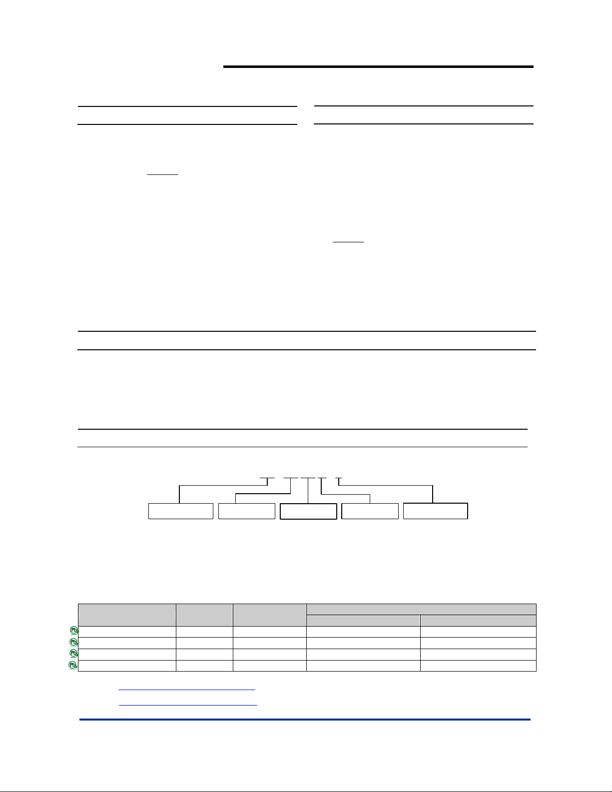
APX 8 XX - XX XX G - 7
Enable
09 : Active-Low
10 : Active-High
Voltage
46 : 4.63
44 : 4.38
Package
SA : SOT23
SR : SOT23R
40 : 4.00
31 : 3.08
29 : 2.93
26 : 2.63
23 : 2.25
Device
Package
Code
Packaging
(Note 2)
APX809-XXSAG-7 SA SOT23 3000/Tape & Reel -7
APX810-XXSAG-7 SA SOT23 3000/Tape & Reel -7
APX809-XXSRG-7 SR SOT23R 3000/Tape & Reel -7
APX810-XXSRG-7 SR SOT23R 3000/Tape & Reel -7
Notes: 1. EU Directive 2002/95/EC (RoHS). All applicable RoHS exemptions applied. Please visit our website at
http://www.diodes.com/products/lead_free.html
2. Pad layout as shown on Diodes Inc. suggested pad layout document AP02001, which can be found on our website at
http://www.diodes.com/datasheets/ap02001.pdf
.
.
APX809/810 Rev. 4 1 of 9 FEBRUARY 2009
www.diodes.com © Diodes Incorporated
Green
G : Green
Packing
7 : Tape & Reel
7” Tape and Reel
Quantity Part Number Suffix

Pin Assignments
APX809/810
3-PIN MICROPROCESSOR RESET CIRCUITS
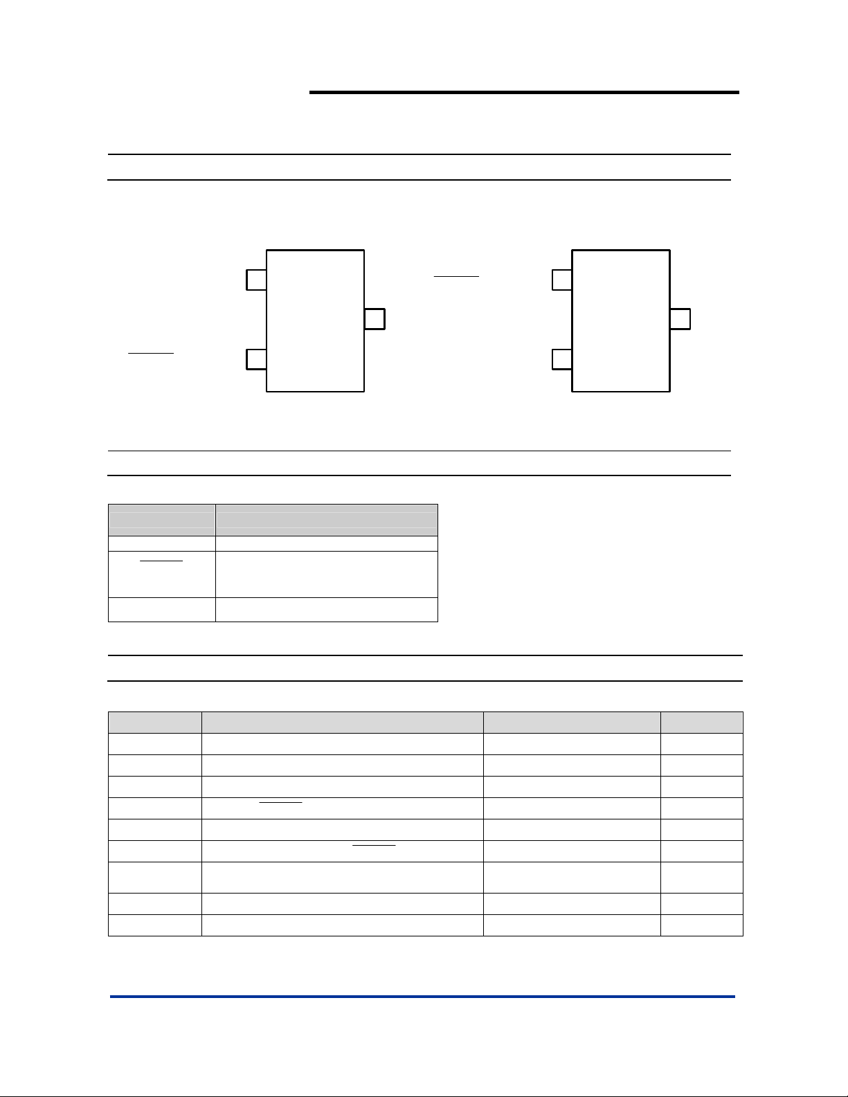
( Top View )
( Top View )
1
2
2
APX809
APX810
3
V
CC
RESET
GND
(RESET)
1
2
2
APX809
APX810
RESET
3
V
CC
(RESET)
GND
SOT23RSOT23
Pin Descriptions
Pin Name Description
GND Ground
RESET
(RESET)
VCC Operating Voltage Input
Reset Output Pin
L: for APX809
H: for APX810
Absolute Maximum Ratings
Symbol Parameter Rating Unit
ESD HBM Human Body Model ESD Protection 5 KV
ESD MM Machine Model ESD Protection 500 V
VCC Supply Voltage -0.3 to +6.0 V
V
RESET
ICC Input Current, VCC 20 mA
IO
PD
TOP Operating Junction Temperature Range -40 to +105 °C
TST Storage Temperature Range -65 to +150 °C
APX809/810 Rev. 4 2 of 9 FEBRUARY 2009
RESET,
Output Current, RESET,
Continuous Power Dissipation (T
de-rate 4mW/°C above +70°C
RESET (push-pull)
RESET
www.diodes.com © Diodes Incorporated
= +70°C),
A
-0.3 to (V
+ 0.3) V
CC
20 mA
400 mW

T
APX809/810
3-PIN MICROPROCESSOR RESET CIRCUITS
Recommended Operating Conditions
Symbol Parameter Min Max Unit
VCC Supply Voltage 1.1 5.5 V
VIN Input Voltage 0 (VCC+0.3) V
TA Operating Ambi ent Temperature Range -40 85
TR Vcc Rising Time (Vcc = 0~VT) 100 V/ uS
Electrical Characteristics (T
= 25ºC)
A
T
= -40 to 85
A
o
C unless otherwise note . Typical values are at TA=+25 oC.
Symbol Parameter Test Conditions Min Typ. Max Unit
VCC V
Range TA = 0oC to +70oC 1.0 5.5 V
CC
ICC Supply Current VTH+ 0.2V 30 40 μA
APX809/810-23
2.21 2.25 2.30
APX809/810-26 2.59 2.63 2.69
APX809/810-29 2.88 2.93 3.00
APX809/810-31 3.02 3.08 3.15
= 0oC-85oC
T
A
APX809/810-40 3.93 4.00 4.08
APX809/810-44 4.31 4.38 4.47
APX809/810-46 4.56 4.63 4.72
APX809/810-23
2.20 2.25 2.30
VTH
Reset
Threshold
APX809/810-26 2.57 2.63 2.69
APX809/810-29 2.86 2.93 3.00
T
APX809/810-31 3.00 3.08 3.15
= -40oC-85oC
A
APX809/810-40 3.92 4.00 4.08
APX809/810-44 4.29 4.38 4.47
APX809/810-46 4.54 4.63 4.72
Reset Threshold Tempco 30 ppm/ oC
TS Set-up Time V
T
Reset Active Timeout Period TA = 0oC to +85oC 140 200 280 ms
DELAY
VOL
VOH
VOL
V
OH
θ
JA
θ
JC
Notes: 3. Test condition for SOT23/ SOT23R: Devices mounted on FR-4 substrate PC board, 2oz copper, with minimum recommended pad layout.
TRESE Output Voltag e Lo w
(APX809)
Output Voltage-High
TRESE
(APX809)
RESET Output V oltage-Low
(APX810)
RESET Output Voltage-High
(APX810)
Thermal Resistance
Junction-to-Ambient
hermal Resistance
Junction-to-Case
= VTH to (VTH – 100mV) 20 μs
CC
V
= V
CC
V
CC
V
CC
V
CC
I
SOURCE
V
CC
I
SOURCE
V
CC
V
CC
-0.2, I
TH
= V
-0.2, I
TH
> 1.0V, I
> V
+0.2,
TH
= 500uA
> V
+0.2,
TH
= 800uA
= V
+0.2, I
TH
= V
+0.2, I
TH
1.8V < VCC < VTH -0.2,
I
= 150uA
SOURCE
= 1.2mA 0.3
SINK
= 3.2mA 0.4
SINK
= 50uA 0.3
SINK
0.8V
CC
–1.5
V
CC
= 1.2mA 0.3
SINK
= 3.2mA 0.4
SINK
0.8 V
V
CC
SOT23/SOT23R (Note 3) 201
SOT23/SOT23R (Note 3) 56
APX809/810 Rev. 4 3 of 9 FEBRUARY 2009
www.diodes.com © Diodes Incorporated
o
C
V
o
o
V
V
V
V
C/W
C/W
 Loading...