

Page 1
APX803/D
3-PIN MICROPROCESSOR RESET CIRCUIT
Description
The APX803/D is used for microprocessor (µP) supervisory
circuits to monitor the power supplies in µP and digital
systems. They provide excellent circuit reliability and low cost
by eliminating external components and adjustments when
used with +5V, +3.3V, +3.0V powered circuits.
These circuits perform a single function: they assert a reset
signal on power up and whenever the V
declines below a preset threshold, keeping it asserted for a
fixed period of time after V
threshold. For the APX803D this period is a minimum of 1ms
while for other APX803 variants it is at least 140ms. The reset
comparator is designed to ignore fast transients on V
the outputs are guaranteed to be in the correct logic state for
V
down to 1V.
CC
The APX803 is available with different reset thresholds
suitable for operation with a variety of supply voltages,
however the APX803D is available with a 2.93V threshold
voltage.
The APX803/D have an open collector active low
output and compliment Diodes APX809/10 which have pushpull output stages.. Low supply current makes the APX803/D
ideal for use in portable equipment. The APX803/D are
available in two pin out variants of the 3-pin SOT23 package.
has risen above the reset
CC
supply voltage
CC
, and
CC
RESET
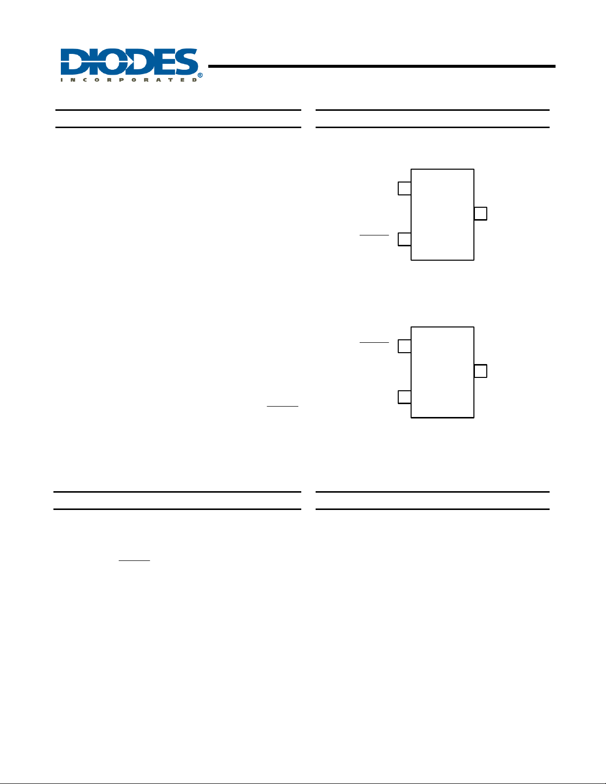
Pin Assignments
GND
RESET
RESET
GND
1
2
2
1
2
2
( Top View )
APX803
SOT23
( Top View )
APX803
SOT23R
3
V
CC
3
V
CC
Features
• Precision Monitoring of +2.5V, +3V, +3.3V, and +5V
Power-Supply Voltages
• Fully Specified Over Temperature
• Open-drain
• Power-On/power supply glitch Reset Pulse
• APX803D 2ms (Typ)
• APX803 200ms (Typ)
• 30µA Supply Current (Typ.)
• Guaranteed Reset Valid to VCC = +1V
• No External Components
• SOT23 and SOT23R: Available in “Green” Molding
Compound (No Br, Sb)
• Lead Free Finish/ RoHS Compliant (Note 1)
Notes: 1. EU Directive 2002/95/EC (RoHS). All applicable RoHS exemptions applied. Please visit our website at
RESET
http://www.diodes.com/products/lead_free.html.
APX803
Document number: DS32132 Rev. 2 - 2
Active Low
www.diodes.com
Applications
• Computers
• Controllers
• Intelligent Instruments
• Critical µP and µC Power Monitoring
• Portable/Battery Powered Equipment
1 of 11
September 2010
© Diodes Incorporated
Page 2
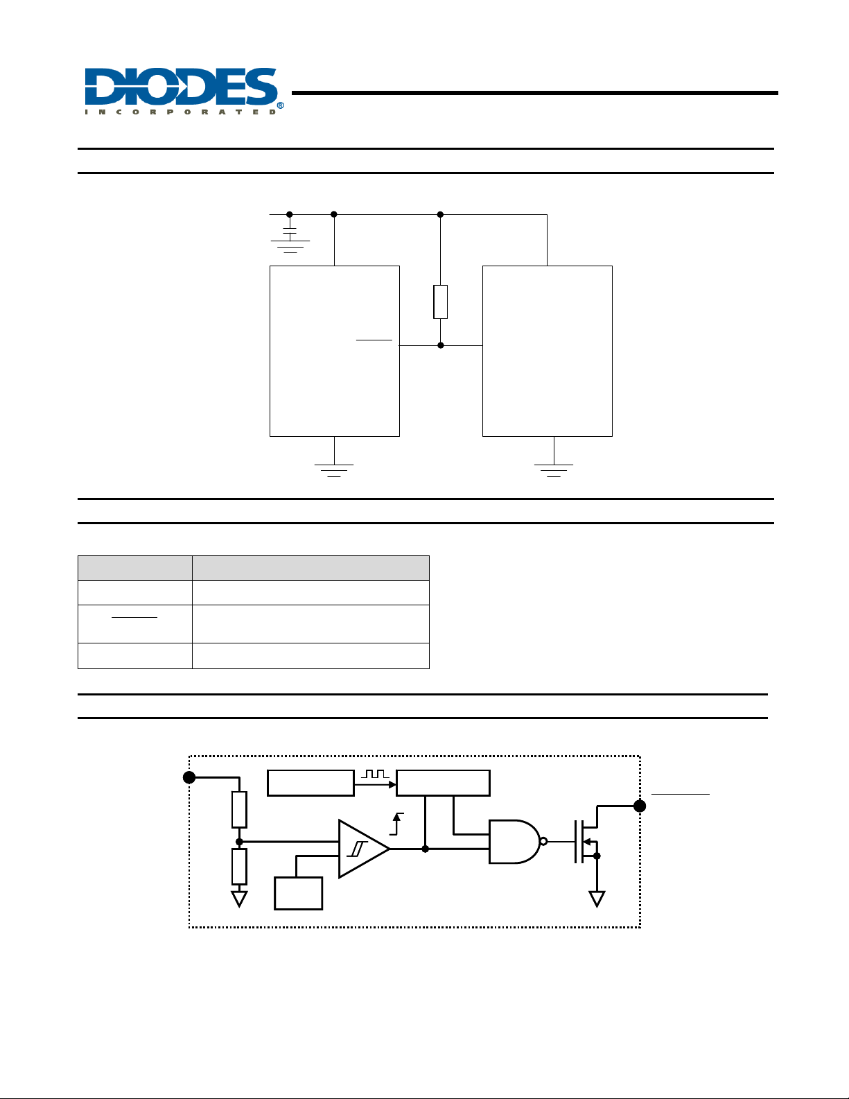
Typical Application Circuit
C
IN
100nF
APX803/D
3-PIN MICROPROCESSOR RESET CIRCUIT
V
CC
Pin Descriptions
Pin Name Description
GND Ground
Reset Output Pin
RESET
Active Low Open Drain
VCC Operating Voltage Input
V
CC
APX803
GND
RESET
V
CC
Microprocessor
RESET
INPUT
GND
Functional Block Diagram
V
V
CC
CC
APX803
Document number: DS32132 Rev. 2 - 2
V
V
REF
REF
Delay timeOscillator
Delay timeOscillator
APX803/D
APX803/D
2 of 11
www.diodes.com
RESET
RESETRESET
September 2010
© Diodes Incorporated
Page 3
APX803/D
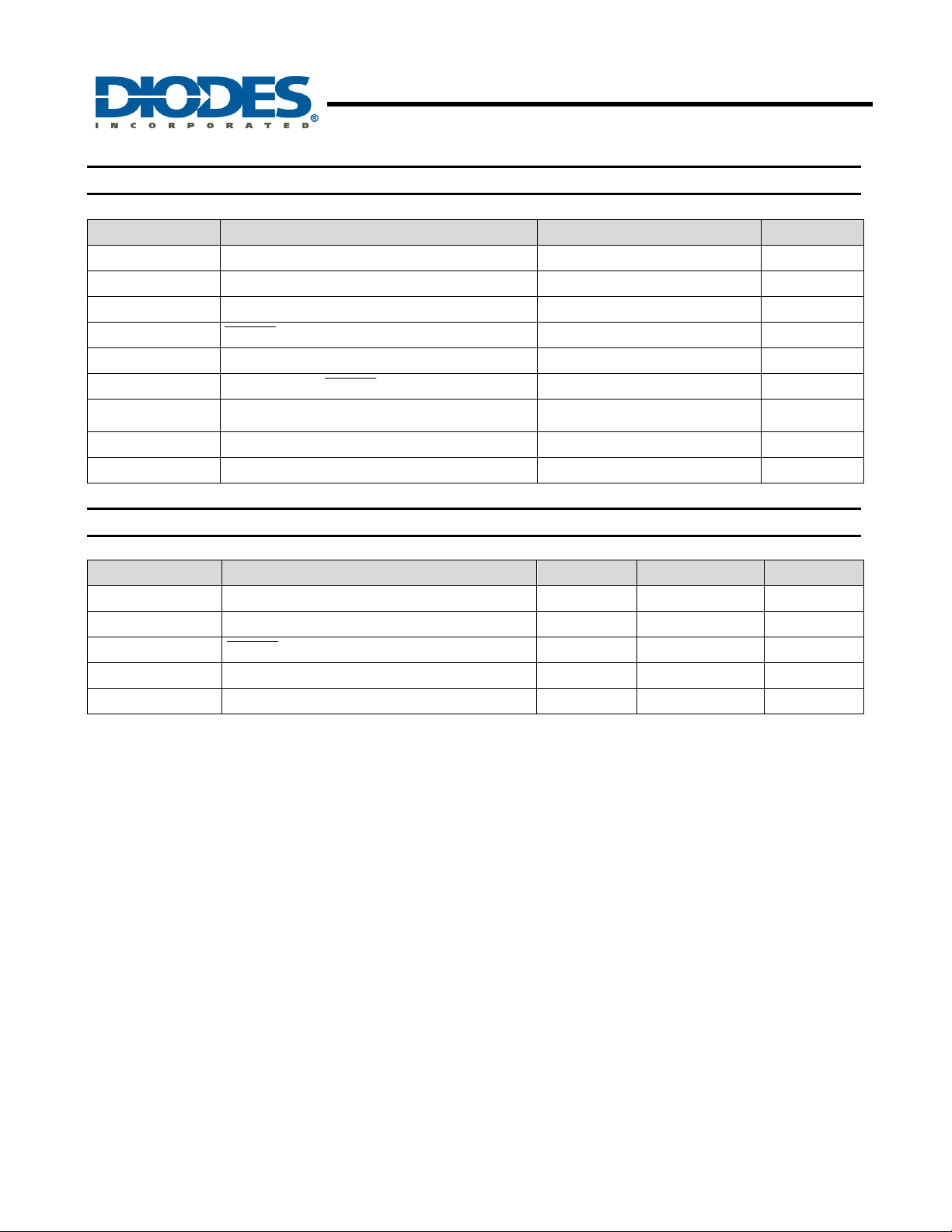
Absolute Maximum Ratings
Symbol Parameter Rating Unit
ESD HBM Human Body Model ESD Protection 2 kV
ESD MM Machine Model ESD Protection 200 V
VCC Supply Voltage -0.3 to +6.0 V
V
RESET
ICC Input Current, VCC 20 mA
IO
PD
TOP Operating Junction Temperature Range -40 to +105 °C
TST Storage Temperature Range -65 to +150 °C
Recommended Operating Conditions
RESET (open drain)
Output Current,
Continuous Power Dissipation (T
rate 4mW/°C above +70°C
RESET
= +70°C), de-
A
3-PIN MICROPROCESSOR RESET CIRCUIT
-0.3 to 6 V
20 mA
400 mW
Symbol Parameter Min Max Unit
VCC Supply Voltage 1.1 5.5 V
VIN Input Voltage 0 (VCC+0.3) V
V
RESET
TA Operating Ambient Temperature Range -40 85 °C
dVCC/dt VCC Rate of rise (VCC = 0~VT)
RESET output voltage
0 5.5 V
100 V/µs
APX803
Document number: DS32132 Rev. 2 - 2
3 of 11
www.diodes.com
September 2010
© Diodes Incorporated
Page 4
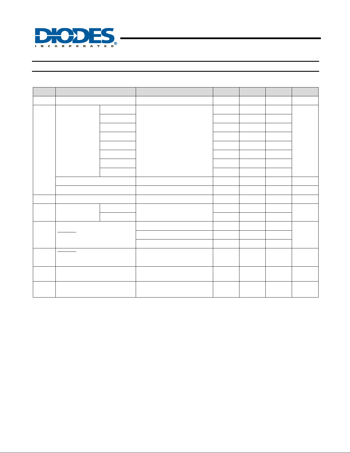
APX803/D
T
Electrical Characteristics (T
TA= -40 to 85°C unless otherwise note. Typical values are at TA=+25 °C.
Symbol Parameter Test Conditions Min Typ. Max Unit
ICC Supply Current V
APX803-23
APX803-26 2.59 2.63 2.66
APX803-29 2.89 2.93 2.96
Reset Threshold
VTH
Reset Threshold hysteresis V
Reset Threshold Tempco 30 ppm/°C
tS VCC to RESET delay V
DELAY
VOL
Reset Active
Timeout Period
TRESE Output Voltage Low
t
APX803D-29 2.89 2.93 2.96
APX803-31 3.04 3.08 3.13
APX803-40 3.94 4.00 4.06
APX803-44 4.31 4.38 4.45
APX803-46 4.56 4.63 4.70
APX803-XX
APX803D-29 1 3.3
= 25°C)
A
T
T
V
V
+ 0.2V 30 40 μA
TH
= 25oC
A
– V
TH-H
CC
A
CC
CC
CC
TH-L
= VTH to (VTH – 100mV) 20 µs
= 0oC to +85oC
= V
-0.2, I
TH
= V
-0.2, I
TH
> 1.0V, I
3-PIN MICROPROCESSOR RESET CIRCUIT
2.21 2.25 2.30
40 mV
140 200 280
= 1.2mA 0.3
SINK
= 3.5mA 0.4
SINK
= 50uA 0.3
SINK
V
ms
V V
IOH
θ
JA
θ
JC
Notes: 2. Test condition for SOT23 and SOT23R: Devices mounted on FR-4 substrate PC board, 2oz copper, with minimum
recommended pad layout.
3. Final datasheet limits to be determined by characterization and correlation.
TRESE Output High leakage
current
Thermal Resistance Junction-to-
Ambient
hermal Resistance
Junction-to-Case
V
> V
CC
+0.2 1 µA
TH
SOT23/SOT23R (Note 2) 201 °C/W
SOT23/SOT23R (Note 2) 56 °C/W
APX803
Document number: DS32132 Rev. 2 - 2
4 of 11
www.diodes.com
September 2010
© Diodes Incorporated
Page 5

V
Typical Performance Characteristics
APX803/D
3-PIN MICROPROCESSOR RESET CIRCUIT
RE SE T Threshold Voltage vs. Temperature
5.0
4.5
4.0
3.5
3.0
2.5
RESET Threshold Voltage(
2.0
-50-250 255075100
APX803-26
Temperature (°C)
Figure 1
RE SE T Timeout Period vs. Temperature
250
APX803
240
230
220
210
200
190
180
170
160
RESET Timeout Period(ms)
150
-50-250 255075100
Temperature (°C)
RE SET Threshold Voltage vs. Temperature
5.0
4.5
4.0
3.5
3.0
2.5
RESET Threshold Voltage(V
2.0
-50 -25 0 25 50 75 100
APX803-44
Temperature (°C)
Figure 2
RE SE T Timeout Period vs. Temperature
3.00
APX803D
2.80
2.60
2.40
2.20
2.00
1.80
1.60
1.40
1.20
RESET Timeout Period(ms)
1.00
-50 -25 0 25 50 75 100
Temperature ( °C)
Figure 3
Supply Current vs. Temperature
30
Vcc=3. 3V
29
28
27
26
25
24
23
22
Vcc Supply Current(uA)
21
20
-50 -25 0 25 50 75 100
Temperature (°C)
40
35
30
25
20
15
10
Supply Current(uA )
5
0
0123456
Figure 5
APX803
Document number: DS32132 Rev. 2 - 2
5 of 11
www.diodes.com
Figure 4
Supply Current vs. Vcc
Vcc(V)
Figure 6
September 2010
© Diodes Incorporated
Page 6

V
V
V
V
3-PIN MICROPROCESSOR RESET CIRCUIT
Typical Performance Characteristics (Continued)
APX803/D
Nch Driver Sink Current vs. Vcc
60
APX803- 26 VDS=0.5V
50
40
30
20
Sink Current I sink(mA )
10
0
0.0 0.5 1.0 1.5 2.0 2.5 3.0
25ºC
-40ºC
85ºC
Vcc(V)
Figure 7 Figure 8
80
70
60
50
40
30
20
10
Nch Driv er Output Current(mA)
0
Nch Driver Output C urrent vs . V
APX803-26
cc= 2.5V
cc= 2.0V
cc= 1.5V
0.0 0.5 1.0 1.5 2.0 2.5 3.0
VDS(V)
DS
Nch Driver S ink Cu rr en t vs. Vcc
60
A PX 803- 44 VDS=0.5V
50
25ºC
40
30
20
10
Sink Current Is i nk (m A )
0
0.0 1.0 2.0 3.0 4.0 5.0
-40ºC
85ºC
Vcc(V)
Nch Driver Output Current vs. V
100
APX803-44
90
80
70
60
50
40
30
20
10
Nch Driver Out p ut Current(mA)
0
0.00.51.01.52.02.53.03.54.0
Vcc= 2.0V
Vcc= 1.5V
VDS(V)
Vcc= 3.0V
Vcc= 2.5V
DS
Vcc= 4.0V
cc= 3.5V
Figure 9 Figure 10
APX803
Document number: DS32132 Rev. 2 - 2
6 of 11
www.diodes.com
September 2010
© Diodes Incorporated
Page 7

Timing Diagram
Vth
Vcc
Vth
T
Delay
/RESET
Vth
T
Delay
RESET
Functional Description
Microprocessors (µPs) and microcontrollers (µC) have a
reset input to ensure that it starts up in a known state.
The APX803/D drive the µP’s reset input to prevent
code-execution errors during power-up, power-down, or
brownout conditions. They assert a reset signal
whenever the V
preset threshold and keep it asserted for a fixed period
of time after V
the APX803D this period is a minimum of 1ms while for
other APX803 variants it is at least 140ms. The
APX803/D have an open-drain output stage.
Ensuring a Valid Reset Output
Down to V
RESET
Once V
keeps
this interval,
occurs (V
RESET
threshold, the internal timer resets to zero, and
goes low. The internal timer starts after V
above the reset threshold, and
the reset timeout period.
CC
is guaranteed to be a logic low for VCC > 1V.
exceeds the reset threshold, an internal timer
CC
RESET
CC
goes low. Any time VCC goes below the reset
supply voltage declines below a
CC
has risen above the reset threshold. For
CC
= 0
low for the reset timeout period; after
RESET
dips below the
goes high. If a brownout condition
RESET
reset threshold),
RESET
remains low for
CC
RESET
returns
APX803/D
3-PIN MICROPROCESSOR RESET CIRCUIT
T
Delay
T
Delay
When VCC falls below 1V, the APX803/D
output no longer sinks current — it becomes an open
circuit. Therefore, high-impedance CMOS logic inputs
connected to
RESET
This presents no problem in most applications since
most µP and other circuitry is inoperative with VCC below
1V.
Interfacing to µP with Bidirectional Reset Pins
Since the RESET output on the APX803/D is open drain,
this device interfaces easily with μP/µC that have
bidirectional reset pins, such as the Motorola 68HC11.
Connecting the μP supervisor’s RESET output directly to
the microcontroller’s (μC’s) RESET pin with a single pullup resistor allows either device to assert reset.
Supervising and monitoring Multiple Supplies
Generally, the pull-up resistor connected to the
APX803/D will connect to the supply voltage that is being
monitored at the IC’s V
may use the APX803/D open-drain output to level-shift
from the monitored supply to reset the µP powered by a
different supply voltage or monitor multiple supplies that
will be fed into 1 µC/µP reset input.
can drift to undetermined voltages.
pin. However, some systems
CC
RESET
APX803
Document number: DS32132 Rev. 2 - 2
7 of 11
www.diodes.com
September 2010
© Diodes Incorporated
Page 8

Ordering Information
APX803/D
3-PIN MICROPROCESSOR RESET CIRCUIT
APX 8 03 - XX XX G - 7
Output type
03 : Active-Low,
Open Drain
Voltage
46 : 4.63
44 : 4.38
40 : 4.00
31 : 3.08
29 : 2.93
26 : 2.63
23 : 2.25
Package
SA : SOT23
SR : SOT23R
Green
G : Green
Packing
7 : Tape & Reel
APX 8 03 D - 29 XX G - 7
Output type
03 : Active-Low,
Open Drain
Device Package Code
APX803-XXSAG-7 SA SOT23 3000/Tape & Reel -7
APX803-XXSRG-7 SR SOT23R 3000/Tape & Reel -7
APX803D-29SAG-7 SA SOT23 3000/Tape & Reel -7
APX803D-29SRG-7 SR SOT23R 3000/Tape & Reel -7
Notes: 4. Pad layout as shown on Diodes Inc. suggested pad layout document AP02001, which can be found on our website at
http://www.diodes.com/datasheets/ap02001.pdf.
Voltage
29 : 2.93
Packaging
(Note 4)
Package
SA : SOT23
SR : SOT23R
Green
G : Green
7” Tape and Reel
Quantity Part Number Suffix
Packing
7 : Tape & Reel
APX803
Document number: DS32132 Rev. 2 - 2
8 of 11
www.diodes.com
September 2010
© Diodes Incorporated
Page 9

Marking Information
(1) SOT23 and SOT23R
APX803/D
3-PIN MICROPROCESSOR RESET CIRCUIT
( Top View )
XX
3
Y W
X
XX : Identification code
: Year 0~9
Y
W
: Week : A~Z : 1~26 week;
a~z : 27~52 week; z represents
52 and 53 week
X
1 2
: A~Z : Green
Device Package Identification Code
APX803-46SA SOT23 V3
APX803-44SA SOT23 V4
APX803-40SA SOT23 V5
APX803-31SA SOT23 V6
APX803-29SA SOT23 V7
APX803-26SA SOT23 V8
APX803-23SA SOT23 V9
APX803-46SR SOT23R S3
APX803-44SR SOT23R S4
APX803-40SR SOT23R S5
APX803-31SR SOT23R S6
APX803-29SR SOT23R S7
APX803-26SR SOT23R S8
APX803-23SR SOT23R S9
APX803D-29SA SOT23 VN
APX803D-29SR SOT23R SN
APX803
Document number: DS32132 Rev. 2 - 2
9 of 11
www.diodes.com
September 2010
© Diodes Incorporated
Page 10

3-PIN MICROPROCESSOR RESET CIRCUIT
Package Outline Dimensions (All Dimensions in mm)
(1) Package Type: SOT23 and SOT23R
APX803/D
Notes: 5. Package outline dimensions as shown on Diodes Inc. package outline dimensions document AP02002, which can be found on
our website at http://www.diodes.com/datasheets/ap02002.pdf
APX803
Document number: DS32132 Rev. 2 - 2
10 of 11
www.diodes.com
September 2010
© Diodes Incorporated
Page 11

APX803/D
3-PIN MICROPROCESSOR RESET CIRCUIT
IMPORTANT NOTICE
DIODES INCORPORATED MAKES NO WARRANTY OF ANY KIND, EXPRESS OR IMPLIED, WITH REGARDS TO THIS
DOCUMENT, INCLUDING, BUT NOT LIMITED TO, THE IMPLIED WARRANTIES OF MERCHANTABILITY AND FITNESS FOR A
PARTICULAR PURPOSE (AND THEIR EQUIVALENTS UNDER THE LAWS OF ANY JURISDICTION).
Diodes Incorporated and its subsidiaries reserve the right to make modifications, enhancements, improvements, corrections or other
changes without further notice to this document and any product described herein. Diodes Incorporated does not assume any liability
arising out of the application or use of this document or any product described herein; neither does Diodes In corporated convey any
license under its patent or trademark rights, nor the rights of others. Any Customer or user of this documen t or products described
herein in such applications shall assume all risks of such use and will agree to hold Diodes Incorporated and all the companies
whose products are represented on Diodes Incorporated website, harmless against all damages.
Diodes Incorporated does not warrant or accept any liability whatsoever in respect of any products purchased through unauthorized
sales channel.
Should Customers purchase or use Diodes Incorporated products for any unintended or unauthorized application, Customers shall
indemnify and hold Diodes Incorporated and its representatives harmless against all claims, damages, expenses, and attorney fees
arising out of, directly or indirectly, any claim of personal injury or death associated with such unintended or unauthorized application.
Products described herein may be covered by one or more United States, international or foreign p atents pending. Product names
and markings noted herein may also be covered by one or more United States, international or foreign trademarks.
LIFE SUPPORT
Diodes Incorporated products are specifically not authorized for use as critical components in life support devices or systems without
the express written approval of the Chief Executive Officer of Diodes Incorporated. As used herein:
A. Life support devices or systems are devices or systems which:
1. are intended to implant into the body, or
2. support or sustain life and whose failure to perform when properly used in accordance with instructions for use provided
in the labeling can be reasonably expected to result in significant injury to the user.
B. A critical component is any component in a life support device or system whose failure to perform can b e reasonably expected
to cause the failure of the life support device or to affect its safety or effectiveness.
Customers represent that they have all necessary expertise in the safety and regulatory ramifications of their life support dev ices or
systems, and acknowledge and agree that they are solely responsible for all legal, regulatory and safety-related requirements
concerning their products and any use of Diodes Incorporated products in such safety-critical, life support devices or systems,
notwithstanding any devices- or systems-related information or support that may be provided by Diodes Incorporated. Further,
Customers must fully indemnify Diodes Incorporated and its representatives against any damages arising out of the use of Diodes
Incorporated products in such safety-critical, life support devices or systems.
Copyright © 2010, Diodes Incorporated
www.diodes.com
APX803
Document number: DS32132 Rev. 2 - 2
11 of 11
www.diodes.com
September 2010
© Diodes Incorporated
 Loading...