

Page 1
APX321/APX358/APX324
LOW VOLTAGE, RAIL-TO-RAIL INPUT AND OUTPUT
SINGLE/DUAL/QUAD OPERATIONAL AMPLIFIERS
Features
(For V+=5V and V-=0V typical unless otherwise noted)
• Guaranteed 2.7V and 5V performance
• Crossover distortion eliminated
• Operating temperature range (-40°C to +85°C)
• Gain-bandwidth 1 MHz
• Low supply current
• APX321 110 µA Typ
• APX358 190 µA Typ
• APX324 340 µA Typ
• Rail-to-rail output swing @ 10 kΩ
• Input Common Mode Voltage Range (0 to V
• Manufactured in standard CMOS process
• SOT353, SOT25, MSOP-8L, SOP-8L and TSSOP-14L:
Available in “Green” Molding Compound (No Br, Sb)
• Lead-free Finish / RoHS Compliant (Note 4)
• V
• V
+
-10 mV
-
+10 mV
+
Applications
• Active filters
• General purpose low voltage applications
• General purpose portab l e devices
Ordering Information
General Description
The APX321/APX358/APX324 are low voltage (2.5V to 5.5V)
single, dual and quad operational amplifiers. The
APX321/APX358/APX324 are designed to effectively reduce cost
and space at low voltage levels. These devices have the
capability of rail-to-rail output swing and input common-mode
voltage range. They can also achieve an efficient speed-to-power
ratio, utilizing 1 MHz bandwidth and 1 V/µs slew rate at a low
supply current. Reducing noise pickup and increasing signal
integrity can be achieved by placing the device close to the signal
source.
packages that reduce space on pc boards and portable
electronic devices.
-0.2V)
APX3 XX XX G - 13
package. The APX358 is available in the MSOP-8L and SOP-8L
packages.
The APX321 is available in 5-Pin SOT353/SOT25
The APX324 is available in the TSSOP-14L
Packing
7/13 : Tape & Reel
Device
Part Number
21 : Single (Note 1)
24 : Quad (Note 2)
58 : Dual (Note 3)
Package
Code
Package
W : SOT25
SE : SOT353
TS : TSSOP-14L
S : SOP8L
M8 : MSOP-8L
Packaging
(Note 5)
Green
G : Green
7”/13” Tape and Reel
Quantity Part Number Suffix
APX321WG-7 W SOT25 3000/Tape & Reel -7
APX321SEG-7 SE SOT353 3000/Tape & Reel -7
APX324TSG-13 TS TSSOP-14L 2500/Tape & Reel -13
APX358SG-13 S SOP-8L 2500/Tape & Reel -13
APX358M8G-13 M8 MSOP-8L 2500/Tape & Reel -13
Notes: 1. APX321 is only available for SOT25 and SOT353.
2. APX324 is only available for TSSOP-14L.
3. APX358 is only available for SOP-8L and MSOP-8L.
4. EU Directive 2002/95/EC (RoHS). All applicable RoHS exemptions applied. Please visit our website at
http://www.diodes.com/products/lead_free.html
5. Pad layout as shown on Diodes Inc. suggested pad layout document AP02001, which can be found on our website at
http://www.diodes.com/datasheets/ap02001.pdf.
APX321/APX358/APX324 Rev. 13 1 of 18 FEBRUARY 2009
www.diodes.com © Diodes Incorporated
Page 2
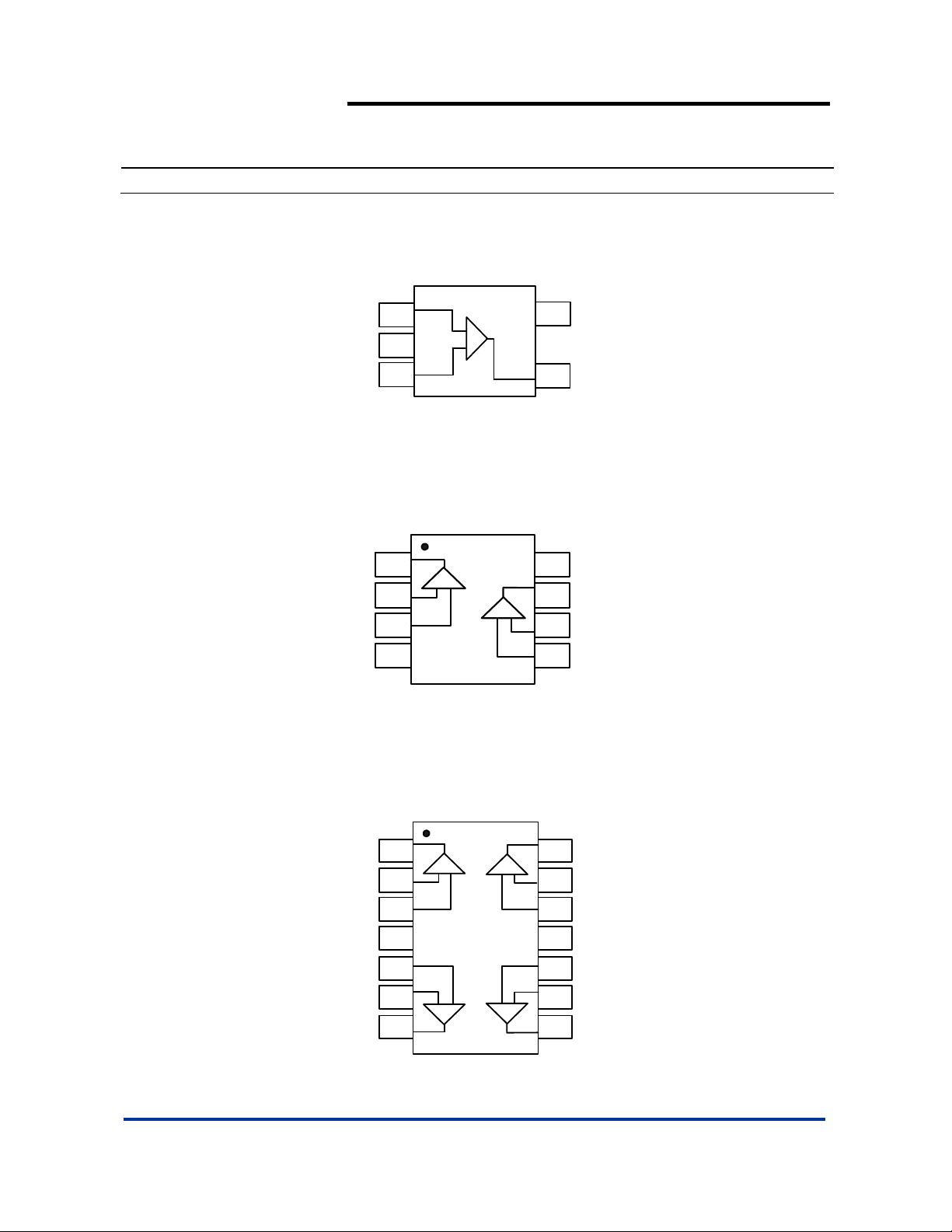
Pin Assignments
(1) SOT25 / SOT353
APX321/APX358/APX324
LOW VOLTAGE, RAIL-TO-RAIL INPUT AND OUTPUT
SINGLE/DUAL/QUAD OPERATIONAL AMPLIFIERS
( Top View )
(2) SOP-8L / MSOP-8L
(3) TSSOP-14L
IN
OUT
IN
IN
V
1
V
IN
+
-
2
3
-
+
-
SOT25 / SOT353
( Top View )
1
A+
A
A-
2
3
-
- +
A
SOP-8L / MSOP-8L
(Top View)
+ -
+
5
V
OUT
4
8
7
B
6
54
+
V
OUT
B-
IN
B+
IN
B
OUT
IN
IN
OUT
IN
IN
1
A
2
-
A
3
A
+
+
4
V
B
+
5
-
B
6
B
7
A
+
-
-
+
B
+
+
D
-
-
C
TSSOP-14L
APX321/APX358/APX324 Rev. 13 2 of 18 FEBRUARY 2009
www.diodes.com © Diodes Incorporated
14
13
12
11
10
9
8
OUT
IN
D
IN
D
-
V
IN
C
IN
C
OUT
D
-
+
+
-
C
Page 3
APX321/APX358/APX324
LOW VOLTAGE, RAIL-TO-RAIL INPUT AND OUTPUT
SINGLE/DUAL/QUAD OPERATIONAL AMPLIFIERS
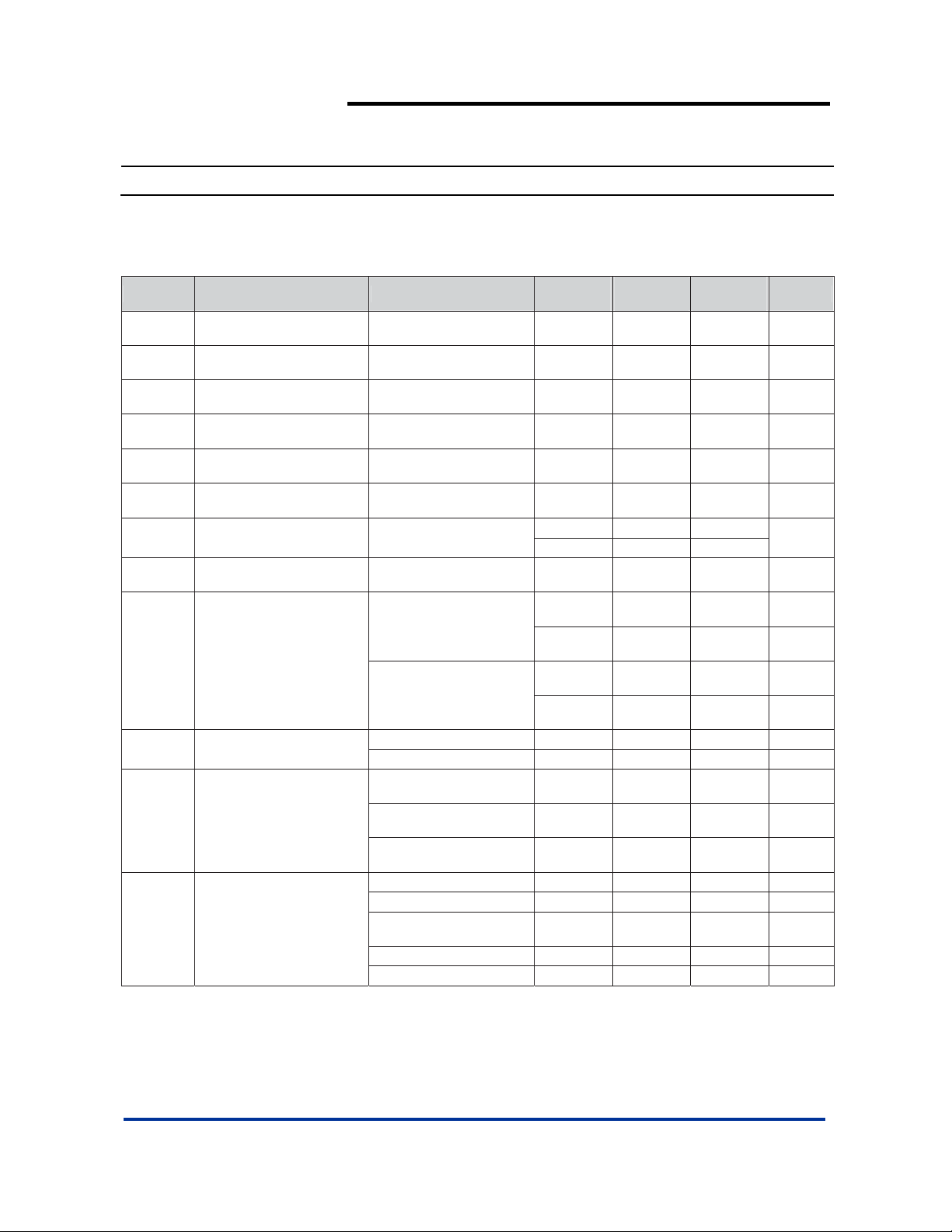
Absolute Maximum Ratings (Note 6)
Symbol Description Rating Unit
ESD HBM
ESD MM Machine Model ESD Protection
Differential Input Voltage ±Supply Voltage V
V+ -V
Output Short Circuit to V+ (Note 7)
Output Short Circuit to V- (Note 8)
TST Storage Temperature -65 to 150 °C
TJ Maximum Junction Temperature 150 °C
Human Body Model ESD
Protection
-
Supply Voltage 5.5 V
APX321
APX324
APX321 350
APX324 250
Operating Ratings (Note 6)
Symbol Description Rating Unit
V+ -V- Supply Voltage 2.5 to 5.5 V
TA Operatin g Am bi ent Temperatur e Range
Notes: 6. Absolute Maximum Ratings indicate limits beyond which damage to the device may occur. Operating Ratings indicate conditions for which the
device is intended to be functional, but specific performance is not guaranteed. For guaranteed specifications and the test conditions, see the
Electrical Characteristics.
4000
4000
4500
-40 to +85
V APX358
V APX358 350
°C
APX321/APX358/APX324 Rev. 13 3 of 18 FEBRUARY 2009
www.diodes.com © Diodes Incorporated
Page 4
APX321/APX358/APX324
LOW VOLTAGE, RAIL-TO-RAIL INPUT AND OUTPUT
SINGLE/DUAL/QUAD OPERATIONAL AMPLIFIERS
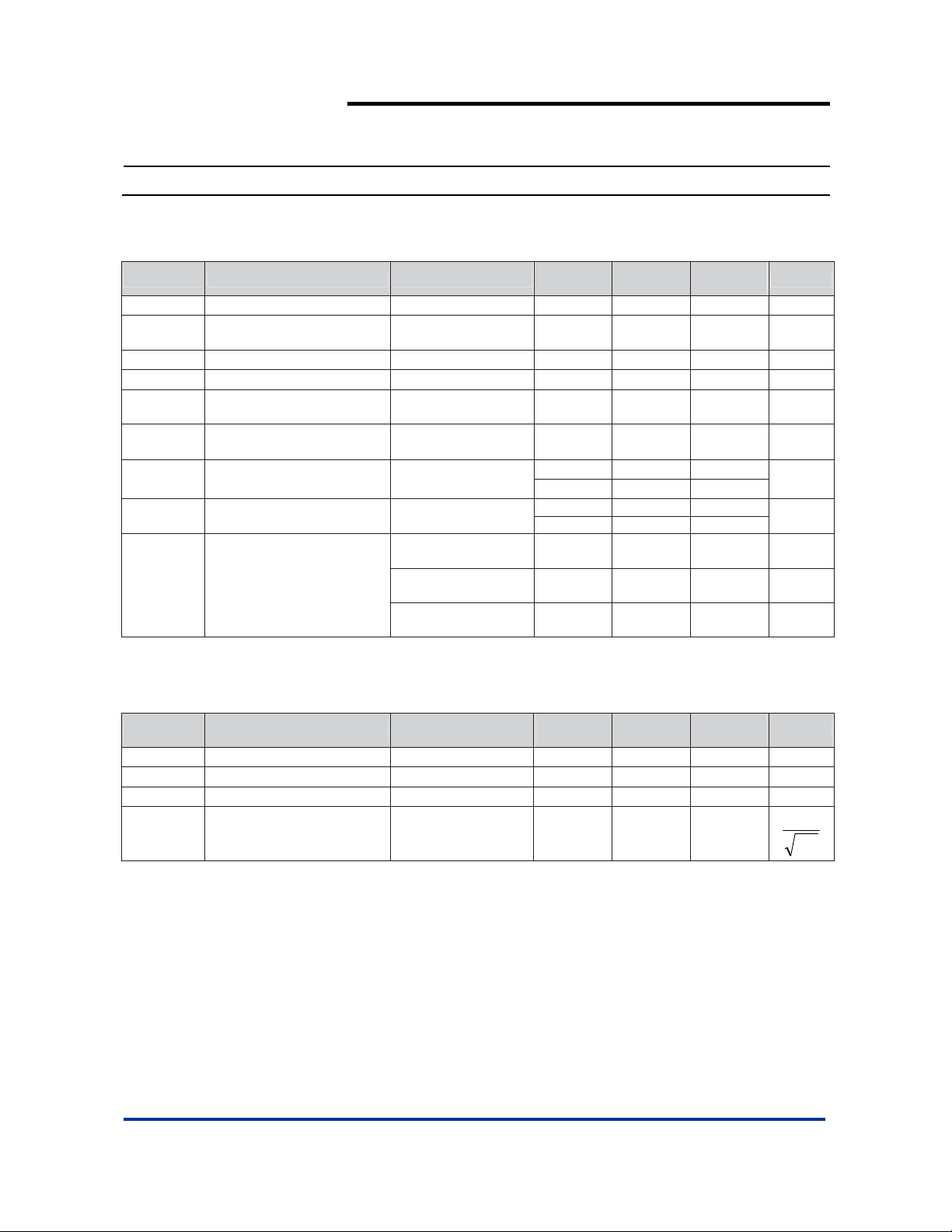
Electrical Characteristics
2.7V DC Electrical Characteristics
Unless otherwise specified, all limits guaranteed for TA = 25°C, V+ = 2.7V, V- = 0V, VCM = 1.0V, VO = V+/2 and RL > 1 MΩ.
Symbol Parameter Test Conditions
Min
(Note 10)
VOS Input Offset Voltage 1.7 7 mV
TCVOS
Input Offset Voltage
Average Drift
5 µV/°C
IB Input Bias Current 10 nA
IOS Input Offset Current 5 50 nA
CMRR
PSRR
V
CMR
VO Output Swing RL = 10 kΩ to 1.35V
IS Supply Current
Common Mode Rejection
Ratio
Power Supply Rejection
Ratio
Input Common-Mode
Voltage Range
0V ≤ V
2.7V ≤ V
V
O
= 1V
≤ 2.4V
CM
+
≤ 5V
For CMRR ≥ 50dB
APX321
Single amplifier
APX358
Both amplifiers
APX324
All four amplifiers
50 63 dB
50 60 dB
0 -0.2
2.5
+
- 100 V+ - 20
V
20 100
110 140 µA
190 340 µA
340 680 µA
2.7V AC Electrical Characteristics
Unless otherwise specified, all limits guaranteed for TA = 25°C, V+ = 2.7V, V- = 0V, VCM = 1.0V, VO = V+/2 and RL > 1 MΩ.
Symbol Parameter Test Conditions
Min
(Note 10)
GBWP Gain-Bandwidth Product CL = 200 pF 1 MHz
Φm
Phase Margi n 60 Deg
Gm Gain Margin 10 dB
en
Input-Referred Voltage
Noise
f > 50 KHz 23
Typ.
(Note 9)
Typ.
(Note 9)
Max
(Note 10)
Max
(Note 10)
Unit
V
mV
Unit
nV
H
Z
APX321/APX358/APX324 Rev. 13 4 of 18 FEBRUARY 2009
www.diodes.com © Diodes Incorporated
Page 5
APX321/APX358/APX324
LOW VOLTAGE, RAIL-TO-RAIL INPUT AND OUTPUT
SINGLE/DUAL/QUAD OPERATIONAL AMPLIFIERS
Electrical Characteristics (Continued)
5V DC Electrical Characteristics
Unless otherwise specified, all limits guaranteed for TA = 25°C, V+ = 5V, V- = 0V, VCM = 2.0V, VO = V+/2 and
> 1 MΩ. Boldface limits apply at the temperature extremes.
R
L
Symbol Parameter Test Conditions
VOS Input Offset Voltage
TCVOS
Input Offset Voltage
Average Drift
5 µV/°C
IB Input Bias Current
IOS Input Offset Current
CMRR
PSRR
V
Common Mode Rejection
Ratio
Power Supply Rejection
Ratio
Input Common-Mode
CMR
Voltage Range
0V ≤ V
2.7V ≤ V
V
O
≤ 4.7V
CM
+
≤ 5V
= 1V, VCM = 1V
For CMRR ≥ 50dB
AV Large Signal Voltage Gain RL = 2 kΩ (Note 11)
R
= 2 kΩ to 2.5V
L
VO Output Swing
RL = 10 kΩ to 2.5V
Output Short Circuit
IO
Current
Sourcing, V
Sinking, VO = 5V 10 90 mA
= 0V 5 60 mA
O
APX321
Single amplifier
IS Supply Current
APX358
Both amplifiers
APX324
All four amplifiers
SOT353 (Note 12) 330 °C/W
SOT25 (Note 12) 250 °C/W
θ
Thermal Resistance
JA
Junction-to-Ambient
TSSOP-14L
(Note 12)
MSOP-8L (Note 12) 203 °C/W
SOP-8L (Note 12) 150 °C/W
Min
(Note 10)
50 65 dB
50 60 dB
0 -0.2
4.8
15
10
+
- 300
V
+
- 400
V
+
V
- 100
+
V
- 200
110 140 µA
100 °C/W
Typ.
(Note 9)
1.7
15
5
100
+
V
- 50
50
+
- 10
V
10
190
340
Max
(Note 10)
7
9
250
500
50
150
Unit
mV
nA
nA
V
V/mV
mV
300
400
mV
mV
180
280
340
600
680
1100
mV
µA
µA
APX321/APX358/APX324 Rev. 13 5 of 18 FEBRUARY 2009
www.diodes.com © Diodes Incorporated
Page 6
APX321/APX358/APX324
LOW VOLTAGE, RAIL-TO-RAIL INPUT AND OUTPUT
SINGLE/DUAL/QUAD OPERATIONAL AMPLIFIERS
Electrical Characteristics (Continued)
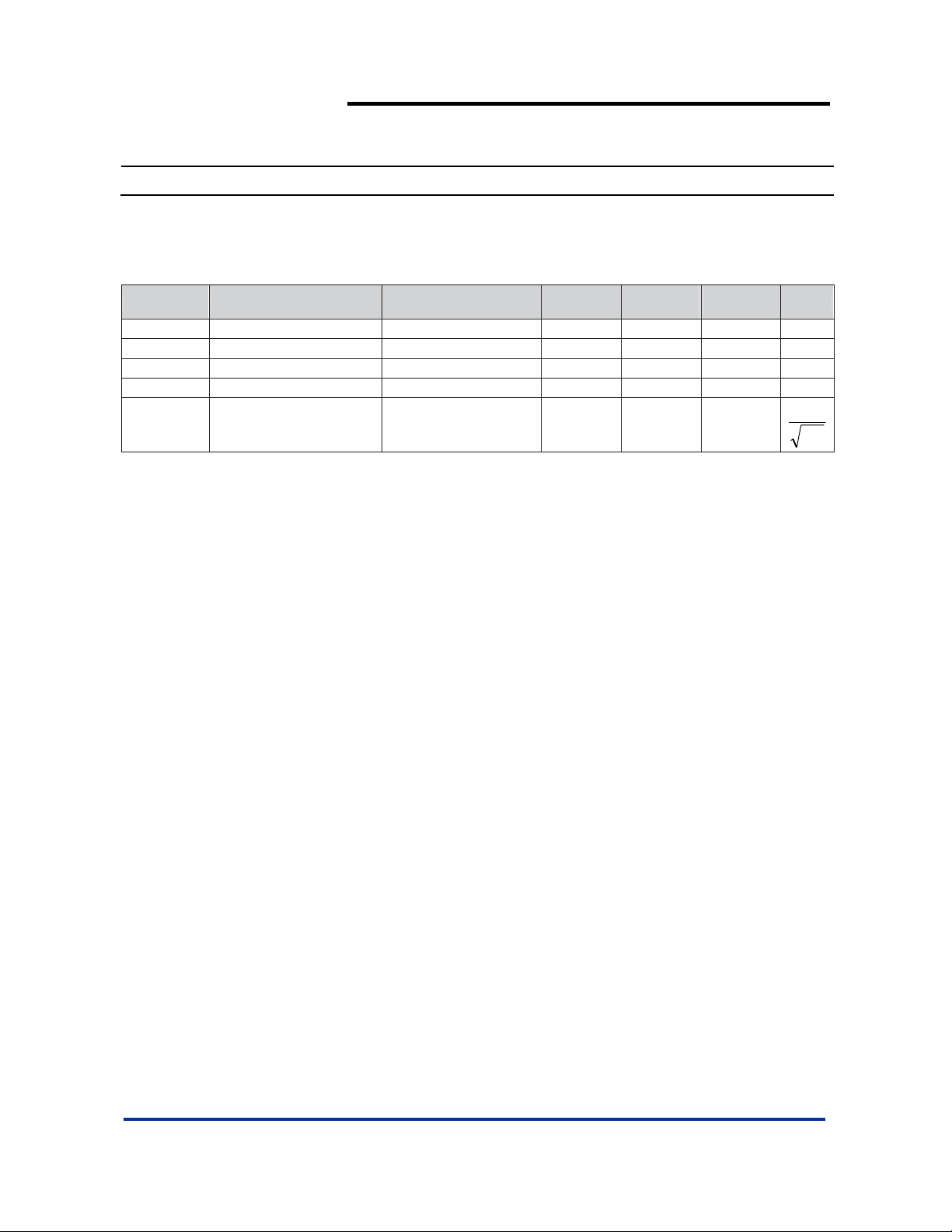
5V AC Electrical Characteristics
Unless otherwise specified, all limits guaranteed for TA = 25°C, V+ = 5V, V- = 0V, VCM = 2.0V, VO = V+/2 and RL > 1 MΩ. Boldface limits
apply at the temperature extremes.
Symbol Parameter Test Conditions
Min
(Note 10)
SR Slew Rate (Note 13) 1 V/µs
GBWP Gain-Bandwidth Product CL = 200 pF 1 MHz
Φ
Phase Margin 60 Deg
m
Gm Gain Margin 10 dB
en
Notes: 7. Shorting output to V+ will adversely affect r e liability.
8. Shorting output to V- will adversely affect reliability.
9. Typical values represent the most likely parametric norm as determined at the time of characterization. Actual typical values may vary over time
and will also depend on the application and configuration. The typical values are not tested and are not guaranteed on shipped production
material.
10. All limits are guaranteed by testing or statistical analysis.
11. R
Input-Refer r e d V o ltage
Noise
is connected to V-. The output voltage is 0.5V ≤ VO ≤ 4.5V.
L
12. All numbers are typical, and apply for packages soldered directly onto a PC board in still air.
13. Connected as voltage follower with 3V step input. Number specified is the slower of the positive and negative slew rates.
f > 50 KHz 23
APX321/APX358/APX324 Rev. 13 6 of 18 FEBRUARY 2009
www.diodes.com © Diodes Incorporated
Typ.
(Note 9)
Max
(Note 10)
Unit
nV
H
Z
Page 7

C
m
V
APX321/APX358/APX324
LOW VOLTAGE, RAIL-TO-RAIL INPUT AND OUTPUT
SINGLE/DUAL/QUAD OPERATIONAL AMPLIFIERS
Typical Performance Characteristics
Unless otherwise specified, Vs=+5V, single supply, TA=25oC
Supply Current vs. Supply Voltage Output Voltage Swing vs. Supply Voltage
0.24
0.22
0.20
0.18
A)
0.16
0.14
0.12
urrent (
0.10
0.8
0.6
Supply
0.4
0.2
0.0
PSRR vs. Frequency CMRR vs. Frequency
80
70
60
50
40
30
PSRR (dB)
20
10
0
100 1k 10k 100k 1M
CMRR vs. Input Common Mode Voltage ∆
90
85
80
75
70
65
CMRR (dB)
60
55
50
012345
Input Common Mode Voltage (V)
20354
1
Supply Voltage (V)
Frequency (Hz)
Vs = 5V
f = 10KHz
R
L = 5Kohm
Vs = 5V
L = 10Kohm
R
Output Voltage from Power Supply (mV)
100
90
80
70
60
CMRR (dB)
50
40
30
1.2
1.0
0.8
0.6
0.4
δVos (mV)
0.2
0.0
-0.2
6.0
5.5
5.0
4.5
4.0
3.5
3.0
2.5 3.0 3.5 4.0 4.5 5.0
Negative Swing
RL=10Kohm
Positive Swing
Supply Voltage (V)
Vs = 5V
IN = Vs / 2
V
L = 5Kohm
R
100 1k 10k 100k 1M
Frequency (Hz)
os vs. CMR
-3 -2 -1 0 1 2 3
Vcm (V)
APX321/APX358/APX324 Rev. 13 7 of 18 FEBRUARY 2009
www.diodes.com © Diodes Incorporated
Page 8

APX321/APX358/APX324
LOW VOLTAGE, RAIL-TO-RAIL INPUT AND OUTPUT
SINGLE/DUAL/QUAD OPERATIONAL AMPLIFIERS
Typical Performance Characteristics (Continued)
Sourcing Current vs. Output Voltage (2.7V) Sourcing Current vs. Output Voltage (5V)
100
10
1
0.1
sourcing current-mA
0.01
1E-3
1E-3 0.01 0.1 1 10
Output voltage referenced to Vcc-V
VCC=2.7V
Sinking Current vs. Output Voltage (2.7V) Sinking Current vs. Output Voltage (5V)
100
100
10
1
0.1
sourcing current-mA
0.01
1E-3
1E-3 0.01 0.1 1 10
Output voltage referenced to V c c-V
100
Vcc=5V
10
1
0.1
sinking current-mA
0.01
1E-3
1E-3 0.01 0.1 1 10
Output voltage referenced to GND-V
Vcc=2.7V
Input Voltage vs. Output Voltage
2.0
RL=10kohm
RL=2k ohm
1.5
1.0
output voltage(V)
0.5
RL=600ohm
Vs=+/- 2V
10
1
Vcc=5V
0.1
sinking current-mA
0.01
1E-3
1E-3 0.01 0.1 1 10
Output voltage referenced to GND-V
0.0
0 50 100 150 200 250 300
Input voltage(uV)
APX321/APX358/APX324 Rev. 13 8 of 18 FEBRUARY 2009
www.diodes.com © Diodes Incorporated
Page 9

APX321/APX358/APX324
LOW VOLTAGE, RAIL-TO-RAIL INPUT AND OUTPUT
SINGLE/DUAL/QUAD OPERATIONAL AMPLIFIERS
Typical Performance Characteristics (Continued)
Frequency Response vs. Resistive Load (2.7V) Frequency Response vs. Resistive Load (5V)
Frequency Response vs. Capacitive Load (2.7V) Frequency Response vs. Capacitive Load (5V)
Non-Inverting Large Signal Pulse Response Non-Inverting Large Signal Pulse Response
APX321/APX358/APX324 Rev. 13 9 of 18 FEBRUARY 2009
www.diodes.com © Diodes Incorporated
Page 10

APX321/APX358/APX324
LOW VOLTAGE, RAIL-TO-RAIL INPUT AND OUTPUT
SINGLE/DUAL/QUAD OPERATIONAL AMPLIFIERS
Typical Performance Characteristics (Continued)
Non-Inverting Large Signal Pulse Response Non-Inverting Small Signal Pulse Response
Non-Inverting Small Signal Pulse Response Non-Inverting Small Signal Pulse Response
Inverting Large Signal Pulse Response Inverting Large Signal Pulse Response
APX321/APX358/APX324 Rev. 13 10 of 18 FEBRUARY 2009
www.diodes.com © Diodes Incorporated
Page 11

APX321/APX358/APX324
LOW VOLTAGE, RAIL-TO-RAIL INPUT AND OUTPUT
SINGLE/DUAL/QUAD OPERATIONAL AMPLIFIERS
Typical Performance Characteristics (Continued)
Inverting Large Signal Pulse Response Inverting Small Signal Pulse Response
Inverting Small Signal Pulse Response Inverting Small Signal Pulse Response
Stability vs. Capacitive Load Stability vs. Capacitive Load
APX321/APX358/APX324 Rev. 13 11 of 18 FEBRUARY 2009
www.diodes.com © Diodes Incorporated
Page 12

APX321/APX358/APX324
LOW VOLTAGE, RAIL-TO-RAIL INPUT AND OUTPUT
SINGLE/DUAL/QUAD OPERATIONAL AMPLIFIERS
Typical Performance Characteristics (Continued)
Stability vs. Cap aci tive Load Stability vs. Capacitive Load
Slew Rate vs. Supply Voltage Input Voltage Noise
100
90
80
70
60
nV
50
H
Z
40
Slew R a te (V /us )
Supply Voltage (V)
30
20
10
0
1000 10000 100000 1000000
Frequency (Hz)
APX321/APX358/APX324 Rev. 13 12 of 18 FEBRUARY 2009
www.diodes.com © Diodes Incorporated
Page 13

APX321/APX358/APX324
LOW VOLTAGE, RAIL-TO-RAIL INPUT AND OUTPUT
SINGLE/DUAL/QUAD OPERATIONAL AMPLIFIERS
Typical Performance Characteristics (Continued)
Input Voltage Noise (2.7V)
100
90
80
70
60
nV
50
H
Z
40
30
20
10
0
1000 10000 100000 1000000
Frequency (Hz)
APX321/APX358/APX324 Rev. 13 13 of 18 FEBRUARY 2009
www.diodes.com © Diodes Incorporated
Page 14

Marking Information
(1) SOT25 / SOT353
APX321/APX358/APX324
LOW VOLTAGE, RAIL-TO-RAIL INPUT AND OUTPUT
SINGLE/DUAL/QUAD OPERATIONAL AMPLIFIERS
( Top View )
(2) TSSOP-14L
Part Number
(3) SOP-8L
Logo
W X
7
4
XX : Identification code
: Year 0~9
Y
: Week : A~Z : 1~26 week;
W
a~z : 27~52 week; z represents
52 and 53 week
: A~Z : Green
X
5
XX
Y
1 2 3
Device Package type Identification Code
APX321W SOT25 V2
APX321SE SOT353 V3
( Top View )
14
8
G : Green
: Year : 08, 09,10~
APX324
YY WW X X
YY
WW : Week : 01~52; 52
represents 52 and 53 week
: Internal Code
X
1
7
( Top View )
X
5
G : Green
YY
: Year : 08, 09,10~
WW : Week : 01~52; 52
represents 52 and 53 week
: Internal Code
X
41
8
Logo
Part Number
APX321/APX358/APX324 Rev. 13 14 of 18 FEBRUARY 2009
APX358
YY
WW X
www.diodes.com © Diodes Incorporated
Page 15

LOW VOLTAGE, RAIL-TO-RAIL INPUT AND OUTPUT
SINGLE/DUAL/QUAD OPERATIONAL AMPLIFIERS
Marking Information (Continued)
(4) MSOP-8L
( Top View )
8765
Logo
Part Number
APX358
234
1
Y
W X
APX321/APX358/APX324
A~Z : Green
: Year : 0~9
Y
W
: Week : A~Z : 1~26 week;
a~z : 27~52 week; z represents
52 and 53 week
Package Information (All Dimensions in mm)
(1) Package Type: SOT25
APX321/APX358/APX324 Rev. 13 15 of 18 FEBRUARY 2009
www.diodes.com © Diodes Incorporated
Page 16

LOW VOLTAGE, RAIL-TO-RAIL INPUT AND OUTPUT
SINGLE/DUAL/QUAD OPERATIONAL AMPLIFIERS
Package Information (Continued)
(2) Package Type: SOT353
0.10/0.30
C
2.0/2.2
1.15/1.35
1.8/2.2
L
0.65Bsc.
APX321/APX358/APX324
Gauge Plane
0.25/0.40
DETAIL"A"
C
0.1/0.22
L
0.9/1.0
1.10Max.
0/0.1
(3) Package Type: TSSOP-14L
"A"
APX321/APX358/APX324 Rev. 13 16 of 18 FEBRUARY 2009
www.diodes.com © Diodes Incorporated
Page 17

LOW VOLTAGE, RAIL-TO-RAIL INPUT AND OUTPUT
SINGLE/DUAL/QUAD OPERATIONAL AMPLIFIERS
Package Information (Continued)
(4) Package Type: SOP-8L
3.85/3.95
5.90/6.10
0.10/0.20
Detail "A"
0.62/0.82
APX321/APX358/APX324
0.254
Gauge Plane
Seating Plane
7°~9°
1.27typ
8x-0.60
6x-1.27
8x-1.55
Land Pattern Recommendation
0.3/0.5
4.85/4.95
(Unit: mm)
(5) Package Type: MSOP-8L
5.4
2.9/3.1
1.30/1.50
4.7/5.1
1.75max.
0.15/0.25
0.35max.
45°
8x-0.45
6x-0.65
7°~9°
4.4
Detail "A"
0°/8°
0.65Bsc.
1
0.22/0.38
0.05
2.9/3.1
8x-1.4
Land Pattern Recommendation
0.75/0.95
0.15Typ.
0/0.15
0.05/0.15
0.4/0.8
DETAIL "A"
(Unit:mm)
0.95Ref.
"A"
0.25
Gauge plane
°
8
/
°
0
APX321/APX358/APX324 Rev. 13 17 of 18 FEBRUARY 2009
www.diodes.com © Diodes Incorporated
Page 18

APX321/APX358/APX324
LOW VOLTAGE, RAIL-TO-RAIL INPUT AND OUTPUT
SINGLE/DUAL/QUAD OPERATIONAL AMPLIFIERS
IMPORTANT NOTICE
Diodes Incorporated and its subsidiaries reserve the right to make modifications, enhancements, improvements, corrections or other changes without further
notice to any product herein. Diodes Incorporated does not assume any liability arising out of the application or use of any product described herein; neither
does it convey any license under its patent rights, nor the rights of others. The user of products in such applications shall assume all risks of such use and will
agree to hold Diodes Incorporated and all the companies whose products are represented on our website, harmless against all damages.
LIFE SUPPORT
Diodes Incorporated products are not authorized for use as critical components in life support devices or systems without the expressed written approval of the
President of Diodes Incorporated.
APX321/APX358/APX324 Rev. 13 18 of 18 FEBRUARY 2009
www.diodes.com © Diodes Incorporated
 Loading...