

Page 1
A
Description
The AP7363 is a 1.5A adjustable output voltage linear regulator with
ultra-low dropout. The device includes pass element, error amplifier,
band-gap, current limit and thermal shutdown circuitry.
The characteristics of low dropout voltage and fast transient response
to step changes in load make it suitable for low voltage
microprocessor applications. The typical quiescent current is
approximately 0.5mA and changes little with load current. The built-in
current-limit and thermal-shutdown functions prevent IC from damage
in fault conditions.
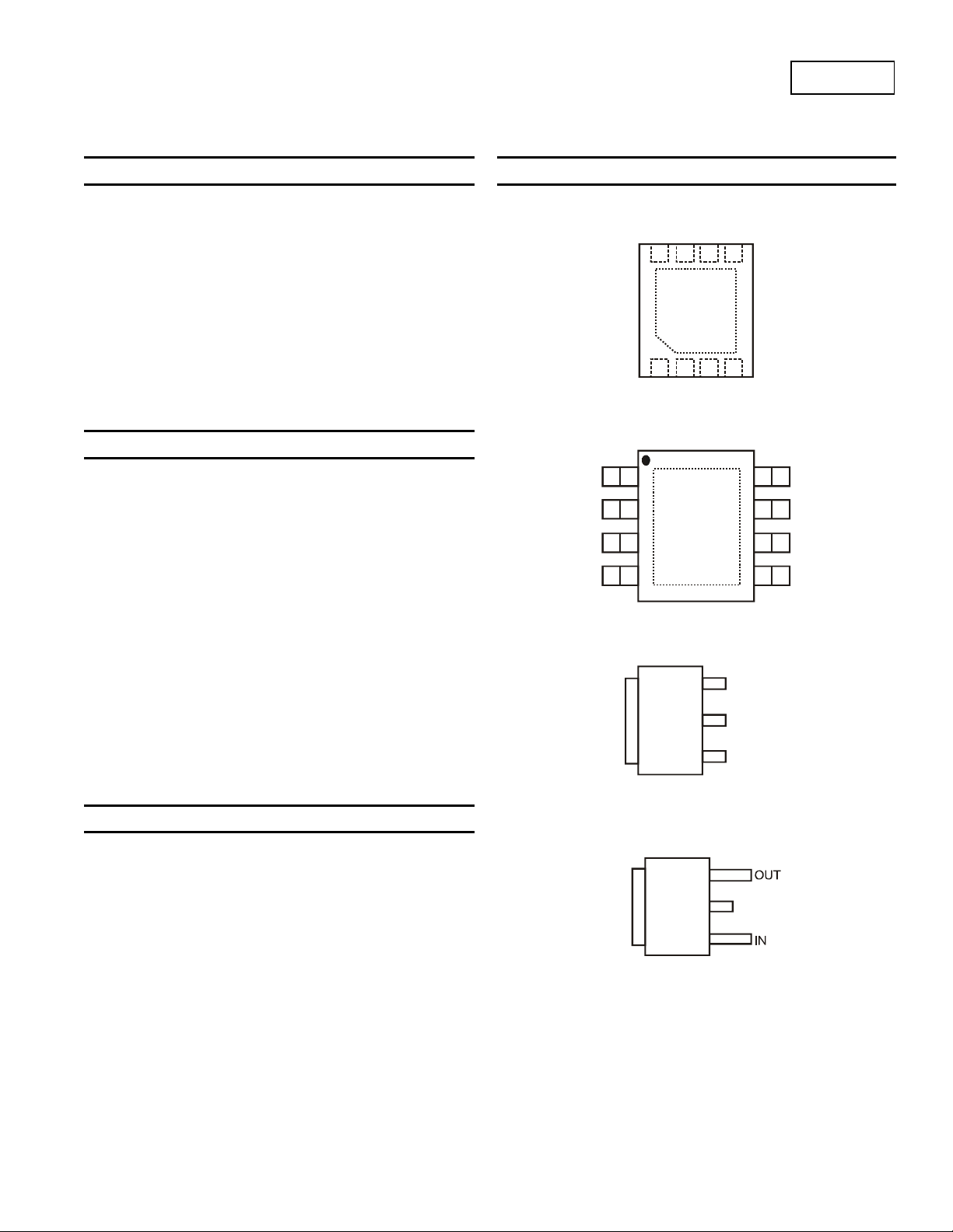
This device is available in U-DFN2030-8, SO-8EP, SOT223 and
TO252 packages.
Features
• 1.5A ultra-low dropout linear regulator
• Ultra-low dropout: 190mV at 1.5A
• Stable with 10µF input/output capacitor, any types
• Wide input voltage range: 2.2V to 5.5V
• Adjustable output voltage: 0.6V to 5.0V
• Fixed output options: 1V, 1.2V, 1.5V, 1.8V, 2.5V, 3.3V
• Low ground pin current
• 25nA quiescent current in shutdown mode
• V
• V
• Excellent Load/Line Transient Response
• Current limit and thermal shutdown protection
• Ambient temperature range: -40°C to +85°C
• U-DFN2030-8, SO-8EP, SOT223 and TO252: Available in
• Totally Lead-Free & Fully RoHS Compliant (Notes 1 & 2)
• Halogen and Antimony Free. “Green” Device (Note 3)
accuracy of ±1.5% @ +25°C
ADJ
accuracy of ±3% over line, load and temperature
ADJ
“Green” Molding Compound (No Br, Sb)
Applications
• ASIC power supplies in printers, graphics cards, DVD players,
STBs, routers, etc
• FPGA and DSP core or I/O power supplies
• SMPS regulator
• Conversion from 3.3V or 5V rail
P7363
1.5A LOW QUIESCENT CURRENT, FAST TRANSIENT
ULTRA-LOW DROPOUT LINEAR REGULATOR
Pin Assignments
(Top View)
GND
1
2
IN
3
IN
IN
4
ADJ/
NC
U-DFN2030-8
(Top View)
SO-8EP
(Top View)
SOT223
(Fixed Output)
(Top View)
OUTOUTOUT
6785
3214
IN INGND
IN
OUT
3
GND (TAB)
2
IN
1
3
2
1
GND
8
ADJ/NC
OUT
7
OUT
6
OUT
5
TO252
Notes: 1. No purposely added lead. Fully EU Directive 2002/95/EC (RoHS) & 2011/65/EU (RoHS 2) compliant.
2. See http://www.diodes.com for more information about Diodes Incorporated’s definitions of Halogen- and Antimony-free, "Green" and Lead-free.
3. Halogen- and Antimony-free "Green” products are defined as those which contain <900ppm bromine, <900ppm chlorine (<1500ppm total Br + Cl)
and <1000ppm antimony compounds.
AP7363
Document number: DS35059 Rev. 8 - 2
1 of 14
www.diodes.com
December 2012
© Diodes Incorporated
Page 2
A
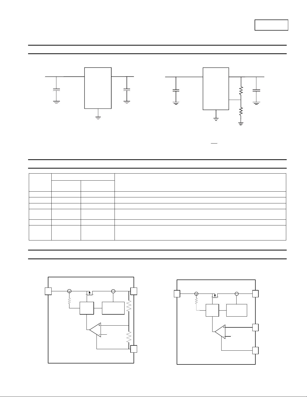
Typical Applications Circuit
V
IN
P7363
V
OUTIN
OUT
V
IN
OUTIN
V
OUT
AP7363
10µF
GND
Fixed Output
10µF
Pin Descriptions
Pin
Name
SOT223
TO252
Pin Number
U-DFN2030-8
SO-8EP
GND 2 1 Ground.
IN 1 2, 3, 4 Voltage input pin.
OUT 3 5, 6, 7 Voltage output pin.
ADJ NA 8
Output feedback pin for adjustable version only – a resistor divider from this pin to the OUT
pin and ground sets the output voltage.
NC NA 8 No connection for fixed output version.
The exposed pad (EP) is used to remove heat from the package and it is recommended that
EP/TAB — —
it is connected to a copper area. The die is electrically connected to the exposed pad. It is
recommended to connect it externally to GND, but should not be the only ground connection.
Functional Block Diagram
10µF
AP7363
GND
Adjustable Output
⎛
R
⎜
1VV
+=
REFOUT
⎜
R
⎝
Function
R1
ADJ
R2
10µF
⎞
1
⎟
⎟
2
⎠
Ωk10Rwhere
≤
2
IN
Gate
Driver
EN
Fixed Version
AP7363
Document number: DS35059 Rev. 8 - 2
Current Limit
and Thermal
Shutdown
0.605V
OUT
R
R
GND
www.diodes.com
2 of 14
IN
Gate
Driver
EN
Adjustable Version
Current Limit
and Thermal
Shutdown
0.605V
OUT
ADJ
GND
December 2012
© Diodes Incorporated
Page 3
A
P7363
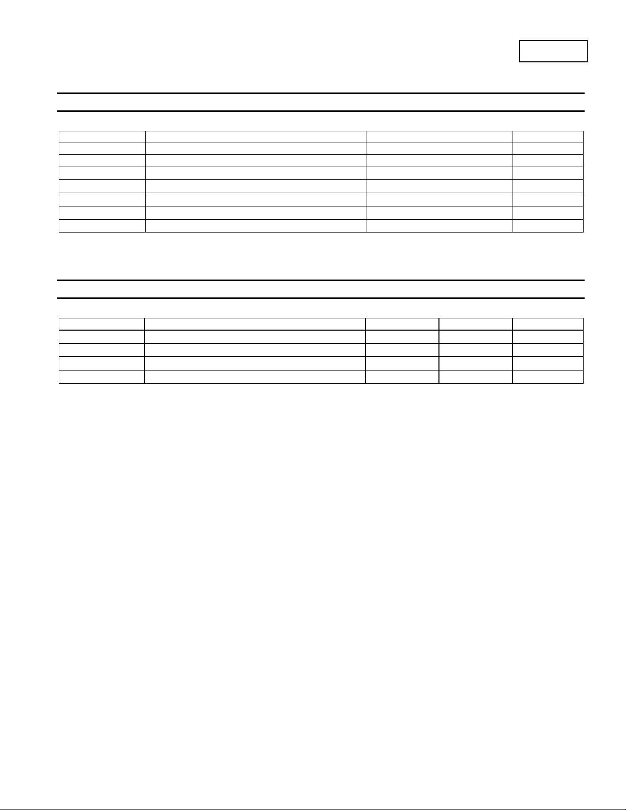
Absolute Maximum Ratings (cont.) (@T
Symbol Parameter Ratings Unit
ESD HBM Human Body Model ESD Protection 2000 V
ESD MM Machine Model ESD Protection 200 V
Input Voltage -0.3 to +6.0 V
OUT Voltage
Continuous Load Current Internal Limited
Storage Temperature Range -65 to +150 °C
Maximum Junction Temperature 150 °C
V
I
VIN
OUT
OUT
TST
TJ
Recommended Operating Conditions (@T
Symbol Parameter Min Max Unit
V
IN
I
OUT
T
A
TJ
Notes: 4. Stresses beyond those listed under Absolute Maximum Ratings may cause permanent damage to the device. These are stress ratings only and
functional operation of the device at these or any other conditions beyond those indicated are not implied. Exposure to absolute-maximum rated
conditions for extended periods may affect device reliability.
5. Operating junction temperature must be evaluated and derated as needed, based on ambient temperature (T
allowable operating junction temperature (T
Input voltage 2.2 5.5 V
Output Current 0 1.5 A
Operating Ambient Temperature -40 +85
Operating Junction Temperature (Note 5) -40 +125
= +25°C, unless otherwise specified.)
A
= +25°C, unless otherwise specified.)
A
), and package thermal resistance (θJA).
J-MAX
-0.3 to VIN +0.3
), power dissipation (PD), maximum
A
V
°C
°C
AP7363
Document number: DS35059 Rev. 8 - 2
3 of 14
www.diodes.com
December 2012
© Diodes Incorporated
Page 4
A
P7363
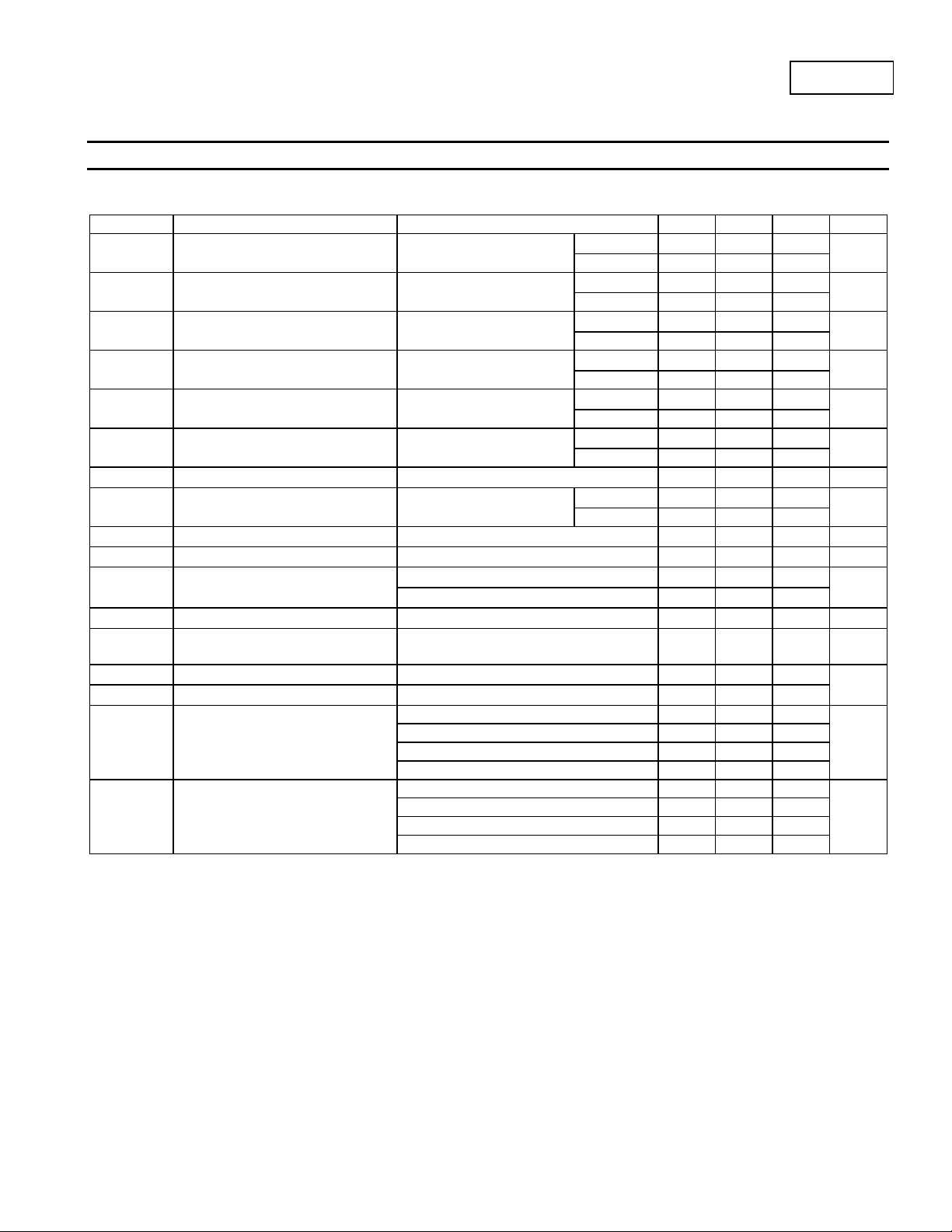
Electrical Characteristics (@T
Minimum and maximum limits are guaranteed through test, design, or statistical correlation. Typical values represent the most likely parametric
norm at T
V
ΔV
ΔV
Notes: 6. Dropout voltage is the minimum voltage difference between the input and the output at which the output voltage drops 2% below its nominal value.
For any output voltage less than 2.5V, the minimum V
7. The line and load regulation specification contains only the typical number. However, the limits for line and load regulation are included in the adjust
voltage tolerance specification.
8. Device mounted on 2” x 2” FR-4 substrate PCB, 2oz copper with minimum recommended pad layout.
= +25°C, and are provided for reference purposes only.
A
Symbol Parameter Test Conditions Min Typ Max Unit
V
ADJ
I
ADJ
DROPOUT
OUT
OUT
I
GND
I
OUT-PK
ISC
t
d(off)
t
d(on)
ADJ Pin Voltage
ADJ Pin Bias Current
Dropout Voltage (Note 6)
Line Regulation (Note 7)
/ΔVIN
Load Regulation (Note 7)
/ΔI
OUT
Ground Pin Current in Normal
Operation Mode
Peak Output Current
Short Circuit Current OUT grounded
Turn-Off Delay
Turn-On Delay
PSRR Ripple Rejection
ρ
T
SHDN
T
θ
θ
n(l/f)
en
HYS
Output Noise Density
Output Noise Voltage
Thermal Shutdown Threshold
Thermal Shutdown Hysteresis
Thermal Resistance Junction-to-
JA
Ambient
Thermal Resistance Junction-to-Case
JC
= +25°C, V
A
= 3.3V, I
IN
V
= V
IN
IN-MIN
= 10mA to 1.5A
I
OUT
VIN = V
IN-MIN
I
= 1.5A, V
OUT
VIN = V
IN-MIN
I
= 10mA to 1.5A
OUT
I
= 10mA to 1.5A
OUT
≥ V
V
OUT
OUT
to V
to V
OUT
to V
OUT - NOM
= 10mA, C
,
IN-MAX
IN-MAX
= 2.5V
IN-MAX
-5%
= 10µF, C
IN
T
A
= +25°C
= 10µF, unless otherwise specified.)
OUT
0.584 0.605 0.626
Over temp 0.575 0.635
T
= +25°C
A
50
Over temp 750
= +25°C
T
A
190 240
Over temp 280
T
= +25°C
A
— 0.04 —
Over temp 0.05
= +25°C
T
A
— 0.18 —
Over temp 0.33
T
= +25°C
A
1.0 1.2
Over temp 1.3
3.6
T
= +25°C
A
3.7
Over temp 2
From V
From V
V
IN
VIN = 3.0V, I
F = 120Hz, C
EN
EN
= 3.0V, I
< VIL to V
> VIH to V
OUT
OUT
= 1.5A, f = 120Hz
OUT
= 1.5A, f = 1kHz
OUT
= 10μF ceramic
OUT
BW = 100Hz – 100kHz,
= 10μF ceramic
C
OUT
T
rising
J
falling from T
T
J
SHDN
= OFF, I
= ON, I
OUT
OUT
= 1.5A
= 1.5A
25 μs
25 μs
65
61
1.0
100 μV(rms)
170
10
U-DFN2030-8 (Note 8) 174.0
SO-8EP (Note 8) 52.8
SOT223 (Note 8) 105.7
TO252 (Note 8) 87.8
U-DFN2030-8 (Note 8) 28.2
SO-8EP (Note 8) 10.0
SOT223 (Note 8) 18.5
TO252 (Note8) 17.3
operating voltage is the limiting factor.
IN
V
nA
mV
%/V
%/A
mA
A
A
dB
μV/√Hz
°C
o
C/W
o
C/W
AP7363
Document number: DS35059 Rev. 8 - 2
4 of 14
www.diodes.com
December 2012
© Diodes Incorporated
Page 5
A
k
)
2
5
D
R
O
P
OUT
OLT
G
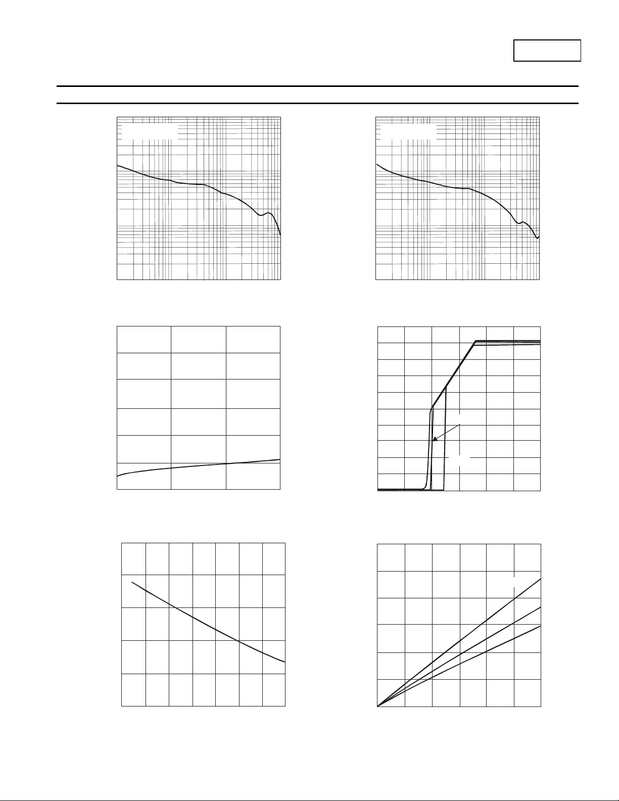
Typical Performance Characteristics (@T
10k
C = 10µF CER
OUT
= +25°C, VIN = 2.7V, C
J
10
= 10µF, C
IN
C = 10µF
OUT
OUT
= 10µF, I
= 10mA, V
OUT
OUT
P7363
= 1.8V.)
1k
√
100
NOISE (nV/ Hz)
10
100 1000 10k 100k
FREQUENCY (Hz)
Noise Density
3
2.5
2
1.5
GND
I (mA)
1
0.5
1k
√
NOISE (nV/ Hz)
100
10
100 1000 10k 100k
FREQUENCY (Hz)
125°C
Noise Density
25°C
-40°C
1
OUT
V (V
ADJ
V (V)
0
0.61
0.610
0.605
0.600
0
0.5 1 1.5
I (A)
LOAD
I vs. Load Current
GND
0
0123
Turn-On Characteristics
V (V)
IN
0.3
125°C
E (V)
0.2
A
25°C
V
-40°C
0.1
0.595
0.590
-50 -25 75 12502550 100
TEMPERATURE (°C)
V vs. Temperature
ADJ
0
00.5
LOAD CURRENT (A)
Dropout Voltage vs. Load Current
11.5
AP7363
Document number: DS35059 Rev. 8 - 2
5 of 14
www.diodes.com
December 2012
© Diodes Incorporated
Page 6
A
)
)
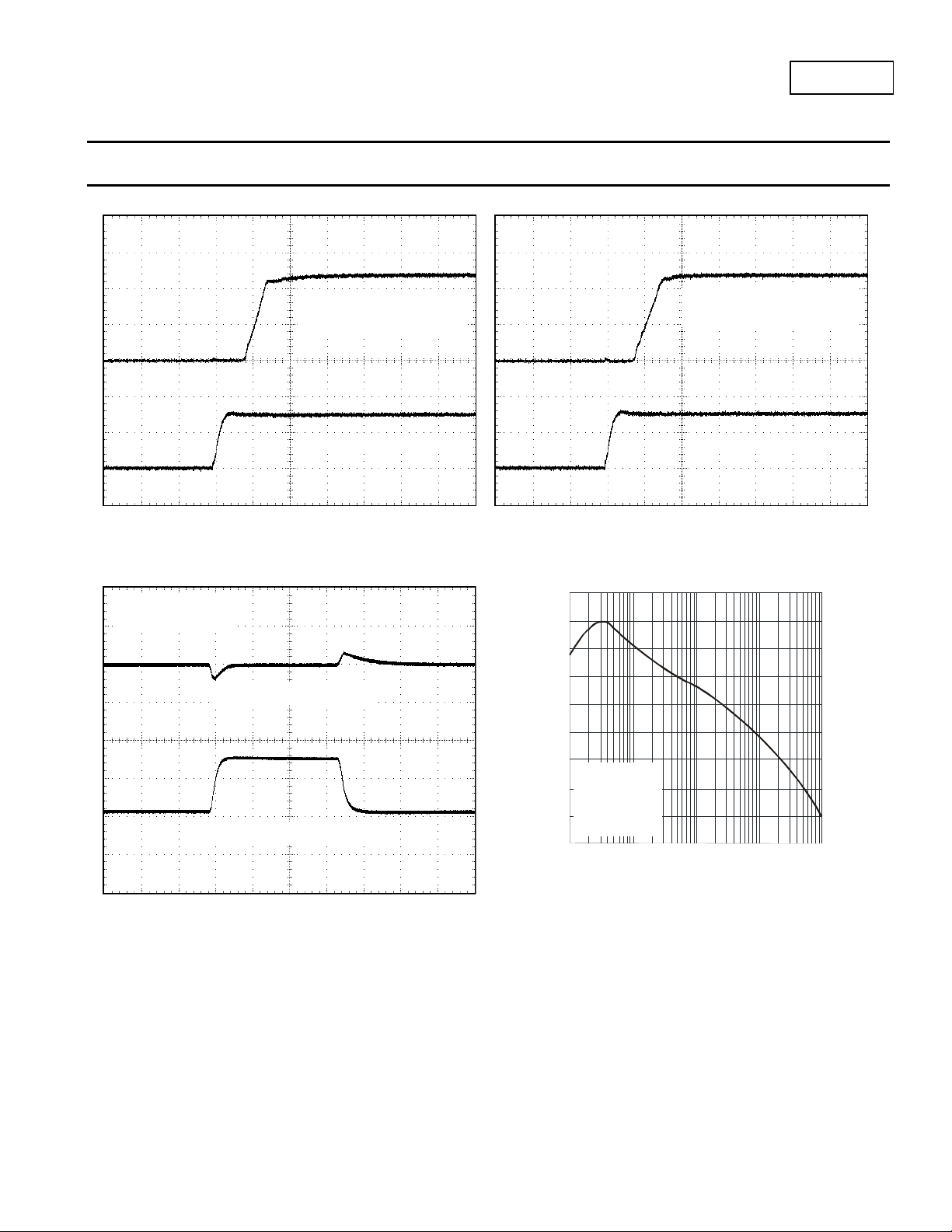
Typical Performance Characteristics (cont.)
(@TJ = +25°C, VIN = 2.7V, C
= 10µF, C
IN
OUT
Turn-On Time
V
OUT
I
= 0A, C
L
V
IN
= 10µF, I
= 1.2V (500mV/div)
OUT
= 10mA, V
OUT
= 10μF CER
= 3.0V (2V/div
OUT
= 1.8V.)
Turn-On Time
V
OUT
I
= 1.5A, C
L
V
= 3.0V (2V/div
IN
P7363
= 1.2V (500mV/div)
= 10μF CER
OUT
Time (10μs/div)
Time (10μs/div)
V
IN
C
OUT
= 3.3V
=10μF CER
Load Transient Response
90
80
70
60
V
= 1.8V (50mV/div)
OUT
50
40
30
V = 3.3V
IN
REJECTION RATIO (dB)
20
V = 1.8V
OUT
I
= 1A
OUT
C = 1µF CER
10
IN
C = 1µF CER
I
= 100mA to 1.5A (1A/div)
LOAD
OUT
0
100 1k 10k 100k 1M
FREQUENCY (kHz)
PSRR
Time (40μs/div)
AP7363
Document number: DS35059 Rev. 8 - 2
6 of 14
www.diodes.com
December 2012
© Diodes Incorporated
Page 7
A
P7363
Application Note
Input Capacitor
A minimum 2.2μF ceramic capacitor is recommended between IN and GND pins to decouple input power supply glitch and noise. The amount of
the capacitance may be increased without limit. Larger input capacitor like 10μF will provide better load transient response. This inpu t capacitor
must be located as close as possible to the device to assure input stability and reduce noise. For PCB layout, a wide copper trace is required for
both IN and GND pins. A lower ESR capacitor type allows the use of less capacitance, while higher ESR type requires more capacitance.
Output Capacitor
The output capacitor is required to stabilize and help the transient response of the LDO. The AP7363 is stable with any type of capacitor, with no
limitations on minimum or maximum ESR. The device is designed to have excellent transient response for most applications with a small amount
of output capacitance. The device is also stable with multiple capacitors in parallel, which can be of any type of value. Additional capacitance
helps to reduce undershoot and overshoot during transient loads. This capacitor sh ould be placed a s close as possible to OUT an d GND pins fo r
optimum performance.
Adjustable Operation
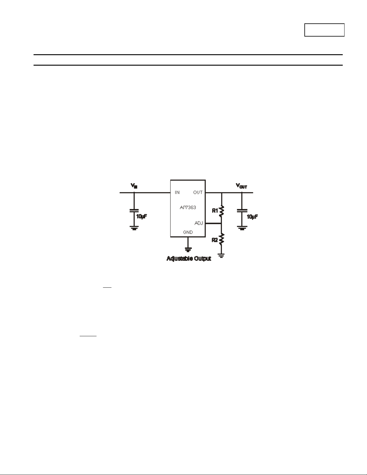
The AP7363 provides output voltage from 0.6V to 5.0V through external resistor divider as shown below.
The output voltage is calculated by:
⎛
⎜
V
OUT
Where V
Rearranging the equation will give the following that is used for adjusting the output to a particular voltage:
To maintain the stability of the internal reference voltage, R
REF
R
1
V
REF
⎜
⎝
= 0.6V (the internal reference voltage)
⎛
V
OUT
⎜
R
2
⎜
V
REF
⎝
⎞
R
1
⎟
+=
1
−= 1
⎟
R
2
⎠
⎞
⎟
⎟
⎠
need to be kept smaller than 10kΩ.
2
No Load Stability
Other than external resistor divider, no minimum load is required to keep the device stable. The device will remain stable and regulated in no
load condition.
AP7363
Document number: DS35059 Rev. 8 - 2
7 of 14
www.diodes.com
December 2012
© Diodes Incorporated
Page 8
A
OOP G
OOP GAIN
P7363
Application Note (cont.)
Stability and Phase Margin
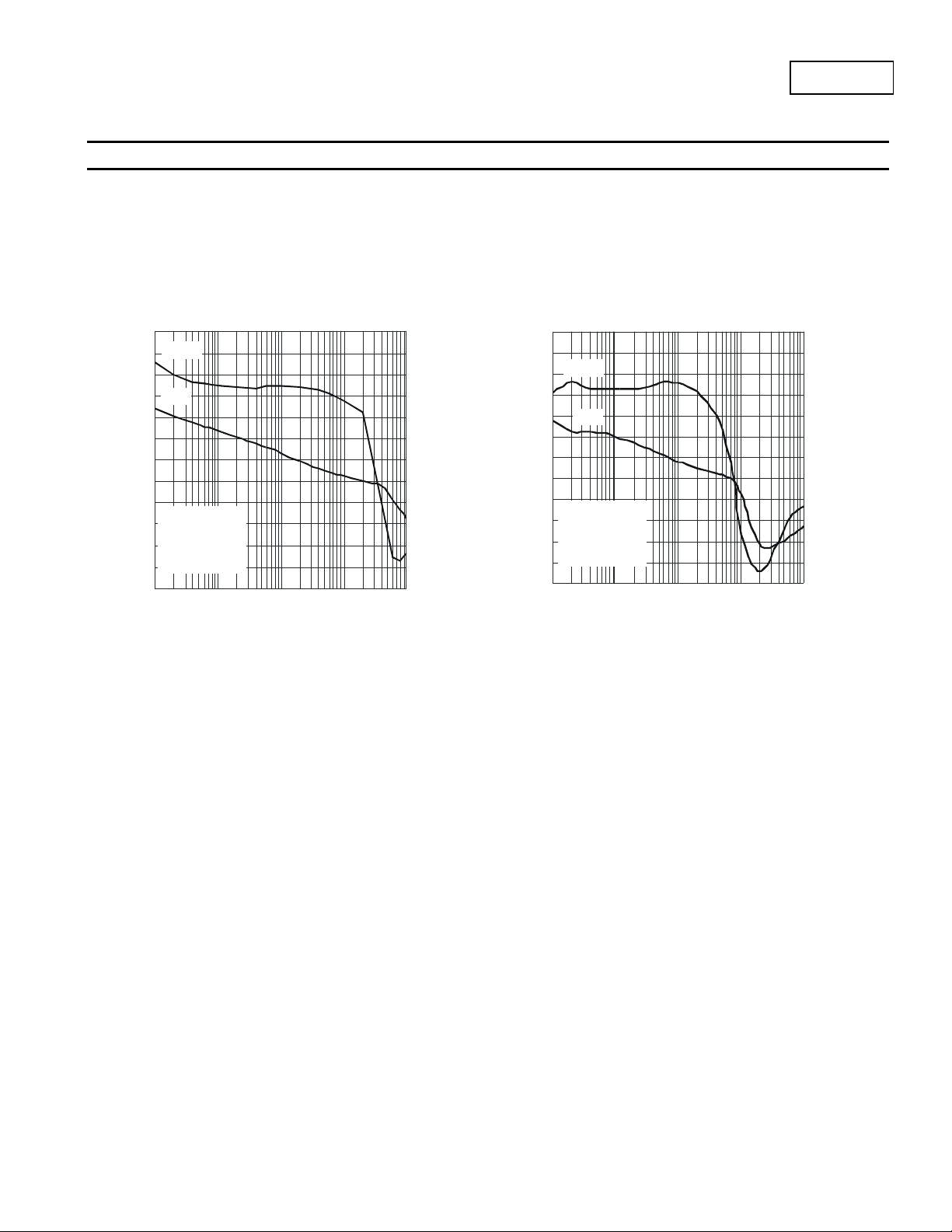
Any regulator which operates using a feedback loop must be compensated in such a way as to ensure adequate phase margin, which is defined
as the difference between the phase shift and -180 degrees at the frequency where the loop gain cr osses unity (0 dB ). For most LD O regulators,
the ESR of the output capacitor is required to create a zero to add enough phase lead to ensure stable operation. The AP7363 has a internal
compensation circuit which maintains phase margin regardless of the ESR of the output capacitor, any type of capacitos can be used.
The two charts on the next page show the gain/phase plot of the AP7363 with an output of 1.2V, 10 μF ceramic output capacitor, delivering 1.5A
load current and no load. It can be seen the phase margin is about 90° (which is very stable).
120
100
AIN (dB)
-20
L
-40
-60
-80
-100
-120
80
60
40
20
0
100
PHASE
GAIN
V = 2.7V
IN
V = 1.2V
OUT
I = 1.5A
L
C = 10µF CER
OUT
1k 10k 100k 1M
140
120
100
80
60
40
20
0
-20
-40
-60
-80
PHASE MARGIN (°)
FREQUENCY(Hz)
Gain-Bandwidth Plot for 1.5A Load
Short Circuit Protection
When output current at OUT pin is higher than current limit threshold, the current limit protection will be triggered and clamp the output current to
prevent over-current and to protect the regulator from damage due to overheating.
Thermal Shutdown Protection
Thermal protection disables the output when the junction temperature rises to approximately +170°C, allowing the device to cool down. When the
junction temperature reduces to approximately +160°C the output circuitry is enabled again. Depending on power dissipation, thermal resistance,
and ambient temperature, the thermal protection circuit may cycle on and off. This cycling limits the heat dissipation of the regulator, protecting it
from damage due to overheating.
Low Quiescent Current
The AP7363, consuming only around 0.5mA for all input range, provides great power saving in portable and low power applications.
Output Noise
This is the integrated value of the output noise over a specified frequency range. Input voltage and output load current are kept constant during
the measurement. Results are expressed in µVrms or µV√Hz.
The AP7363 is a low noise regulator and needs no external noise reduction capacitor. Output voltage noise is typically 100μVrms overall noise
level between 100 Hz and 100 kHz.
120
100
PHASE
80
60
40
(dB)
GAIN
20
0
-20
L
-40
V = 2.7V
IN
-60
V = 1.2V
OUT
I = 0A
-80
L
C = 10µF CER
-100
OUT
-120
100 1k 10k 100k 1M
FREQUENCY(Hz)
Gain-Bandwidth Plot for no Load
140
120
100
80
60
40
20
0
-20
-40
-60
-80
PHASE MARGIN (°)
Noise is specified in two ways:
Output noise density is the RMS sum of all noise sources, measured at the regulator output, at a specific frequency (measured with a 1Hz
bandwidth). This type of noise is usually plotted on a curve as a function of frequency.
Output noise voltage is the RMS sum of spot noise over a specified bandwidth. Spot noise is measured in units μV/√Hz or nV/√Hz and total
output noise is measured in μV(rms). The primary source of noise in low-dropout regulators is the internal reference.
AP7363
Document number: DS35059 Rev. 8 - 2
8 of 14
www.diodes.com
December 2012
© Diodes Incorporated
Page 9
A
P7363
Application Note (cont.)
Power Dissipation
The device power dissipation and proper sizing of the thermal plane that is connected to the thermal pad is critical to avoid thermal shutdown and
ensure reliable operation. Power dissipation of the device depends on input voltage and load conditions and can be calculated by:
P
The maximum power dissipation, handled by the device, depends on the junction to ambient thermal resistance, and maximum ambient
temperature, which can be calculated by the equation in the following:
= (V
- V
D
IN
P
max_D
) X I
OUT
OUT
=
°+
R
θ
JA
)AT-C150(
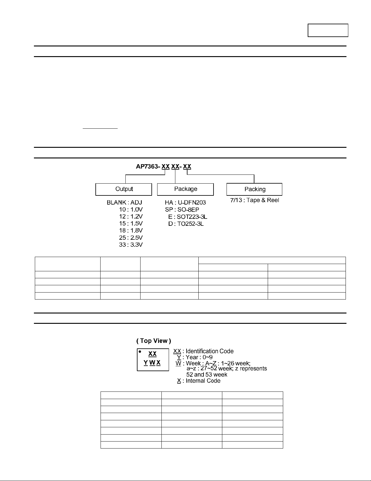
Ordering Information
Part Number Package Code
AP7363-XXHA-7 HA U-DFN2030-8 3000/Tape & Reel -7
AP7363-XXSP-13 SP SO-8EP 2500/Tape & Reel -13
AP7363-XXE-13 E SOT223-3L 2500/Tape & Reel -13
AP7363-XXD-13 D TO252-3L
Note: 9. TO252 and SOT223 are only available with fixed output version.
Packaging
(Note 9)
Quantity Part Number Suffix
2500/Tape & Reel
7”/13” Tape and Reel
Marking Information
(1) U-DFN2030-8
AP7363
Document number: DS35059 Rev. 8 - 2
Device Package Identification Code
AP7363ADJ U-DFN2030-8 SA
AP7363-10 U-DFN2030-8 SB
AP7363-12 U-DFN2030-8 SC
AP7363-15 U-DFN2030-8 SD
AP7363-18 U-DFN2030-8 SE
AP7363-25 U-DFN2030-8 SF
AP7363-33 U-DFN2030-8 SG
9 of 14
www.diodes.com
-13
December 2012
© Diodes Incorporated
Page 10
A
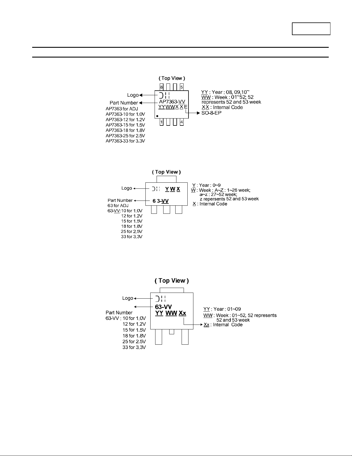
Marking Information (cont.)
(2) SO-8EP
P7363
(3) SOT223
(4) TO252
AP7363
Document number: DS35059 Rev. 8 - 2
10 of 14
www.diodes.com
December 2012
© Diodes Incorporated
Page 11
A
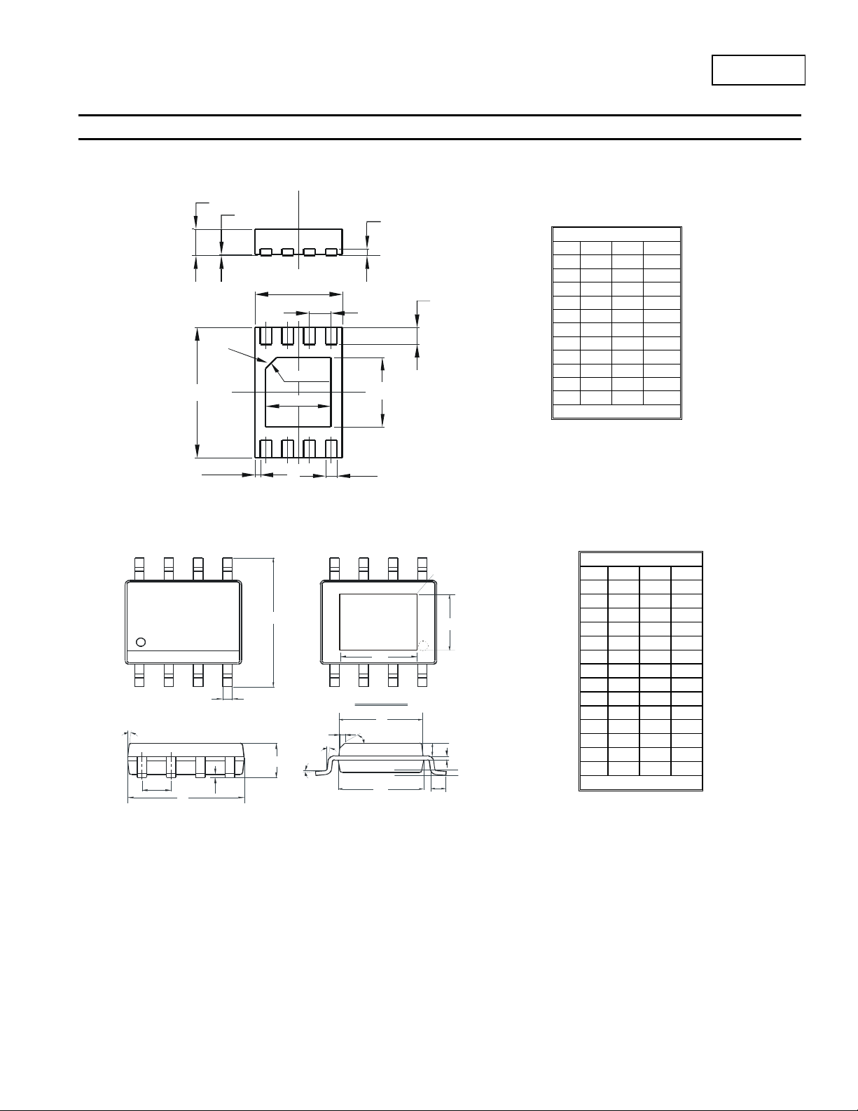
Package Outline Dimensions (All dimensions in mm.)
Please see AP02002 at http://www.diodes.com/datasheets/ap02002.pdf for latest version.
(1) U-DFN2030-8
A
A1
D
e
(Pin #1 ID)
E
Z
C'0.25*45°
D2
A3
Seating Plane
E2
b
L
(2) SO-8EP
85
E1
14
F
Exposed Pad
H
A1
b
4° ± 3°
A
7
°
Bottom View
N
E
45
°
E0
Q
C
L
Gauge Plane
Seating Plane
9° (All si de s)
e
D
AP7363
Document number: DS35059 Rev. 8 - 2
11 of 14
www.diodes.com
U-DFN2030-8
Dim Min Max Typ
A 0.57 0.63 0.60
A1 0 0.05 0.02
A3 - - 0.15
b 0.20 0.30 0.25
D 1.95 2.05 2.00
D2 1.40 1.60 1.50
e - - 0.50
E 2.95 3.05 3.00
E2 1.50 1.70 1.60
L 0.35 0.45 0.40
Z - - 0.125
All Dimensions in mm
SO-8EP (SOP-8L-EP)
Dim Min Max Typ
A 1.40 1.50 1.45
A1 0.00 0.13 -
b 0.30 0.50 0.40
C 0.15 0.25 0.20
D 4.85 4.95 4.90
E 3.80 3.90 3.85
E0 3.85 3.95 3.90
E1 5.90 6.10 6.00
e - - 1.27
F 2.75 3.35 3.05
H 2.11 2.71 2.41
L 0.62 0.82 0.72
N - - 0.35
Q 0.60 0.70 0.65
All Dimensions in mm
P7363
December 2012
© Diodes Incorporated
Page 12
A
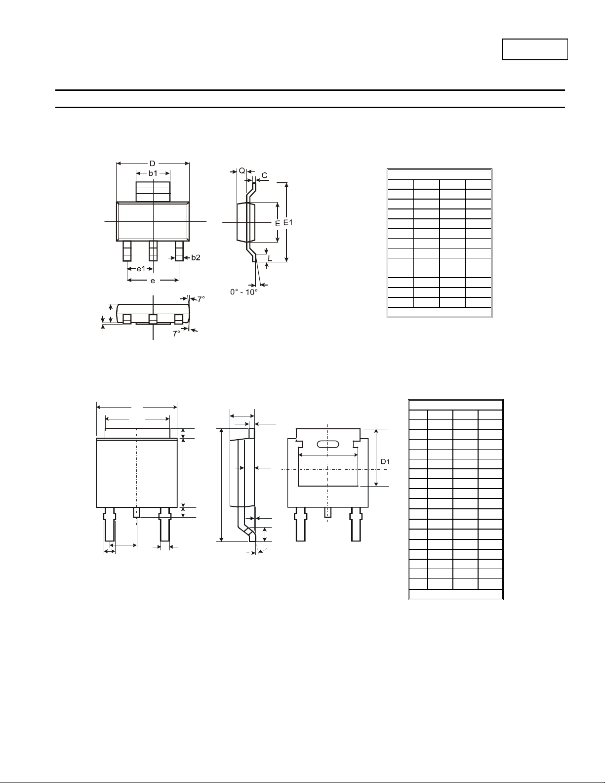
Package Outline Dimensions (cont.) (All dimensions in mm.)
Please see AP02002 at http://www.diodes.com/datasheets/ap02002.pdf for latest version.
(3)
SOT223
A
c2
A2
H
L4
A1
L
a
E1
(4)
TO252
A
A1
2X b2
E
b3
L3
D
e
3X b
Dim Min Max Typ
SOT223
A 1.55 1.65 1.60
A1 0.010 0.15 0.05
b1 2.90 3.10 3.00
b2 0.60 0.80 0.70
C 0.20 0.30 0.25
D 6.45 6.55 6.50
E 3.45 3.55 3.50
E1 6.90 7.10 7.00
e — — 4.60
e1 — — 2.30
L 0.85 1.05 0.95
Q 0.84 0.94 0.89
All Dimensions in mm
Dim Min Max Typ
A1 0.00 0.13 0.08
A2 0.97 1.17 1.07
b2 0.76 1.14 0.95
b3 5.21 5.46 5.33
c2 0.45 0.58 0.531
D1 5.21
E1 4.32
L3 0.88 1.27 1.08
L4 0.64 1.02 0.83
All Dimensions in mm
TO252
A 2.19 2.39 2.29
b 0.64 0.88 0.783
D 6.00 6.20 6.10
− −
e
− −
E 6.45 6.70 6.58
H 9.40 10.41 9.91
L 1.40 1.78 1.59
a 0° 10°
2.286
− −
−
P7363
AP7363
Document number: DS35059 Rev. 8 - 2
12 of 14
www.diodes.com
December 2012
© Diodes Incorporated
Page 13
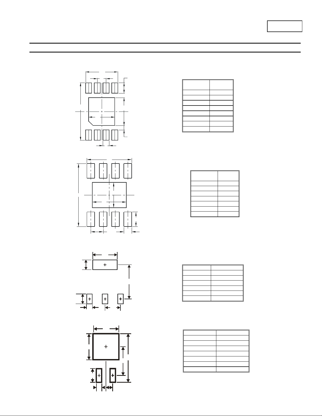
A
Suggested Pad Layout
Please see AP02001 at http://www.diodes.com/datasheets/ap02001.pdf for the latest version.
(1) U-DFN2030-8
(2) SO-8EP
Y2
Pin1
X1
X2
C
X
X2
Y
Y1
G
Dimensions
C 0.500
G 0.250
X 0.350
X1 1.500
X2 1.850
Y 0.600
Y1 1.600
Y2 3.300
Y2
(3) SOT223
Y1
Y2
X2
(4) TO252
Y2
AP7363
Document number: DS35059 Rev. 8 - 2
Y1
X1
X1
X1
X2
C
E1
C2
Y1
Y
X
C1
Z
C
13 of 14
www.diodes.com
Dimensions
Dimensions Value (in mm)
X1 3.3
X2 1.2
Y1 1.6
Y2 1.6
C1 6.4
C2 2.3
Dimensions Value (in mm)
Z 11.6
X1 1.5
X2 7.0
Y1 2.5
Y2 7.0
C 6.9
E1 2.3
Value
(in mm)
Value
(in mm)
C 1.270
X 0.802
X1 3.502
X2 4.612
Y 1.505
Y1 2.613
Y2 6.500
P7363
December 2012
© Diodes Incorporated
Page 14

A
P7363
DIODES INCORPORATED MAKES NO WARRANTY OF ANY KIND, EXPRESS OR IMPLIED, WITH REGARDS TO THIS DOCUMENT,
INCLUDING, BUT NOT LIMITED TO, THE IMPLIED WARRANTIES OF MERCHANTABILITY AND FITNESS FOR A PARTICULAR PURPOSE
(AND THEIR EQUIVALENTS UNDER THE LAWS OF ANY JURISDICTION).
Diodes Incorporated and its subsidiaries reserve the right to make modifications, enhancements, improvements, corrections or other changes
without further notice to this document and any product described herein. Diodes Incorporated does not assume any liability arising out of the
application or use of this document or any product described herein; neither does Diodes Incorporated convey any license under its patent or
trademark rights, nor the rights of others. Any Customer or user of this document o r products described herein in such applica tions shall assume
all risks of such use and will agree to hold Diodes Incorporated and all the companies whose products are represented on Diodes Incorporated
website, harmless against all damages.
Diodes Incorporated does not warrant or accept any liability whatsoever in respect of any products purchased through unauthorized sales channel.
Should Customers purchase or use Diodes Incorporated products for any unintended or unauthorize d application, Customers shall indemnify and
hold Diodes Incorporated and its representatives harmless against all claims, damages, expenses, and attorney fees arising out of, directly or
indirectly, any claim of personal injury or death associated with such unintended or unauthorized application.
Products described herein may be covered by one or more United States, international or foreign patents pending. Product names and markings
noted herein may also be covered by one or more United States, international or foreign trademarks.
This document is written in English but may be translated into multiple languages for reference. Onl y the English version of this document is the
final and determinative format released by Diodes Incorporated.
Diodes Incorporated products are specifically not authorized for use as critical components in life support devices or systems without the express
written approval of the Chief Executive Officer of Diodes Incorporated. As used herein:
A. Life support devices or systems are devices or systems which:
1. are intended to implant into the body, or
2. support or sustain life and whose failure to perform when properly used in accordance with instructions for use provided in the
labeling can be reasonably expected to result in significant injury to the user.
B. A critical component is any component in a life support device or system whose failure to perform can be reasonably expected to cause the
failure of the life support device or to affect its safety or effectiveness.
Customers represent that they have all necessary expertise in the safety and regulatory ramifications of their life support devices or systems, and
acknowledge and agree that they are solely responsible for all legal, regulatory and safety-related requirements concerning their products and any
use of Diodes Incorporated products in such safety-critical, life support devices or systems, notwithstanding any devices- or systems-related
information or support that may be provided by Diodes Incorporated. Further, Customers must fully indemnify Diodes Incorporated and its
representatives against any damages arising out of the use of Diodes Incorporated products in such safety-critical, life support devices or systems.
Copyright © 2012, Diodes Incorporated
www.diodes.com
IMPORTANT NOTICE
LIFE SUPPORT
AP7363
Document number: DS35059 Rev. 8 - 2
14 of 14
www.diodes.com
December 2012
© Diodes Incorporated
 Loading...