

Page 1
AP7333
300mA, Low Quiescent Current, Fast Transient
Low Dropout Linear Regulator
Features
• 300mA Low Dropout Regulator in 3-pin package
• Very low I
• Wide input voltage range: 2V to 6V
• Fixed output options: 1.0V to 3.3V
• PSRR: 65dB typical at 100Hz
• Fast start-up time: 80µs
• Stable with low ESR, 1µF ceramic output capacitor
• Excellent Load/Line Transient Response
• Low dropout: 300mV typical at 300mA
• Current limit protection
• Short circuit protection
• Thermal shutdown protection
• Ambient temperature range: -40ºC to 85°C
• SOT23 and SOT23R: Available in “Green” Molding
Compound (No Br, Sb)
• Lead Free Finish/RoHS Compliant (Note 1)
over full load: 65µA
Q
Applications
• XDSL Router
• Wireless LAN Cards
• Desktop and Notebook Computers
• Battery Powered Equipments
• Mouse, Keyboards
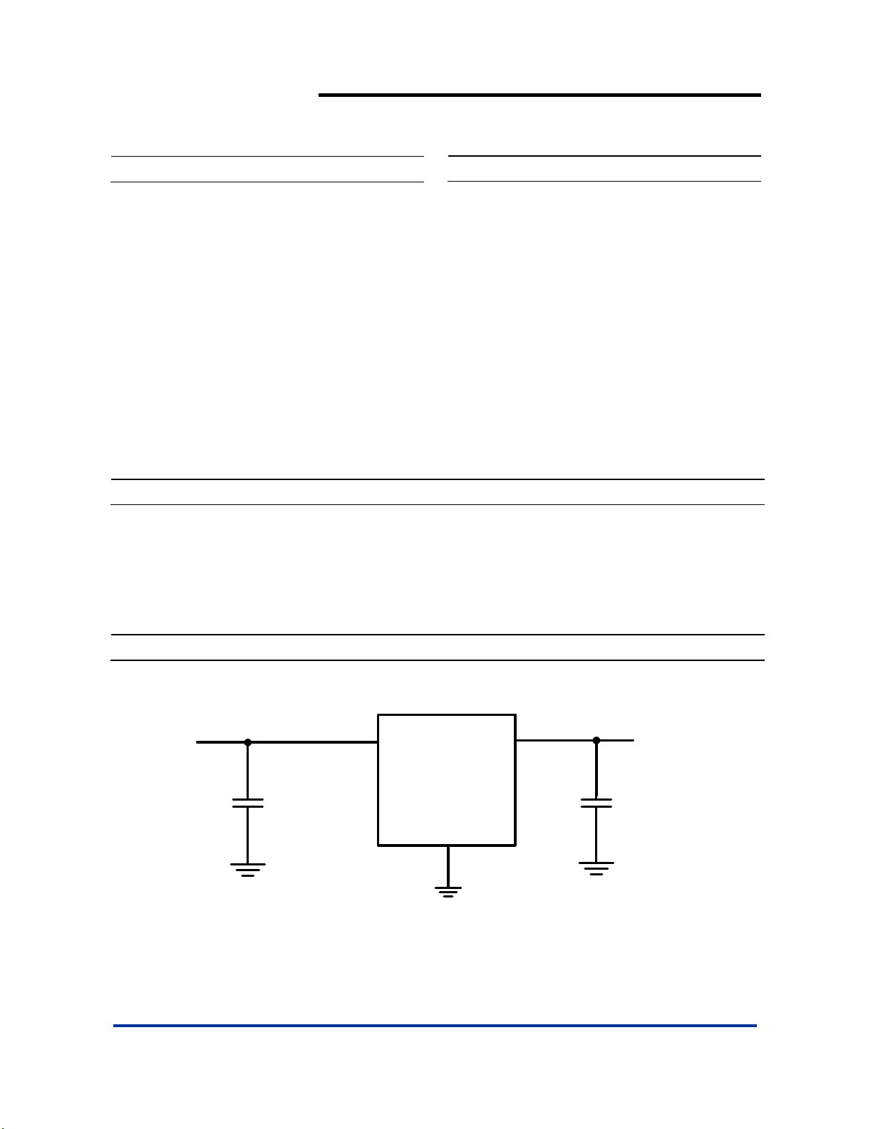
Typical Application Circuit
Description
The AP7333 is a 300mA, fixed output voltage, low dropout linear
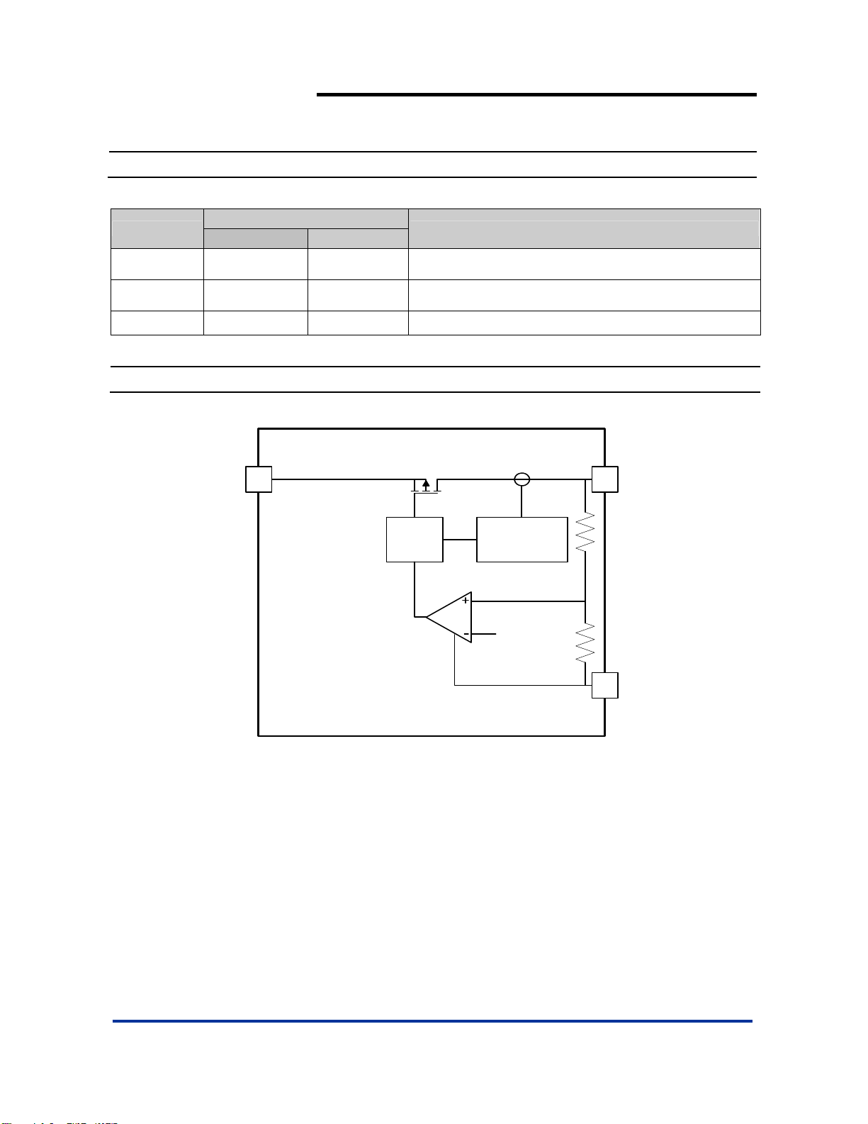
regulator. The device included pass element, error amplifier,
band-gap, current limit and thermal shutdown circuitry.
The characteristics of low dropout voltage and low quiescent
current make it suitable for low power applications, for example,
battery powered devices. The typical quiescent current is
approximately 65μA.
Built-in current-limit and thermal-shutdown functions prevent IC
from damage in fault conditions.
The AP7333 is available in SOT23 packages with different
pin-outs.
V
IN
IN
OUT
V
OUT
AP7333
1uF
1uF
GND
AP7333 Rev. 2 1 of 12 NOVEMBER 2009
www.diodes.com © Diodes Incorporated
Page 2
Ordering Information
AP7333
300mA, Low Quiescent Current, Fast Transient
Low Dropout Linear Regulator
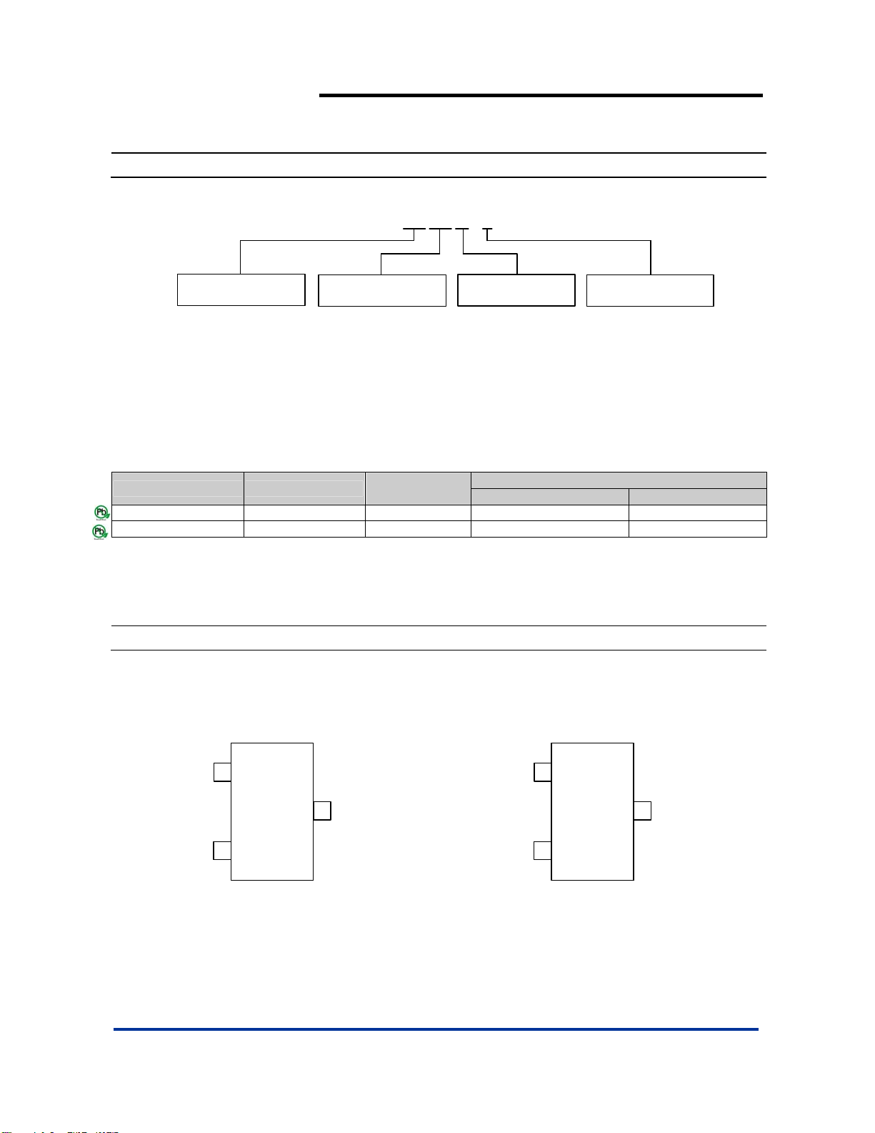
AP7333 - XX XX G - 7
Output
10 : 1.0V
12 : 1.2V
Package Green
SA : SOT23
G : Green
SR : SOT23R
Packing
7 : Tape & Reel
15 : 1.5V
18 : 1.8V
20 : 2.0V
25 : 2.5V
28 : 2.8V
30 : 3.0V
33 : 3.3V
Device Package Code
AP7333-XXSAG-7 SA SOT23 3000/Tape & Reel -7
AP7333-XXSRG-7 SR SOT23R 3000/Tape & Reel -7
Notes: 1. EU Directive 2002/95/EC (RoHS). All applicable RoHS exemptions applied. Please visit o ur website at
http://www.diodes.com/datasheets/ap02001.pdf.
http://www.diodes.com/products/lead_free.html
2. Pad layout as shown on Diodes Inc. suggested pad layout document AP02001, which can be found on our website at
Packaging
(Note 2)
7” Tape and Reel
Quantity Part Number Suffix
Pin Assignment
(1) SOT23 (1) SOT23R
IN
OUT
( Top View )
1
2
3
GND
GND
OUT
( Top View )
1
2
3
IN
AP7333 Rev. 2 2 of 12 NOVEMBER 2009
www.diodes.com © Diodes Incorporated
Page 3
300mA, Low Quiescent Current, Fast Transient
Pin Descriptions
Pin Name
IN 1 3
OUT 2 2
GND 3 1 Ground
Functional Block Diagram
Pin Number
SOT23 SOT23R
Voltage input pin. Bypass to ground through at least 1µF
capacitor
Voltage output pin. Bypass to ground through 1µF ceramic
capacitor
AP7333
Low Dropout Linear Regulator
Description
IN
Gate
Driver
Current Lim it
and Thermal
Shutdown
V
REF
OUT
R
R
GND
AP7333 Rev. 2 3 of 12 NOVEMBER 2009
www.diodes.com © Diodes Incorporated
Page 4
AP7333
300mA, Low Quiescent Current, Fast Transient
Low Dropout Linear Regulator
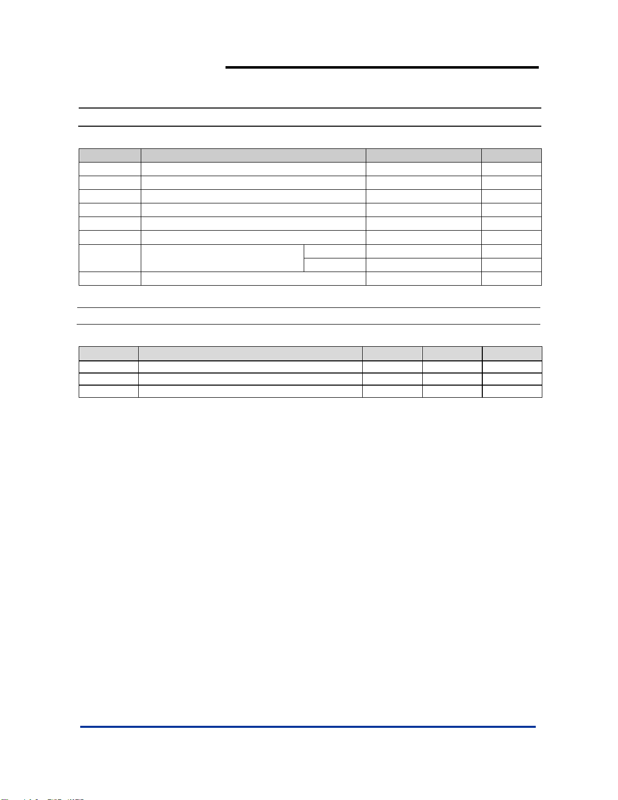
Absolute Maximum Ratings
Symbol Parameter Ratings Units
ESD HBM Human Body Model ESD Protection 6 kV
ESD MM Machine Model ESD Protection 400 V
VIN Input Voltage 7 V
Continuous Load Current Internal Limited
TOP Operating Junction Temperature Range -40 ~ 125 °C
TST Storage Temperature Range -65 ~150 °C
PD Power Dissipation (Note 3)
TJ Maximum Junction Temperature 150 °C
SOT23 600 mW
SOT23R 540 mW
Recommended Operating Conditions
Symbol Parameter Min Max Unit
V
IN
I
OUT
T
A
Notes: 3. Ratings apply to ambient temperature at 25°C
4. The device maintains a stable, regulated output voltage without a load current.
Input voltage 2 6 V
Output Current (Note 4) 0 300 mA
Operating Ambient Temperature -40 85
°C
AP7333 Rev. 2 4 of 12 NOVEMBER 2009
www.diodes.com © Diodes Incorporated
Page 5
⎯
AP7333
300mA, Low Quiescent Current, Fast Transient
Low Dropout Linear Regulator
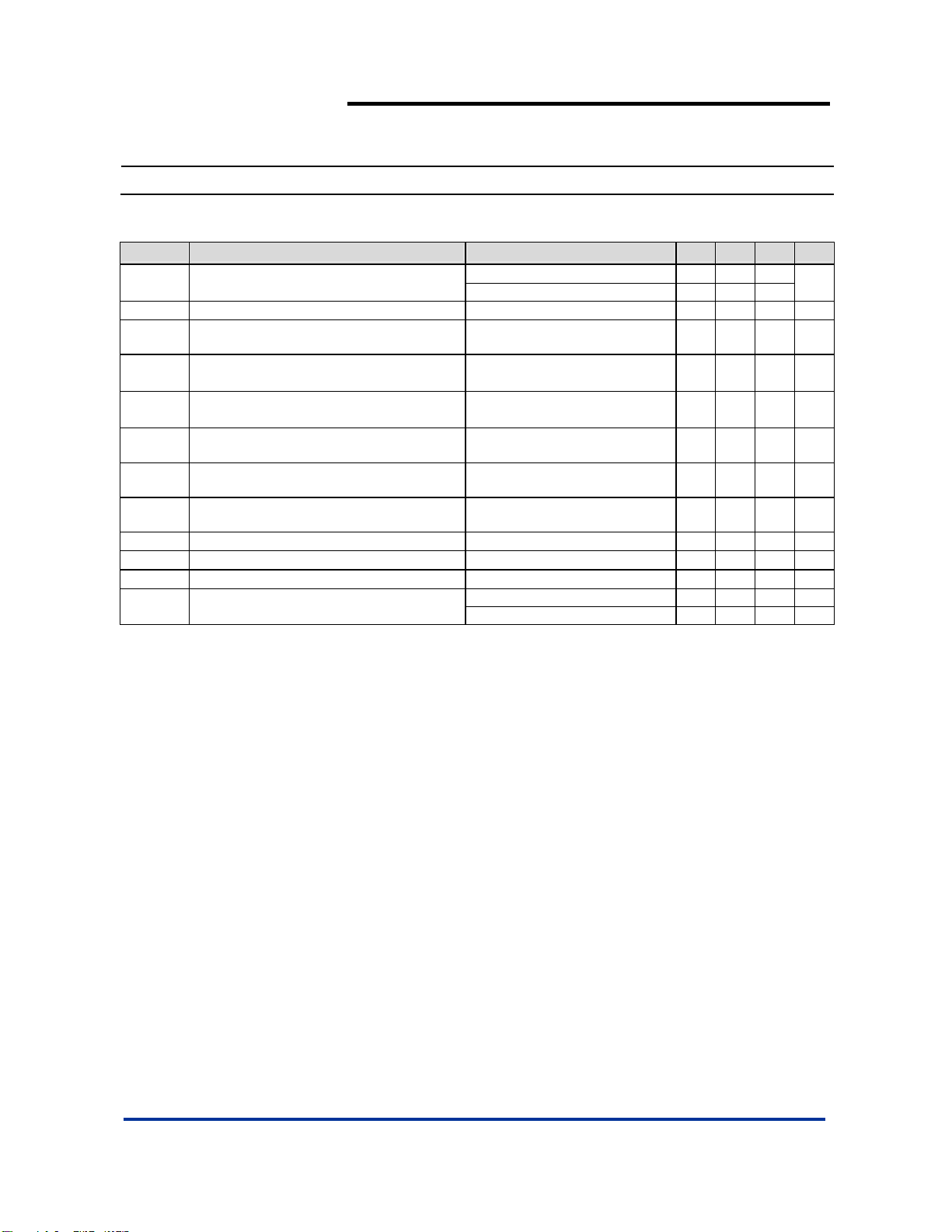
Electrical Characteristics
(TA = 25oC, V
Symbol Parameter Test Conditions Min Typ. Max Unit
I
V
Dropout
V
OUT
ΔV
/ΔV
ΔV
/V
tST
PSRR
I
SHORT
I
LIMIT
T
SHDN
T
HYS
θ
Notes: 5. Dropout voltage is the voltage difference between the input and the output at which the output voltage drops 2% below its nominal value.
This parameter only applies to output voltages above 1.8V.
6. Test conditions for SOT23 and SOT23R: Device mounted on FR-4 substrate PCB, with minimum recommended pad layout, 2oz copper, single
sided.
= V
+1V, C
IN
OUT
Input Quiescent Current
Q
Dropout Voltage (Note 5) I
Output Voltage Accuracy
OUT
Line Regulation
/V
IN
OUT
Load Regulation
OUT
Start-up Time
PSRR
Short-circuit Current
Current Limit V
= 1uF, C
IN
= 1uF, unless otherwise stated)
OUT
= 0mA
I
OUT
I
= 300mA 65 85
OUT
= 300mA 300 550 mV
OUT
T
= -40oC to 85oC,
A
I
= 30mA
OUT
= (V
V
IN
= 1mA
I
OUT
V
= (V
IN
I
from 1mA to 300mA
OUT
V
= 0V to 2.0V, V
IN
= 300mA
I
OUT
V
= [V
IN
f = 100Hz, I
V
= V
IN
V
OUT
OUT/ROUT
+1V) to V
OUT
+1V) to V
OUT
+1V]VDC + 0.5V
OUT
= 30mA
OUT
to V
IN-Min
IN-Max
OUT
IN-Max
IN-Max
= 1V,
,
,
,
ppAC
< 0.2V
= 1A 400 600 mA
-2 2 %
0.01 0.20 %/V
-0.6 0.6 %
80 μs
,
65 dB
100 mA
Thermal Shutdown Threshold 140
Thermal Shutdown Hysteresis 15
Thermal Resistance Junction-to-Ambient
JA
SOT23 (Note 6) 207
SOT23R (Note 6) 230 oC/W
55 75
μA
°C
°C
o
C/W
AP7333 Rev. 2 5 of 12 NOVEMBER 2009
www.diodes.com © Diodes Incorporated
Page 6
300mA, Low Quiescent Current, Fast Transient
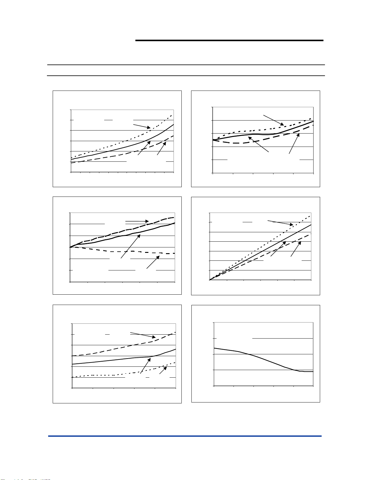
Typical Performance Characteristics
Quiescent Curr ent vs Input Voltage
60
Vout=2.5V
58
56
54
52
Outp u t Cu rr ent (mA)
50
48
2.7 3 3.3 3.6 3.9 4.2 4.5 4.8 5.1 5.4 5.7 6
Iload=0mA
90℃
25℃ -45℃
Input Voltage (V)
AP7333
Low Dropout Linear Regulator
Line Regulation (%/V)
0.1
0.06
0.02
-0.02
-0.06
Output Voltage Variation (%/V)
-0.1
3.5 4 4.5 5 5.5 6
Vout=2.5V
V
90℃
in=Vout +1V
Input Voltage (V)
25℃
-45℃
Load Regulati on (%)
0.6
0.4
0.2
0
-0.2
Vout=2.5V
-0.4
Output V o ltage Variation (%)
in=Vout +1V
V
-0.6
0 50 100 150 200 250 300
-45℃
25℃
90℃
Output Current (mA)
350
Vout=2.5V
300
250
200
150
100
Dropout Voltage (mV)
50
0
0 50 100 150 200 250 300
Dropout Vol tage
90℃
25℃
Output Cu rr ent (m A)
-45℃
Short Ci rc ui t vs I nput Vol t a ge
105
Vout=2.5V
100
95
90
85
Outpu t Cu r re n t (mA)
80
75
3.5 4 4.5 5 5.5 6
-45℃
25℃
Input Voltage (V)
Current Limit (mA)
90℃
Current Limit vs Input Voltage
600
Ta=25℃
out=2.5V
V
550
500
450
400
3.5 4 4.5 5 5.5 6
Input Voltage (V)
AP7333 Rev. 2 6 of 12 NOVEMBER 2009
www.diodes.com © Diodes Incorporated
Page 7
300mA, Low Quiescent Current, Fast Transient
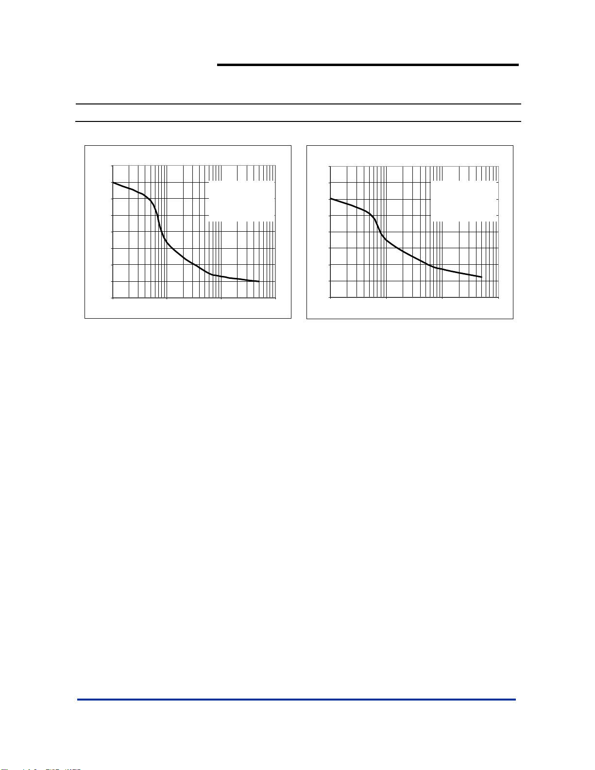
Typical Performance Characteristics (Continued)
AP7333
Low Dropout Linear Regulator
75
70
65
60
55
PS RR (d B)
50
45
40
35
0.1 1 10 100
PSRR
Vout=1V
Vin=2V
Cin=Cout=1uF
Ta=25℃
Frequency (kHz)
75
70
65
60
55
PS RR (d B)
50
45
40
35
0.1 1 10 100
PSRR
Vout=2.5V
Vin=3.5V
Cin=Cout=1uF
Ta=25℃
Freque ncy (kHz)
Line Transient Response
Vin=2V to 3V (1V/div)
Tr=10us
Vout=1V (50mV/div)
Line Transient Response
Vin=3V to 2V (1V/div)
Tr=10us
Vout=1V (50mV/div)
Iout=300mA (300mA/div)
Time (50us/div)
Time (50us/div)
Iout=300mA (300mA/div)
AP7333 Rev. 2 7 of 12 NOVEMBER 2009
www.diodes.com © Diodes Incorporated
Page 8

300mA, Low Quiescent Current, Fast Transient
Typical Performance Characteristics (Continued)
Tr=Tf=10us
Vin=2V
Load Transient Response
Tr=Tf=10us
Vin=3.5V
Vout=1V
(100mV/div)
Load Transient Response
AP7333
Low Dropout Linear Regulator
Vout=2.5V
(100mV/div)
Iout=1mA to 300mA
(100mA/div)
Iout=1mA to 300mA
(100mA/div)
Time (200us/div)
Time (200us/div)
Start-Up Time (No Load)
Vin=0 to 3.5V (1V/div)
Cin=Cout=1uF
Vout=2.5V (1V/div)
Time (50us/div)
Start-Up Time (300mA Load)
Vin=0 to 3.5V (1V/div)
Cin=Cout=1uF
Vout=2.5V (1V/div)
Iout (300mA/div)
Time (50us/div)
AP7333 Rev. 2 8 of 12 NOVEMBER 2009
www.diodes.com © Diodes Incorporated
Page 9

300mA, Low Quiescent Current, Fast Transient
Application Note
Input Capacitor
A 1μF ceramic capacitor is recommended to connect between
and GND pins to decouple input power supply glitch and
V
IN
noise. The amount of the capacitance may be increased
without limit. This i nput capacitor must be located as close as
possible to the device to assure input stability and less noise.
For PCB layout, a wide copper trace is required for both V
GND. A lower ESR capacitor allows the use of less
capacitance, while higher ESR type requires more
capacitance.
Output Capacitor
The output capacitor is required to stabilize and help transient
response for LDO. The AP7333 is stable with very small
ceramic output capacitors. The recommended capacitance is
from 1μF to 4.7μF, Equivalent Series Resistance (ESR) is from
10mΩ to 200mΩ, and temperature characteristic is X7R or X5R.
Higher capacitance values help to improve load/line transient
response. The output capacitance may be increased to keep
low undershoot/overshoot. Place output capacitor as close as
possible to OUT and GND pins, and keep the leads as short as
possible.
No Load Stability
No minimum load is required to keep the device stable. The
device will remain stable and regulated in no load condition.
Current Limit Protection
When output current at OUT pin is higher than current limit
threshold, the current limit protection will be triggered and
clamp the output current to approximately 600mA to prevent
over-current and to protect the regulator from damage due to
overheating.
Short Circuit Protection
When OUT pin is short-circuit to GND or OUT pin voltage is
less than 200mV, short circuit protection will be triggered and
clamp the output current to approximately 100mA. This feature
protects the regulator from over-current and damage due to
overheating.
Thermal Shutdown Protection
Thermal protection disables the output when the junction
temperature rises to approximately +140°C, allowing the dev ice
and
IN
AP7333
Low Dropout Linear Regulator
to cool down. When the junction temperature reduces to
approximately +125°C the output circuitry is enabled again.
Depending on power dissipation, thermal resistance, and
ambient temperature, the thermal protection circuit may cycle
on and off. This cycling limits the heat dissipation of the
regulator, protecting it from damage due to overheating.
Ultra Fast Start-up
After turned on, the AP7333 is able to provide full power in as
little as tens of microseconds, typically 80µs, without sacrificing
low ground current. This feature will help load circuitry move in
and out of standby mode in real time, eventually extend battery
life for mobile phones and other portable devices.
Fast Transient Response
Fast transient response LDOs can also extend battery life.
TDMA-based cell phone protocols such as Global System for
Mobile Communications (GSM) have a transmit/receive duty
factor of only 12.5 percent, enabling power savings by putting
much of the baseba nd circuitr y into standby mod e in between
transmit cycles. In baseband circuits, the load often transitions
virtually instantaneously from 100µA to 100mA. To meet this
load requirement, the LDO must react very quickly without a
large voltage drop or overshoot — a requirement that cannot
be met with conventional, general-purpose LDOs.
The AP7333’s fast transient response from 0 to 300mA
provides stable voltage supply for fast DSP and GSM chipset
with fast changing load.
Small Overshoot and Undershoot
The AP7333 has small and controlled overshoot and
undershoot in load and line transitions. This helps to protect
supplied circuit from damage and operation error caused by
glitches. This feature also permits the usage of small value
output decoupling capacitor with AP7333.
Low Quiescent Current
The AP7333, consuming only around 65µA for all input range
and output loading, provides great power saving in portable
and low power applications.
Wide Output Options
The AP7333, with multiples of fixed output voltage options,
provides a versatile LDO solution for many portable
applications.
AP7333 Rev. 2 9 of 12 NOVEMBER 2009
www.diodes.com © Diodes Incorporated
Page 10
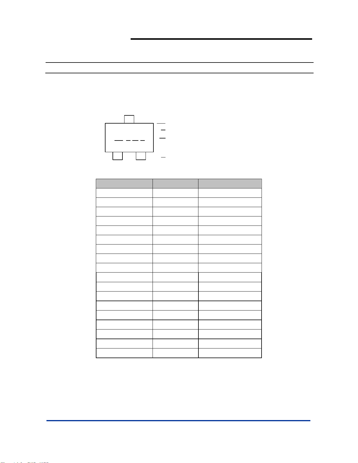
Marking Information
(1) SOT23 and SOT23R
( Top View )
AP7333
300mA, Low Quiescent Current, Fast Transient
Low Dropout Linear Regulator
XX
3
Y W
XX : Identification code
Y
: Year 0~9
W
X
: Week : A~Z : 1~26 week;
a~z : 27~52 week; z represents
52 and 53 week
X
1 2
: A~Z : Green
Device Package Identification Code
AP7333-10SA SOT23
AP7333-12SA SOT23
AP7333-15SA SOT23
AP7333-18SA SOT23
AP7333-20SA SOT23
AP7333-25SA SOT23
AP7333-28SA SOT23
AP7333-30SA SOT23
AP7333-33SA SOT23
AP7333-10SR SOT23R
AP7333-12SR
AP7333-15SR
AP7333-18SR
AP7333-20SR
AP7333-25SR
AP7333-28SR
AP7333-30SR
AP7333-33SR
SOT23R RB
SOT23R RC
SOT23R RD
SOT23R RE
SOT23R RF
SOT23R RG
SOT23R RH
SOT23R RJ
JR
JS
JT
JU
JV
JW
JX
JY
JZ
RA
AP7333 Rev. 2 10 of 12 NOVEMBER 2009
www.diodes.com © Diodes Incorporated
Page 11
300mA, Low Quiescent Current, Fast Transient
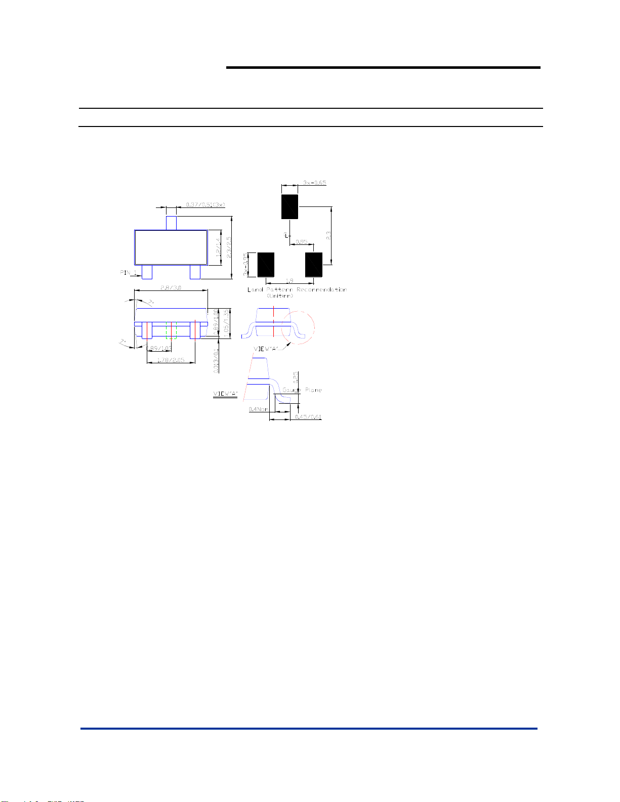
Package Information (All Dimensions in mm)
(1) Package Type: SOT23 and SOT23R
AP7333
Low Dropout Linear Regulator
AP7333 Rev. 2 11 of 12 NOVEMBER 2009
www.diodes.com © Diodes Incorporated
Page 12

AP7333
300mA, Low Quiescent Current, Fast Transient
Low Dropout Linear Regulator
IMPORTANT NOTICE
DIODES INCORPORATED MAKES NO WARRANTY OF ANY KIND, EXPRESS OR IMPLIED, WITH REGARDS TO THIS
DOCUMENT, INCLUDING, BU T NOT LIMI TED TO, T HE IMPLIE D WARRANT IES OF ME RCHANTABILIT Y AND FI TNESS FOR A
PARTICULAR PURPOSE (AND THEIR EQUIVALENTS UNDER THE LAWS OF ANY JURISDICTION).
Diodes Incorporated and its subsidiaries reserve the right to make modifications, enhancements, improvements, corrections or other
changes without further notice to this document and any product described herein. Diodes Incorporated does not assume any
liability arisi ng out of the application or use of this document or any product descr ibed herein; neither does Diode s Incorporated
convey any license under its patent or trademark rig hts, nor the rights of othe rs. Any Customer or user of this docume nt or products
described herein in such applications shall assume all risks of such use and will agree to hold Diodes Incorporated and all the
companies whose products are represented on Diodes Incorporated website, harmless against all damages.
Diodes Incorporat ed does not warrant or accept a ny liabil ity whatsoeve r in respect of any p roducts purc hase d through unau thori zed
sales channel.
Should Customers purch ase or use Diodes Incorpo rated products for an y unintended or unau thorized applic ation, Customers sh all
indemnify and hold Dio des Inc orporated and its re presen tatives harmle ss against all cla ims, d amages, expens es, a nd attor ney fees
arising out of, directly or indirectly, any claim of personal injury or death associated with such unintended or unauthorized
application.
Products described here in may be covered by one or more Unit ed States, i nternationa l or foreign patents p ending. Product n ames
and markings noted herein may also be covered by one or more United States, i nte rn ational or foreign trademarks.
LIFE SUPPORT
Diodes Incorporated products are specifically not authorized for use as critical components in life support devices or systems
without the express written approval of the Chief Executi ve Off icer of Diodes Incorporate d. As us e d herei n:
A. Life support devices or systems are devices or systems which:
1. are intended to implant into the body, or
2. support or sustain life and whose failure to perform when properly used in accordance with instructions for use provided
in the labeling can be reasonably expected to result in significant injury to the user.
B. A crit ical com ponent is any c omponent in a life sup port devic e or system whose failure to perform c an be reasona bly expec ted
to cause the failure of the life support device or to affect its safety or effectiveness.
Customers repres ent that th ey have all necessar y expertis e in th e safety a nd regul ator y ramific ations of t heir lif e support devic es or
systems, and acknowledge and agree that they are solely responsible for all legal, regulatory and safety-related requirements
concerning their products and any use of Diodes Incorporated products in such safety-critical, life support devices or systems,
notwithstandin g any devices- or systems-related i nformation or support that may be provided by Diodes Incorporated. Further,
Customers must full y indemnify Diode s Incorporat ed and its represent atives ag ainst any damages ari sing out of th e use of Diodes
Incorporated products in such safety-critical, life support devices or systems.
Copyright © 2009, Diodes Incorporated
www.diodes.com
AP7333 Rev. 2 12 of 12 NOVEMBER 2009
www.diodes.com © Diodes Incorporated
 Loading...