

Page 1
NEW PRODUCT
F
F
C
C
Y
500 kHz 18V 3A SYNCHRONOUS DC/DC BUCK CONVERTER
Description
The AP6507 is a 500kHz switching frequency internal
compensated synchronous DCDC buck converter. It has
integrated compensation, and low R
high and low side
DSON
MOSFETs.
The AP6507 enables continues load current of up to 3A with
efficiency as high as 93%.
The AP6507 features current mode control operation, which
enables fast transient response times and easy loop
stabilization.
The AP6507 simplifies board layout and reduces space
requirements with its high level of integration and minimal
need for external components, making it ideal for distributed
power architectures.
The AP6507 is available in a standard Green SO-8EP
package with exposed PAD for improved thermal
performance and is RoHS compliant.
Features
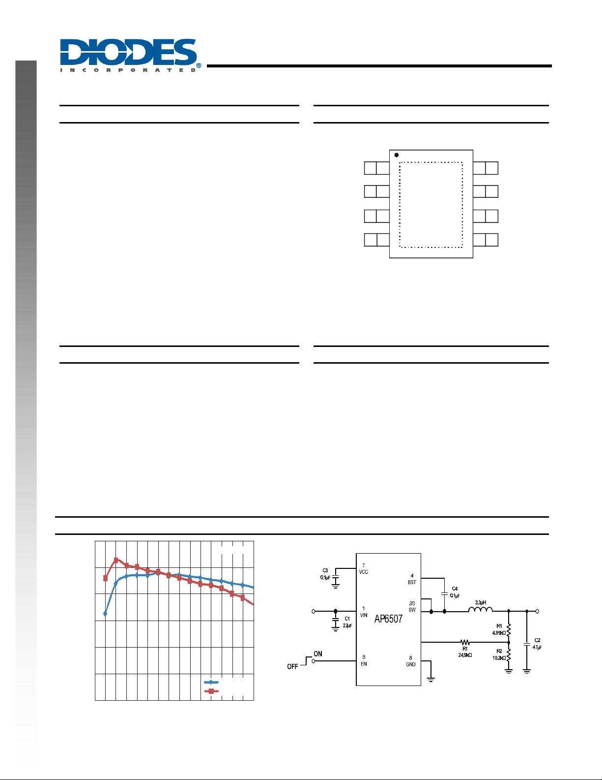
Pin Assignments
1
IN
SW
BST
2
3
4
Applications
(Top View)
SO-8EP
AP6507
8
GND
V
7
CC
6
FBSW
5
EN
• VIN 4.5V to 18V
• V
adjustable to 0.8V
OUT
• 500kHz switching frequency
• Enable pin
• Protection:
o OCP
o Thermal Shutdown
• Lead Free Finish/ RoHS Compliant (Note 1)
Note: 1. EU Directive 2002/95/EC (RoHS). All applicable RoHS exemptions applied. Please visit our website at
http://www.diodes.com/products/lead_free.html
.
• Gaming Consoles
• TV sets and Monitors
• Set Top Boxes
• Distributed power systems
• Home Audio
• Consumer electronics
Typical Application Circuit
100
90
80
(%)
70
IEN
I
60
E
V = 2.5V
OUT
50
40
0
1
LOAD CURRENT (A)
Efficiency vs. Load Current
AP6507
Document number: DS33435 Rev. 3 - 2
V = 12V
IN
V = 5V
IN
2
3
www.diodes.com
1 of 13
October 2011
© Diodes Incorporated
Page 2
Pin Descriptions
Pin # Name Description
1 IN
2, 3 SW Switch Output. Use wide PCB trace to make the connection.
4 BST
5 EN
6 FB
7
8
NEW PRODUCT
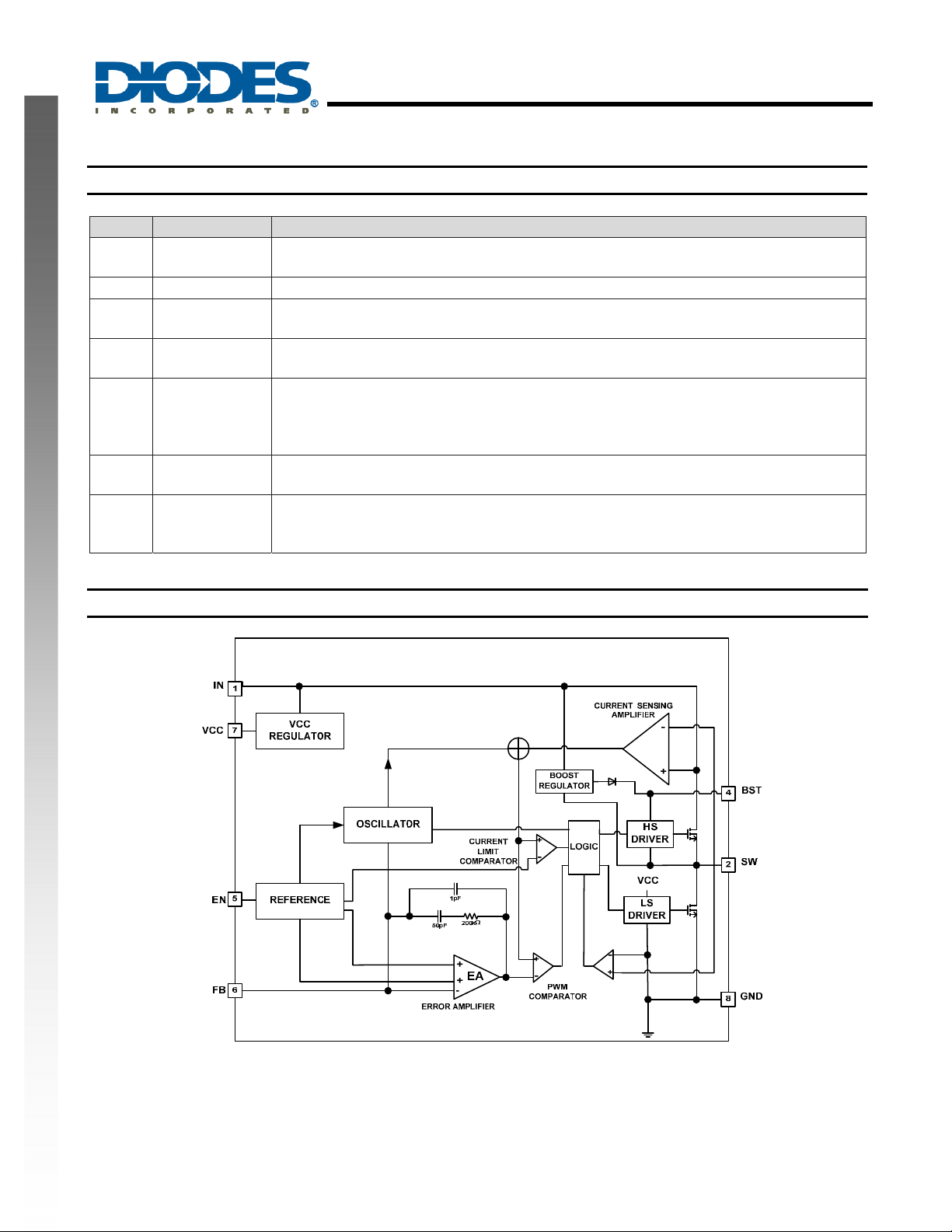
Functional Block Diagram
V
CC
GND
Exposed PAD
AP6507
500 kHz 18V 3A SYNCHRONOUS DC/DC BUCK CONVERTER
Supply Voltage. The AP6507 operates from a 4.5V to 18V input rail. C1 is needed to
decouple the input rail. Use wide PCB trace to make the connection.
Bootstrap. A capacitor connected between SW and BS pins is required to form a floating
supply across the high-side switch driver.
EN=1 to enable the chip. For automatic start-up, connect EN pin to VIN by proper EN resistor
divider as Figure 1 shows.
Feedback. An external resistor divider from the output to GND, tapped to the FB pin, sets the
output voltage. To prevent current limit run away during a short circuit fault condition the
frequency fold-back comparator lowers the oscillator frequency when the FB voltage is below
500mV.
BIAS Supply. Decouple with 0.1μF – 0.22μF cap. The capacitance should be no more than
0.22μF
System Ground. This pin is the reference ground for the regulated output voltage. For this
reason care must be taken in its PCB layout. Suggested to be connected to GND with copper
and vias.
AP6507
Document number: DS33435 Rev. 3 - 2
2 of 13
www.diodes.com
October 2011
© Diodes Incorporated
Page 3
AP6507
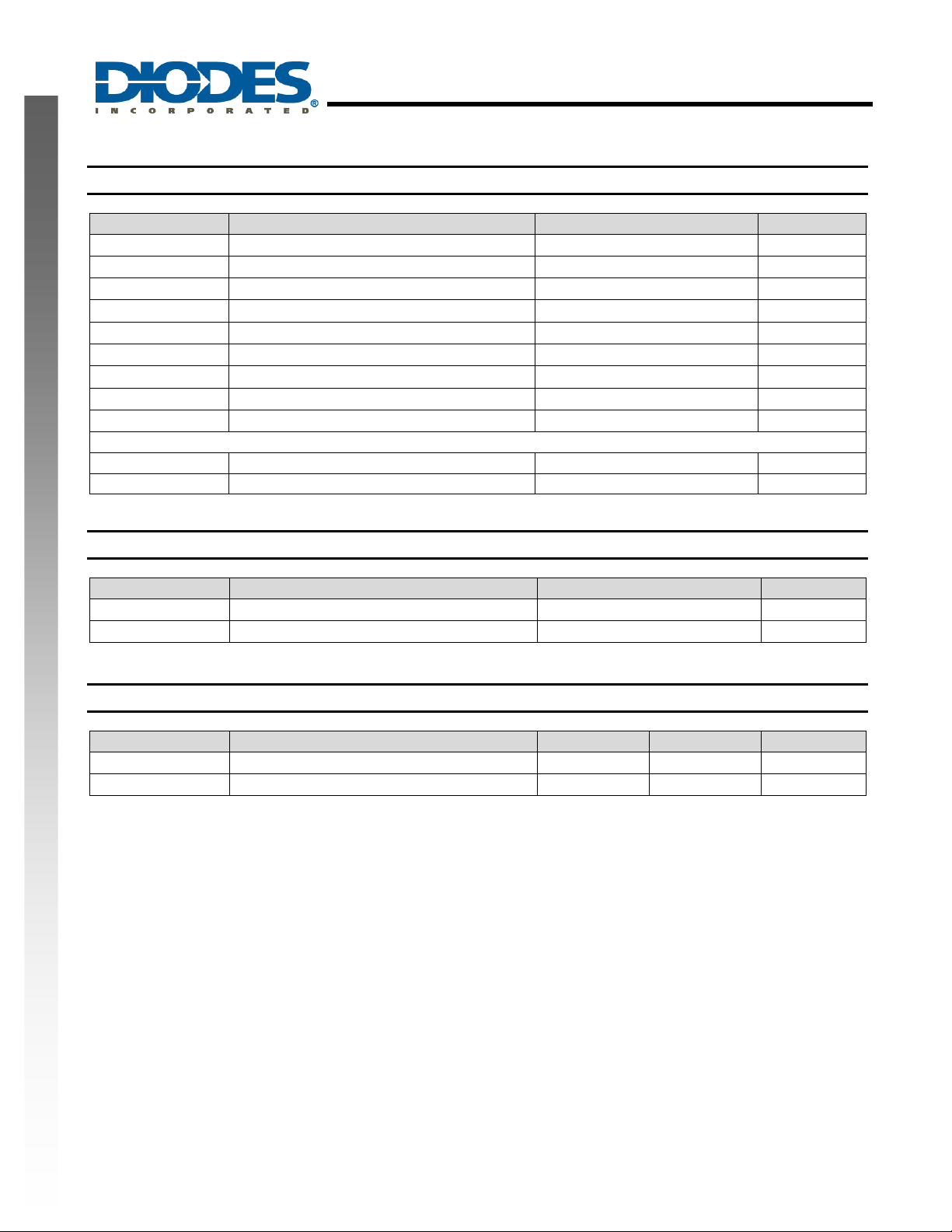
Absolute Maximum Ratings (T
Symbol Parameter Rating Unit
VIN
VSW
VBS
VFB
VEN
V
COMP
TST
TJ
TL
ESD Susceptibility (Note 3)
HBM Human Body Model 3 kV
MM Machine Model 300 V
NEW PRODUCT
Thermal Resistance (Note 4)
Symbol Parameter Rating Unit
θ
JA
θ
JC
Recommended Operating Conditions (Note 5)
Symbol Parameter Min Max Unit
VIN
TA
Notes: 2. Stresses greater than the 'Absolute Maximum Ratings' specified above, may cause permanent damage to the device. These are stress ratings
only; functional operation of the device at these or any other conditions exceeding those indicated in this specification is not implied. Device
reliability may be affected by exposure to absolute maximum rating conditions for extended periods of time.
3. Semiconductor devices are ESD sensitive and may be damaged by exposure to ESD events. Suitable ESD precautions should be taken when
handling and transporting these device.
4. Test condition for SO-8EP: Device mounted on 2"*2" FR-4 substrate PC board, 2oz copper, with minimum recommended pad on top layer and
thermal vias to bottom layer ground plane.
5. The device function is not guaranteed outside of the recommended operating conditions.
Supply Voltage
Switch Node Voltage -0.3 to 20 V
Bootstrap Voltage
Feedback Voltage –0.3 to +6 V
Enable/UVLO Voltage –0.3 to +6 V
Comp Voltage –0.3 to +6 V
Storage Temperature -65 to +150 °C
Junction Temperature +150 °C
Lead Temperature +260 °C
Junction to Ambient 56 °C/W
Junction to Case 16 °C/W
Supply Voltage
Operating Ambient Temperature Range
500 kHz 18V 3A SYNCHRONOUS DC/DC BUCK CONVERTER
= 25°C)
A
19
VSW + 6
4.5
-40
18 V
+85 °C
V
V
AP6507
Document number: DS33435 Rev. 3 - 2
3 of 13
www.diodes.com
October 2011
© Diodes Incorporated
Page 4
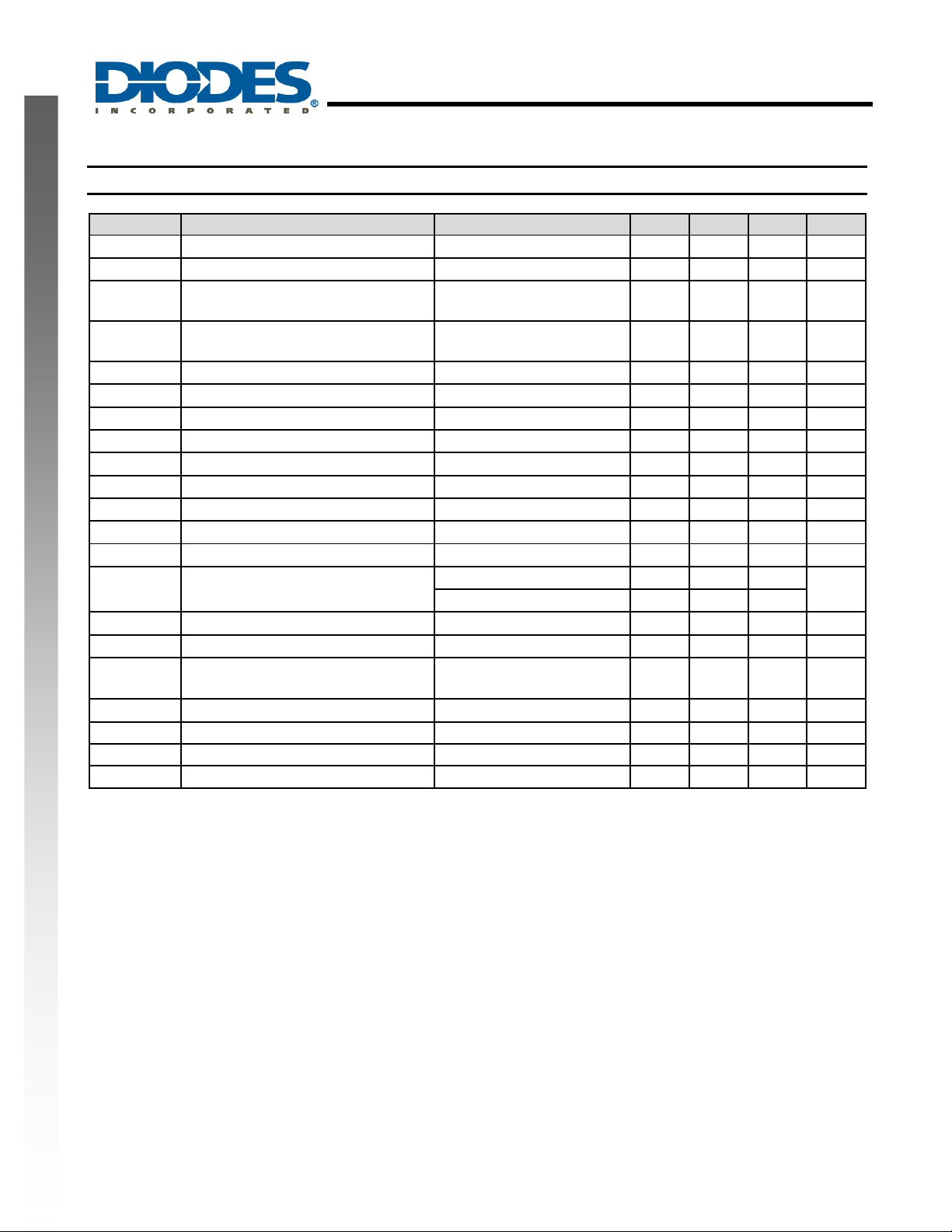
Electrical Characteristics (V
Symbol Parameter Test Conditions Min Typ. Max Unit
IIN
IIN
R
DS(ON)1
R
DS(ON)2
SW
LKG
I
Limit
FSW
FFB
D
MAX
VFB
IFB
V
NEW PRODUCT
EN_Rising
V
EN_HYS
IEN
EN
TD-Off
INUV
INUV
HYS
VCC
VCC Load Regulation Icc=5mA 5 %
Soft-Start Period 2 ms
TSD
Note: 6. Guaranteed by design
AP6507
Document number: DS33435 Rev. 3 - 2
Shutdown Supply Current
Supply Current (Quiescent)
High-Side Switch On-Resistance
(Note 6)
Low-Side Switch On-Resistance
(Note 6)
Switch Leakage Current
Current Limit 5.8 A
Oscillator Frequency
Fold-back Frequency
Maximum Duty Cycle
Feedback Voltage
Feedback Current
EN Rising Threshold 1.1 1.3 1.5 V
EN Threshold Hysteresis 0.4 V
EN Input Current
EN Turn Off Delay (Note 6) 5 μs
V
Vth
Under Voltage Threshold Rising
IN
V
Under Voltage Threshold
IN
Hysteresis
VCC Regulator 5 V
Thermal Shutdown 140 °C
AP6507
500 kHz 18V 3A SYNCHRONOUS DC/DC BUCK CONVERTER
= 12V, TA = +25°C, unless otherwise noted)
IN
VEN = 0V
VEN = 2.0V, VFB = 1.0V
120 mΩ
20 mΩ
V
= 0V, VSW = 0V
EN
V
= 0.75V
FB
V
= 300mV
FB
VFB = 700mV
TA = -40°C to +85°C
V
= 800mV
FB
V
= 2V
EN
VEN = 0V
4.0 4.2 4.4 V
200 mV
4 of 13
www.diodes.com
15 µA
1.2 mA
0 10 µA
350 500 650 kHz
0.3
80 85 %
788 808 828 mV
10 50 nA
2
0
© Diodes Incorporated
fSW
μA
October 2011
Page 5
O
Y C
R
R
C
CUR
RENT
T
O
P
O
A
G
OUT
PUT VOLTAG
E
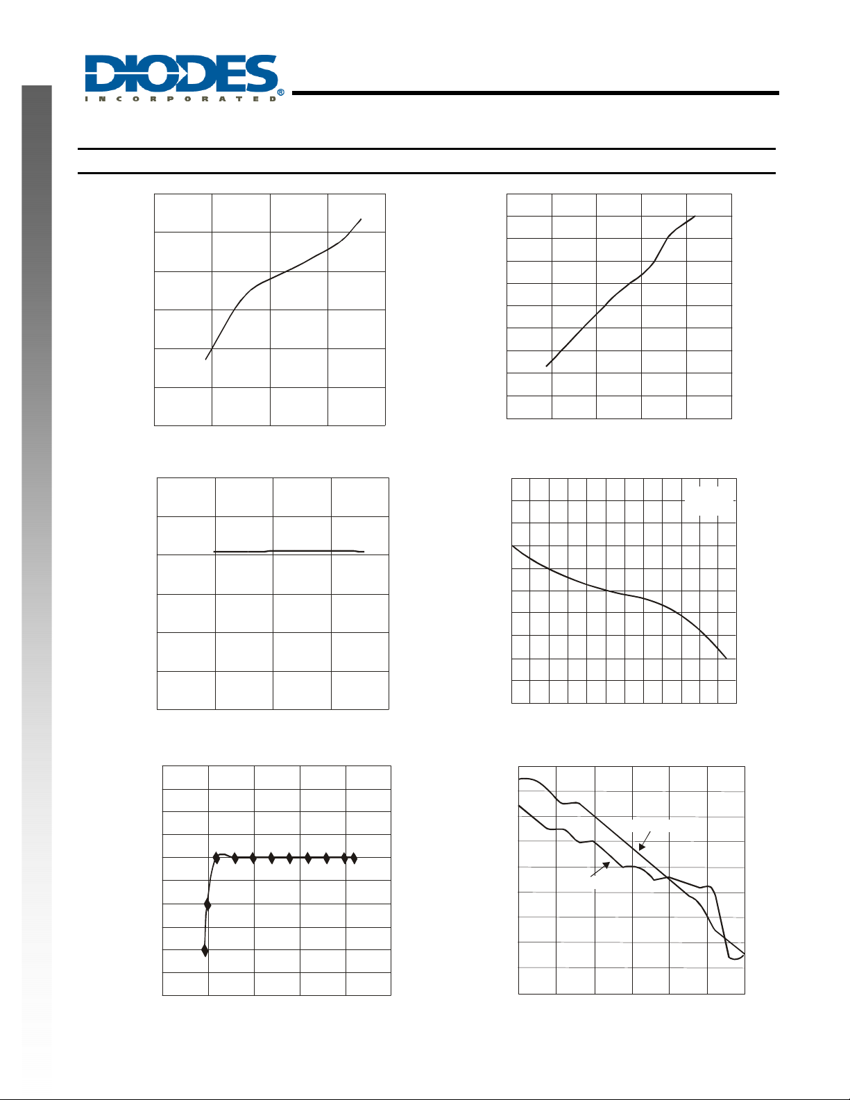
Typical Performance Graphs (V
NEW PRODUCT
1.3
1.25
1.2
1.15
1.1
1.05
QUIESCENT SUPPLY CURRENT (mA)
1
0 5 10 15 20
Quiescent Supply Current vs. Input Voltage
5.05
5.045
INPUT VOLTAGE (V)
AP6507
500 kHz 18V 3A SYNCHRONOUS DC/DC BUCK CONVERTER
= 12V, V
IN
= 1.2V, TA = +25°C, unless otherwise noted
OUT
20
18
16
ENT (µA)
14
U
12
10
8
6
WN SUPPL
4
2
SHUTD
0
0 5 10 15 25
Shutdown Supply Current vs. Input Voltage
INPUT VOLTAGE ( V)
7
6.8
6.6
20
V = 12V
IN
V = 1.2V
OUT
6.4
5.04
5.035
CC
V (V)
5.03
5.025
5.02
0 5 10 15 20
1.225
1.2245
1.224
1.2235
E (V)
1.223
LT
1.2225
UT V
1.222
UT
1.2215
1.221
1.2205
1.22
0 5 10 15 20 25
INPUT VOLTAGE (V)
V Regulator Line Regulation
C
INPUT VOLTAGE (V)
Line Regulation vs. Output Current
(A)
LIMI
(V)
6.2
6
5.8
5.6
5.4
5.2
5
-40
1.21
1.208
1.206
1.204
1.202
1.2
1.198
1.196
1.194
1.192
-10-2002010 30 5040 60 8070 90
TEMPERATURE (°C)
Current Li m it vs. Temperature
V = 12V
IN
V = 5V
IN
11.500.5 2.532
OUTPUT CURRENT (A)
Load Re gu lation vs. Output C ur r ent
AP6507
Document number: DS33435 Rev. 3 - 2
5 of 13
www.diodes.com
October 2011
© Diodes Incorporated
Page 6
F
FICIENCY
F
FIC
C
Y
F
FIC
C
Y
F
FIC
C
Y
500 kHz 18V 3A SYNCHRONOUS DC/DC BUCK CONVERTER
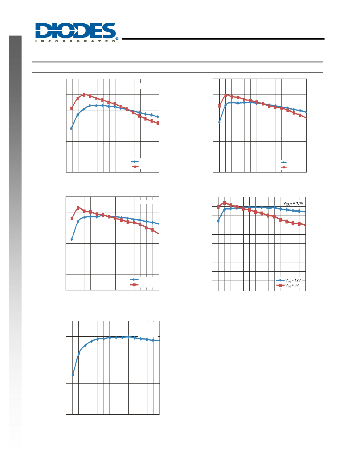
Typical Performance Graphs (cont.) (V
100
90
V = 1.2V
OUT
= 12V, V
IN
AP6507
= 1.2V, TA = +25°C, unless otherwise noted
OUT
100
V = 1.8V
OUT
90
NEW PRODUCT
80
(%)
70
60
E
50
40
100
90
80
(%)
70
IEN
60
E
50
40
80
(%)
70
IEN
60
E
100
90
50
40
V = 12V
IN
V = 5V
IN
0
1
2
3
LOAD CURRENT (A)
Efficiency vs. Load Current
V = 12V
IN
V = 5V
IN
0
1
2
3
LOAD CURRENT (A)
Efficiency vs. Load Current
V = 2.5V
OUT
80
70
60
50
40
EFFICIENCY (%)
30
20
V = 12V
IN
V = 5V
IN
0
1
2
3
LOAD CURRENT (A)
Efficiency vs. Load Current
10
0
0
1
2
3
LOAD CURRENT (A)
Efficiency vs. Load Current
100
90
80
(%)
70
IEN
60
E
50
40
0
1
LOAD CURRENT (A)
Efficiency vs. Load Current
AP6507
Document number: DS33435 Rev. 3 - 2
2
V = 12V
IN
V = 5V
OUT
L = 3.3µH
3
6 of 13
www.diodes.com
October 2011
© Diodes Incorporated
Page 7

500 kHz 18V 3A SYNCHRONOUS DC/DC BUCK CONVERTER
Typical Performance Characteristics
AP6507
NEW PRODUCT
VIN = 12V, V
= 1.2V, L = 3.3µH, C1 = 22µF, C2 = 47µF, TA = +25°C, unless otherwise noted
OUT
Time- 2µs/div
Steady State Test
=3A
I
OUT
Load Transient Test
=1.5A to 3A. Step at 0.8A/µs
I
OUT
Time- 500us/div
Start-up Through Enable (No Load)
Start-up through V
Time- 200µs/div
Time- 2ms/div
(No load)
IN
Time- 50µs/div
Shutdown Through Enable (No Load)
Time- 50µs/div
Short Circuit Entry
AP6507
Document number: DS33435 Rev. 3 - 2
Time- 50µs/div
7 of 13
www.diodes.com
Shutdown Through Enable (I
Time- 100µs/div
Short Circuit Recovery
=1A)
OUT
October 2011
© Diodes Incorporated
Page 8

500 kHz 18V 3A SYNCHRONOUS DC/DC BUCK CONVERTER
Typical Performance Characteristics
AP6507
VIN = 12V, V
NEW PRODUCT
AP6507
Document number: DS33435 Rev. 3 - 2
OUT
= 1.2V, L = 3.3µH, C1 = 22µF, C2 = 47µF, TA = +25°C, unless otherwise noted
Time- 1µs/div
Input Voltage Ripple
Time- 2µs/div
Output Voltage Ripple
8 of 13
www.diodes.com
October 2011
© Diodes Incorporated
Page 9
500 kHz 18V 3A SYNCHRONOUS DC/DC BUCK CONVERTER
Application Information
Theory of Operation
The AP6507 is a 3A current mode, synchronous buck
regulator with built in power MOSFETs. Current mode
control assures excellent line and load regulation and a
wide loop bandwidth for fast response to load transients.
Figure 4 depicts the functional block diagram of AP6507 is
given on page 2.
The operation of one switching cycle can be explained as
follows. At the beginning of each cycle, HS (high-side)
MOSFET is off. The EA (error amplifier) output voltage is
higher than the current sensing amplifier output, and the
current comparator’s output is low. The rising edge of the
500kHz oscillator clock signal sets the RS Flip-Flop. Its
output turns on HS MOSFET. The current sensing
amplifier is reset for every switching cycle.
When the HS MOSFET is on, inductor current starts to
increase. The current sensing amplifier senses and
amplifies the inductor current. Since the current mode
control is subject to sub-harmonic oscillations that peak at
NEW PRODUCT
half the switching frequency, slope compensation is
utilized. This will help to stabilize the power supply. This
slope compensation is summed to the current sensing
amplifier output and compared to the error amplifier output
by the PWM comparator. When the sum of the current
sensing amplifier output and the slope compensation
signal exceeds the EA output voltage, the RS Flip-Flop is
reset and HS MOSFET is turned off.
For one whole cycle, if the sum of the current sensing
amplifier output and the slope compensation signal does
not exceed the EA output, then the falling edge of the
oscillator clock resets the flip-flop. The output of the EA
increases when feedback voltage (VFB) is lower than the
reference voltage of 0.808V. This also increases the
inductor current as it is proportional to the EA voltage.
When the HS MOSFET turns off, the synchronous LS
MOSFET turns on until the next clock cycle begins. There
is a “dead time” between the HS turn off and LS turn on
that prevents the switches from “shooting through” from
the input supply to ground.
The voltage loop is internally compensated with the 50pF
and 200kΩ RC network. The maximum EA voltage output
is precisely clamped at 2.1V.
Internal Regulator
Most of the internal circuitry including the low-side driver is
powered from the 5V internal regulator. When Vin is less
than 5V, this internal regulator cannot maintain the 5V
regulation and hence the output voltage would also drop
from regulation.
AP6507
Enable
The enable (EN) input allows the user to control turning
on or off the converter. To enable the converter EN must
be pulled above the ‘EN Rising Threshold’ and to dis able
the converter EN must be pulled below ‘EN falling
Threshold’ (EN rising threshold – En threshold
Hysteresis).
Few conditions on EN function:
1) EN must be pulled low for at least 5us to disable the
regulator.
2) The voltage on EN cannot exceed 5V.
3) The AP6507 can be enabled by Vin through a voltage
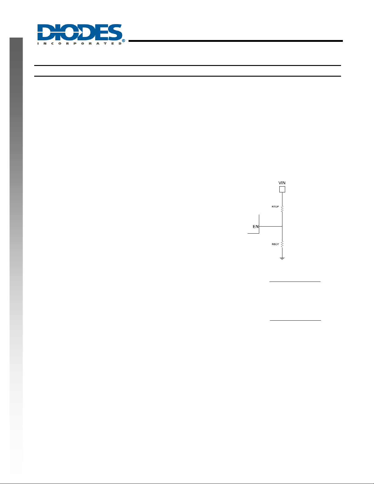
divider as shown in the figure 3 below.
Figure 1. EN Divider Network
VV
=
−−
RISEENRISEIN
Where
VV
=
−−
Where
RISEENV−
FALLENFALLIN
FALLENV−
= 1.3V(TYP)
Internal Soft Start
Soft start is traditionally implemented to prevent an
excess inrush current. This in turn prevents the
converter output voltage from overshooting when it
reaches regulation. The AP6507 has an internal current
source with a soft start capacitor to ramp the reference
voltage from 0V to 0.808V. The soft start time is i ntern ally
fixed at 2ms (TYP). The soft start sequence is reset when
there is a thermal shutdown, Under Voltage Lockout
(UVLO) or when the part is disabled using the EN pin.
+
BOTTOP
1MΩ||R
BOT
+
BOTTOP
1MΩ||R
BOT
= 0.9V(TYP)
1MΩ||R(R
1MΩ||R(R
AP6507
Document number: DS33435 Rev. 3 - 2
9 of 13
www.diodes.com
October 2011
© Diodes Incorporated
Page 10
500 kHz 18V 3A SYNCHRONOUS DC/DC BUCK CONVERTER
Application Information (cont.)
AP6507
Current Limit Protection
In order to reduce the total power dissipation and to
protect the application, AP6507 has cycle-by-cycle current
limiting implementation. The voltage drop across the
internal high-side MOSFET is sensed and compared with
the internally set current limit threshold. This voltage dro p
is sensed at about 30ns after the HS turns on. This voltage
drop is proportional to the peak inductor current. When the
peak inductor current exceeds the set current limit
threshold, current limit protection is activated. During th is
time the feedback voltage (VFB) drops down. When the
voltage at the FB pin reaches 0.3V, the interna l oscillator
shifts the frequency from the normal operating fr equency
of 500kHz to a fold-back frequency of 1 50kH z. The current
limit is reduced to 70% of nominal current limit when the
part is operating at 150kHz. This low fold-back frequenc y
prevents current runaway.
Under Voltage Lockout (UVLO)
NEW PRODUCT
Under Voltage Lockout is implemented to preve nt the IC
from operating under insufficient input voltages. The
AP6507 has a UVLO comparator that monitors the input
voltage and the internal bandgap reference. If the input
voltage falls below 4.0V, the AP6507 will latch an under
voltage fault. In this event the AP6507 will be disabled and
power has to be re-cycled to reset the UVLO fault.
Thermal Shutdown
The AP6507 has on-chip thermal protection that prevents
damage to the IC when the die temperature exceeds safe
margins. It implements a thermal sensing to monitor the
operating junction temperature of the IC. Once the die
temperature rises to approximately 140°C, the thermal
protection feature gets activated. The internal thermal
sense circuitry turns the IC off thus preventing the po wer
switch from damage.
A hysteresis in the thermal sense circuit allows the device
to cool down to approximately 120°C before the IC is
enabled again through soft start. This thermal hysteresis
feature prevents undesirable oscillations of the thermal
protection circuit.
Setting the Output Voltage
The output voltage can be adjusted from 0.808V to 15V
using an external resistor divider.
resistor selection for common output voltages. Resistor
R1 is selected based on a design tradeoff between
efficiency and output voltage accuracy. F or high values of
R1 there is less current consumption in the feedback
network. However the trade off is output voltage accuracy
Table 1 shows a list of
due to the bias current in the error amplifier. R2 can b e
−⋅= 1
⎞
⎟
⎟
⎠
determined by the following equation:
V
⎛
OUT
⎜
RR
21
⎜
0.808
⎝
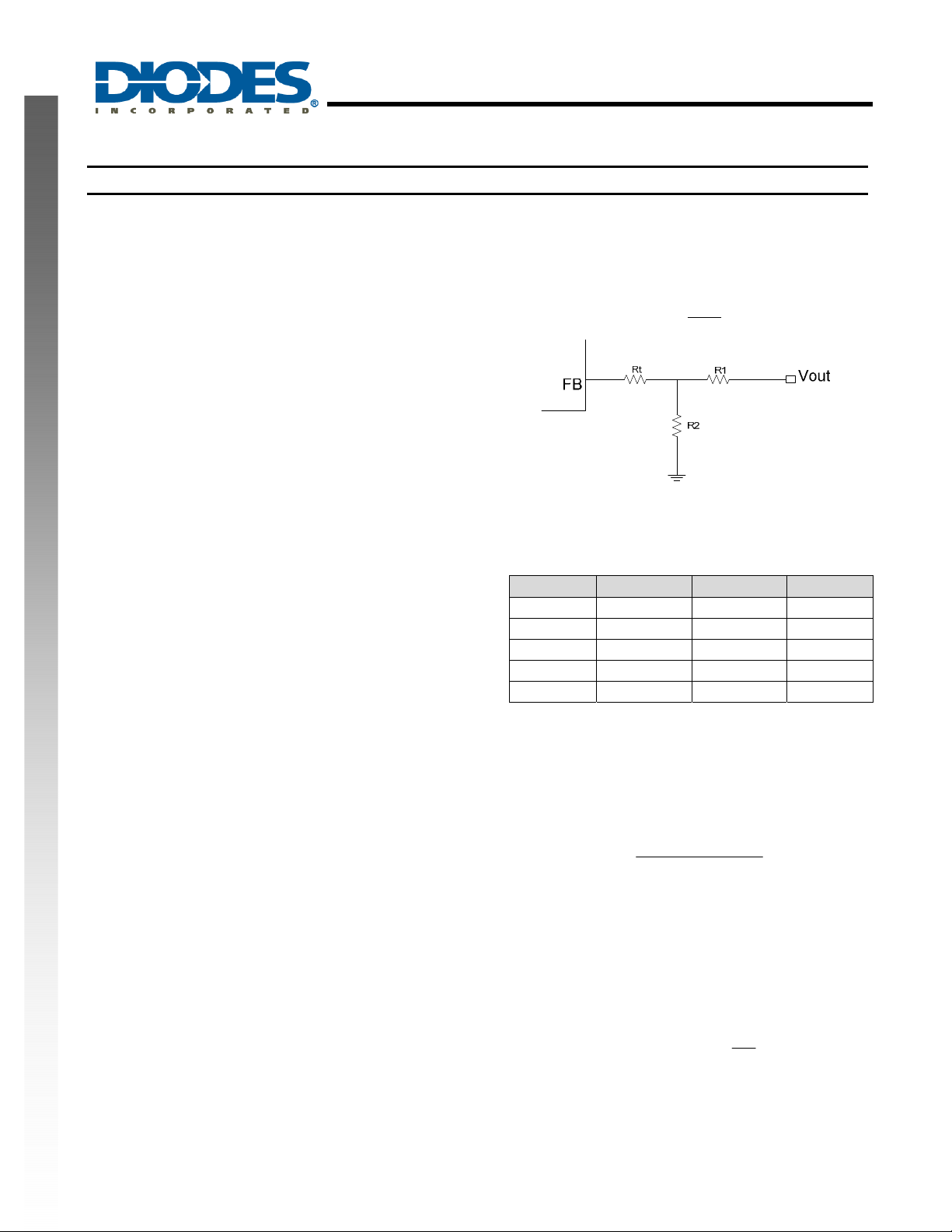
Figure 2. Feedback Divider Network
When output voltage is low, a T-type net work as shown
in Figure 2 is recommended.
V
(V) R1 (kΩ) R2 (kΩ) Rt (kΩ)
OUT
1.2 4.99 10.2 24.9
1.8 4.99 (1%) 4.02 (1%) 35.7
2.5 40.2 (1%) 19.1 (1%) 24.9
3.3 40.2 (1%) 13 (1%) 24.9
5 40.2 (1%) 7.68 (1%) 35.7
Table 1—Resistor Selection for Common Output
Voltages
Inductor
Calculating the inductor value is a critical factor in
designing a buck converter. For most designs, the
following equation can be used to calculat e the inductor
value;
=
L
ΔI
Where
And
Choose the inductor ripple current to be 30% of the
maximum load current. The maximum inductor peak
current is calculated from:
is the inductor ripple current.
L
f
is the buck converter switching frequency.
SW
−⋅
⋅⋅
II
LOADL(MAX)
)V(VV
OUTINOUT
fΔIV
SWLIN
ΔI
L
+=
2
AP6507
Document number: DS33435 Rev. 3 - 2
10 of 13
www.diodes.com
October 2011
© Diodes Incorporated
Page 11
500 kHz 18V 3A SYNCHRONOUS DC/DC BUCK CONVERTER
Application Information (cont.)
Inductor (cont.)
Peak current determines the required saturation current
rating, which influences the size of the inductor. Saturating
the inductor decreases the converter efficiency while
increasing the temperatures of the inductor and the
internal MOSFETs. Hence choosing an inductor with
appropriate saturation current rating is important .
A 1µH to 10µH inductor with a DC current rating of at least
25% percent higher than the maximum load current is
recommended for most applications. For highest
efficiency, the inductor’s DC resistance should be less
than 200mΩ. Use a larger inductance for improved
efficiency under light load conditions.
Input Capacitor
The input capacitor reduces the surge current drawn from
the input supply and the switching noise fr om the device.
The input capacitor has to sustain the ripple current
NEW PRODUCT
produced during the on time on the upper MOSFET. It
must hence have a low ESR to minimize the losses.
The RMS current rating of the input capacitor is a critical
parameter that must be higher than the RMS inp ut current.
As a rule of thumb, select an input capacitor which has an
RMS rating that is greater than half of the maximum load
current.
Due to large dI/dt through the input capacitors, electrol ytic
or ceramics should be used. If a tantalum must be used, it
must be surge protected. Otherwise, capacitor failure
could occur. For most applications, a 4.7µF ceramic
capacitor is sufficient.
Output Capacitor
The output capacitor keeps the output voltage ripple small,
ensures feedback loop stability and reduces the overshoot
of the output voltage. The output capacitor is a basic
component for the fast response of the power supply. In
fact, during load transient, for the first few microseconds it
supplies the current to the load. The converter recognizes
the load transient and sets the duty cycle to maximum, but
the current slope is limited by the inductor value.
Maximum capacitance required can be calculated from the
following equation:
Where
ΔV is the maximum output voltage overshoot.
ΔI
out
+
V V(Δ
out
inductor
)
L(I
C
=
o
2
)
2
2
−+
2
V
out
AP6507
ESR of the output capacitor dominates the output voltage
ripple. The amount of ripple can be calculated from the
equation below:
=
inductorcapacitor
An output capacitor with ample capacitance and l ow ESR
is the best option. For most applications, a 22µF ceramic
capacitor will be sufficient.
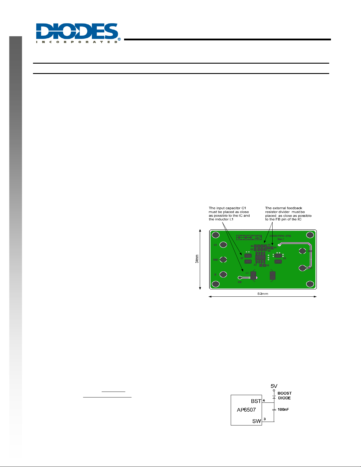
PC Board Layout
This is a high switching frequency converter. Hence
attention must be paid to the switching currents
interference in the layout. Switching current from one
power device to another can generate voltage transients
across the impedances of the interconnecting bond wires
and circuit traces. These interconnecting impedances
should be minimized by using wide, short printed circuit
traces.
AP6507 is exposed at the bottom of the package and
must be soldered directly to a well designed thermal pad
on the PCB. This will help to increase the power
dissipation.
External Bootstrap Diode
It is recommended that an external bootstrap diode be
added when the input voltage is lower than or equal to 5V
and the duty cycle is greater than 65%. This external
diode can be connected to the input or a 5V rail that is
available in the system. This helps improve the efficiency
of the converter. The bootstrap diode c an be a low cost
one such as BAT54 or a schottky that has a low Vf.
Figure 3. External Bootstrap Diode
ESR*ΔIVout
AP6507
Document number: DS33435 Rev. 3 - 2
11 of 13
www.diodes.com
October 2011
© Diodes Incorporated
Page 12
Ordering Information
AP6507
500 kHz 18V 3A SYNCHRONOUS DC/DC BUCK CONVERTER
AP6507 SP - 13
Package
SP : SO-8EP
Device
AP6507SP-13 SP SO-8EP 2500/Tape & Reel -13
Note: 7. Pad layout as shown on Diodes Inc. suggested pad layout document AP02001, which can be found on our website at
http://www.diodes.com/datasheets/ap02001.pdf.
Package
Code
Packaging
(Note 7)
Packing
13 : Tape & Reel
13” Tape and Reel
Quantity Part Number Suffix
Marking Information
NEW PRODUCT
( Top View )
5
: Year : 08, 09,10~
YY
WW
: Week : 01~52; 52
represents 52 and 53 week
E
X
: Internal Code
X
Logo
Part No
8
AP6507
WW X
YY
SO-8EP
G : Green
41
Package Outline Dimensions (All Dimensions in mm)
85
E1
14
b
9° (All si de s)
4° ± 3°
e
A1
D
A
N
7
°
F
Bottom View
E
45
°
E0
Exposed Pad
H
Q
C
Gauge Plane
Seating Plane
L
AP6507
Document number: DS33435 Rev. 3 - 2
12 of 13
www.diodes.com
SO-8EP (SOP-8L-EP)
Dim Min Max Typ
A 1.40 1.50 1.45
A1 0.00 0.13 -
b 0.30 0.50 0.40
C 0.15 0.25 0.20
D 4.85 4.95 4.90
E 3.80 3.90 3.85
E0 3.85 3.95 3.90
E1 5.90 6.10 6.00
e - - 1.27
F 2.75 3.35 3.05
H 2.11 2.71 2.41
L 0.62 0.82 0.72
N - - 0.35
Q 0.60 0.70 0.65
All Dimensions in mm
© Diodes Incorporated
October 2011
Page 13

NEW PRODUCT
AP6507
DIODES INCORPORATED MAKES NO WARRANTY OF ANY KIND, EXPRESS OR IMPLIED, WITH REGARDS TO THIS
DOCUMENT, INCLUDING, BUT NOT LIMITED TO, THE IMPLIED WARRANTIES OF MERCHANTABILITY AND FITNESS FOR A
PARTICULAR PURPOSE (AND THEIR EQUIVALENTS UNDER THE LAWS OF ANY JURISDICTION).
Diodes Incorporated and its subsidiaries reserve the right to make modifications, enhancements, improvements, corrections or other
changes without further notice to this document and any product described herein. Diodes Incorporated does not assume any liability
arising out of the application or use of this document or any product described herein; neither does Diodes Incorporated convey any
license under its patent or trademark rights, nor the rights of others. Any Customer or user of this document or produc ts described
herein in such applications shall assume all risks of such use and will agree to hold Diodes Incorporated and all the companies
whose products are represented on Diodes Incorporated website, harmless against all damages.
Diodes Incorporated does not warrant or accept any liability whatsoever in respec t of any products purchased t hrough unauthorized
sales channel.
Should Customers purchase or use Diodes Incorporated products for any unintended or unauthorized application, Customers shall
indemnify and hold Diodes Incorporated and its representatives harmless against all claims, damages, expenses, and attorney fees
arising out of, directly or indirectly, any claim of personal injury or death associated with such unintended or unauthorized application.
Products described herein may be covered by one or more United States, international or foreign patents pending. Product names
and markings noted herein may also be covered by one or more United States, international or foreign trademarks.
Diodes Incorporated products are specifically not authorized for use as critical components in life support devices or systems without
the express written approval of the Chief Executive Officer of Diodes Incorporated. As used herein:
A. Life support devices or systems are devices or systems which:
1. are intended to implant into the body, or
2. support or sustain life and whose failure to perform when properly used in accordance with instructions for use provided
in the labeling can be reasonably expected to result in significant injury to the user.
B. A critical component is any component in a life support device or system whose failure to perform can be reasonably expected
to cause the failure of the life support device or to affect its safety or effectiveness.
Customers represent that they have all necessary expertise in the safety and regulatory ramifications of their life support devices or
systems, and acknowledge and agree that they are solely responsible for all legal, regulatory and safety-related requirements
concerning their products and any use of Diodes Incorporated products in such safety-critical, life support devices or systems,
notwithstanding any devices- or systems-related information or support that may be provided by Diodes Incorporated. Further,
Customers must fully indemnify Diodes Incorporated and its representatives against any damages arising out of the use of Diodes
Incorporated products in such safety-critical, life support devices or systems.
Copyright © 2011, Diodes Incorporated
www.diodes.com
500 kHz 18V 3A SYNCHRONOUS DC/DC BUCK CONVERTER
IMPORTANT NOTICE
LIFE SUPPORT
AP6507
Document number: DS33435 Rev. 3 - 2
13 of 13
www.diodes.com
October 2011
© Diodes Incorporated
 Loading...