

Page 1
AP5725
WHITE LED STEP-UP CONVERTER
Description
The AP5725 is a step-up DC/DC converter specifically
designed to drive white LEDs with a constant current. The
device can drive 2 ~ 6 LEDs in series from a Li-Ion cell.
Series connection of the LEDs provides identical LED
currents resulting in uniform brightness and eliminates the
need for ballast resistors. For driving higher number of LEDs,
AP5725 also supports a single feedback of parallel
connected multiple strings of equal number of LEDs.
The AP5725 switches at 1.2MHz that allows the use of tiny
external components. A low 0.25V feedback voltage
minimizes power loss in the current setting resistor for better
efficiency.
Features
• High efficiency: 84% typical
• Fast 1.2MHz switching frequency
• Current limit and UVLO protections
• Internal thermal shutdown
• Internal Over Voltage Protection
• Integrated soft-start function
• SOT26, TSOT23-6 and DFN2020C-6: Available in
“Green” Molding Compound (No Br, Sb)
• Lead Free Finish/ RoHS Compliant (Note 1)
Notes: 1. EU Directive 2002/95/EC (RoHS). All applicable RoHS exemptions applied. Please visit our website at
http://www.diodes.com/products/lead_free.html.
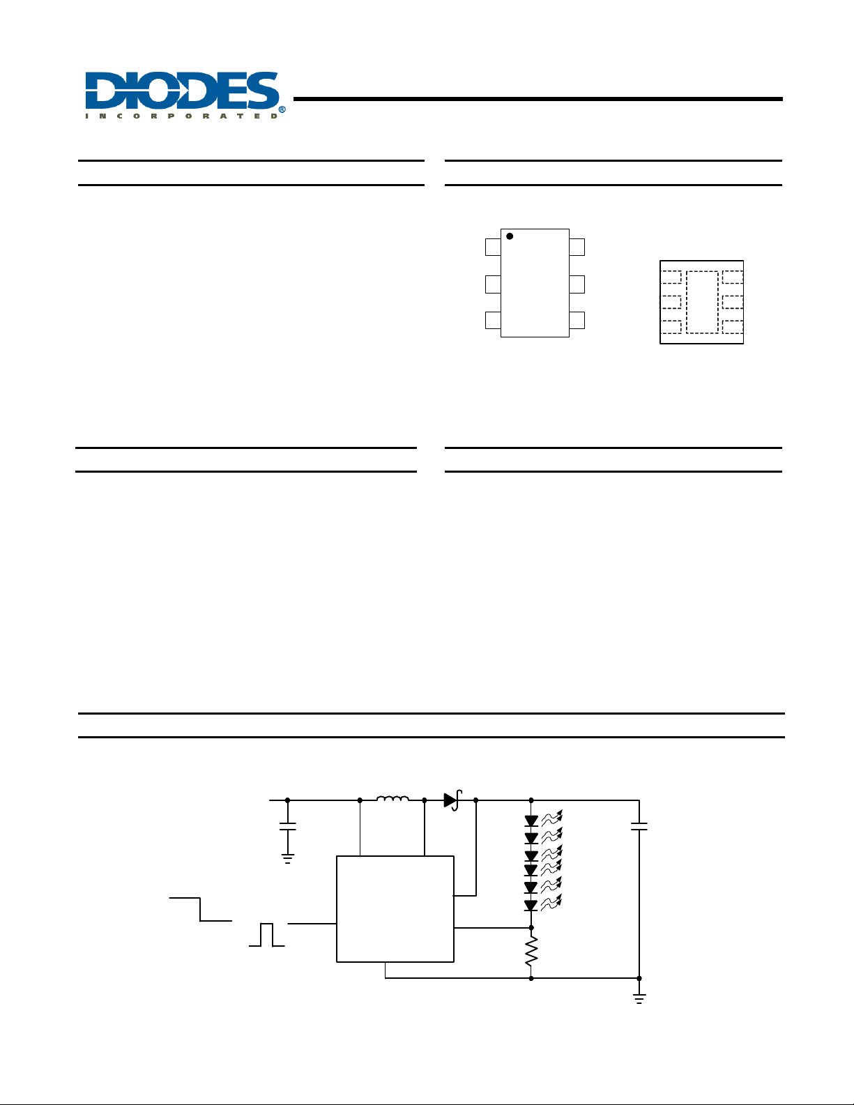
Pin Assignments
(Top View)
SW
GND
FB
1
2
3
VIN
6
5
OVP
7
4
EN
SOT26 / TSOT23-6
Applications
• Cellular Phones
• PDAs, Hand held Computers
• Digital Cameras
• MP3 Players
• GPS Receivers
SW
V
IN
OVP
DFN2020C-6
(Top View)
1
2
3
6
GND
5
FB
4
EN
Typical Application Circuit
V
IN
OFFON
PWM Dimming
AP5725
Document number: DS31844 Rev. 3 - 2
L1
22uH
C
IN
D1
1uF
V
AP5725
EN
IN
SW
OVP
FB
GND
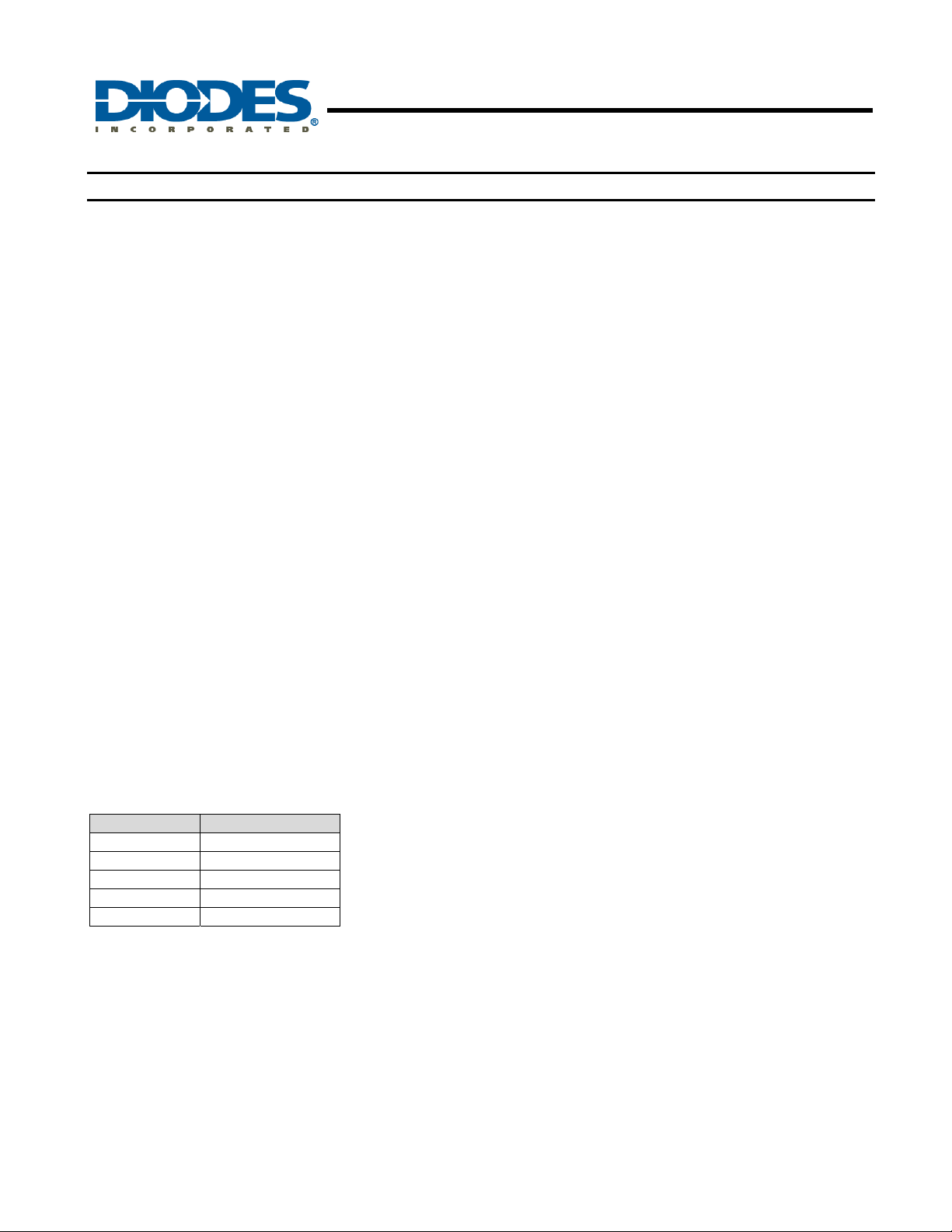
Figure 1. Typical Application Circuit
1 of 17
www.diodes.com
R
12
SET
2~6 LEDs
C
OUT
1uF
© Diodes Incorporated
July 2010
Page 2
WHITE LED STEP-UP CONVERTER
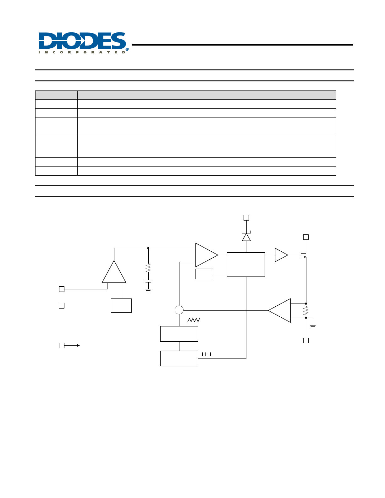
Pin Descriptions
Pin Name Description
SW Switch Pin. Connect inductor/diode here. Minimize trace area at this pin to reduce EMI.
GND GND pin.
FB
EN
OVP Output Voltage detect pin for over voltage protection.
VIN Input Supply Pin. Must be locally bypassed with 1μF or 2.2μF to reduce input noise.
Functional Block Diagram
Feedback Pin. Reference voltage is 0.25V. Connect cathode of lowest LED and a sense
resister here. Calculate resistor value according to the formula: R
= 0.25V / ILED
SET
Converter On/Off Control Input. A high input at EN turns the converter On, and a low input
turns it off. If On/Off control is not needed, connect EN to the input source for automatic
startup. The EN pin cannot be left floating.
OVP
5
AP5725
1
Comparator
-
A2
+
Rc
A1
-
+
FB
3
V
V
6
IN
REF
0.25V
Cc
Σ
OTP
CONTROL
LOGIC
Driver
+
SW
Q1
-
RAMP
Generator
EN
4
Enable
1.2MHz
Oscillator
2
GND
AP5725
Document number: DS31844 Rev. 3 - 2
2 of 17
www.diodes.com
July 2010
© Diodes Incorporated
Page 3
AP5725
WHITE LED STEP-UP CONVERTER
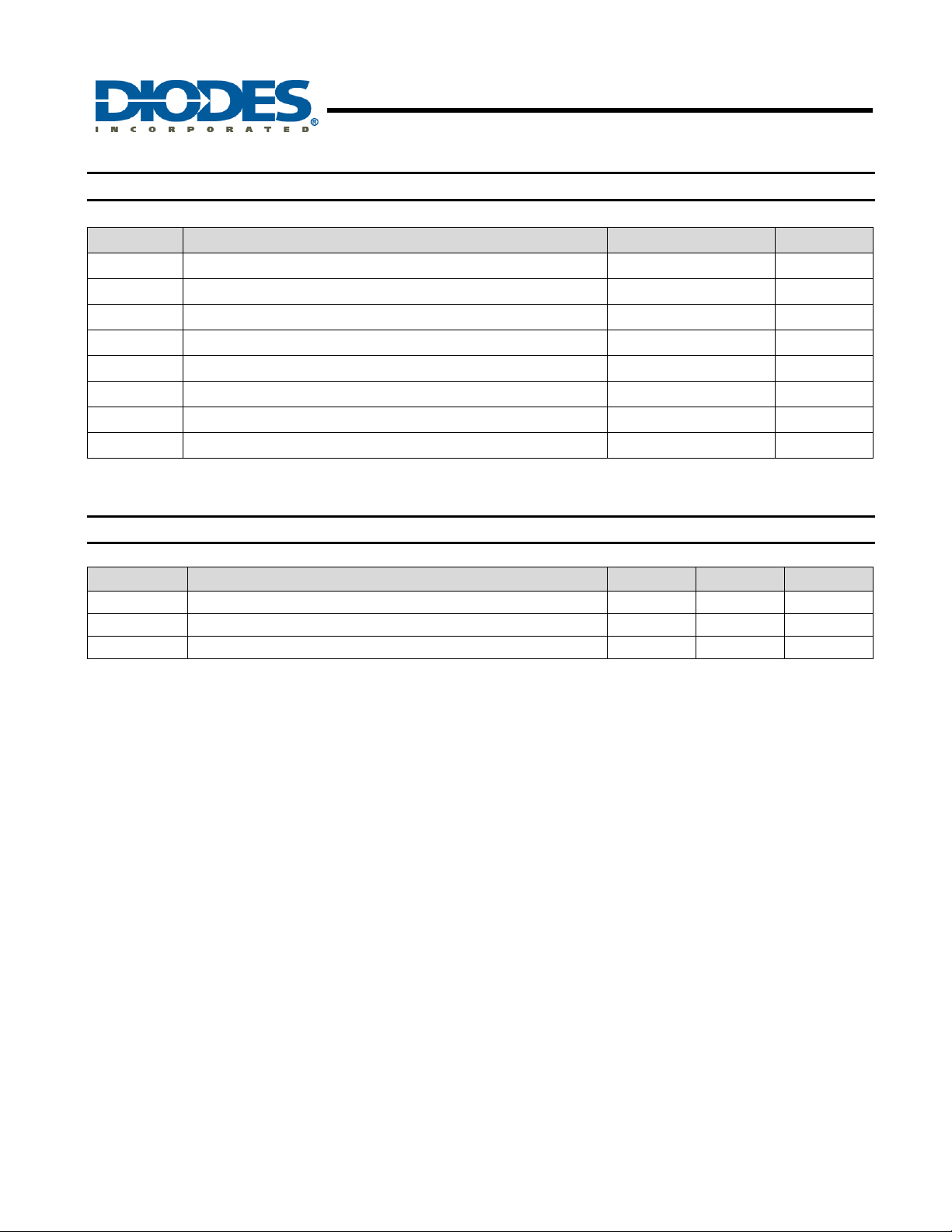
Absolute Maximum Ratings
Symbol Parameter Rating Unit
VIN VIN Pin Voltage -0.3~7 V
VSW SW Voltage -0.3~34 V
V
OVP Pin Voltage -0.3~35 V
OVP
VFB Feedback Pin Voltage -0.3~7 V
EN EN -0.3~7 V
T
Maximum Junction Temperature 150
J(MAX)
T
Lead Temperature 300
LEAD
T
Storage Temperature Range -65 to +150
ST
Caution: Operation above the absolute maximum ratings can cause device failure. These values, therefore, must not be exceeded under
any condition. Operation at the absolute maximum rating for extended periods, may reduce device reliability.
Recommended Operating Conditions
o
C
o
C
o
C
Symbol Parameter Min Max Unit
VIN Input Voltage 2.7 5.5 V
TJ Operating Junction Temperature -40 125
TA Operating Ambient Temperature -40 85
o
C
o
C
AP5725
Document number: DS31844 Rev. 3 - 2
3 of 17
www.diodes.com
July 2010
© Diodes Incorporated
Page 4
AP5725
WHITE LED STEP-UP CONVERTER
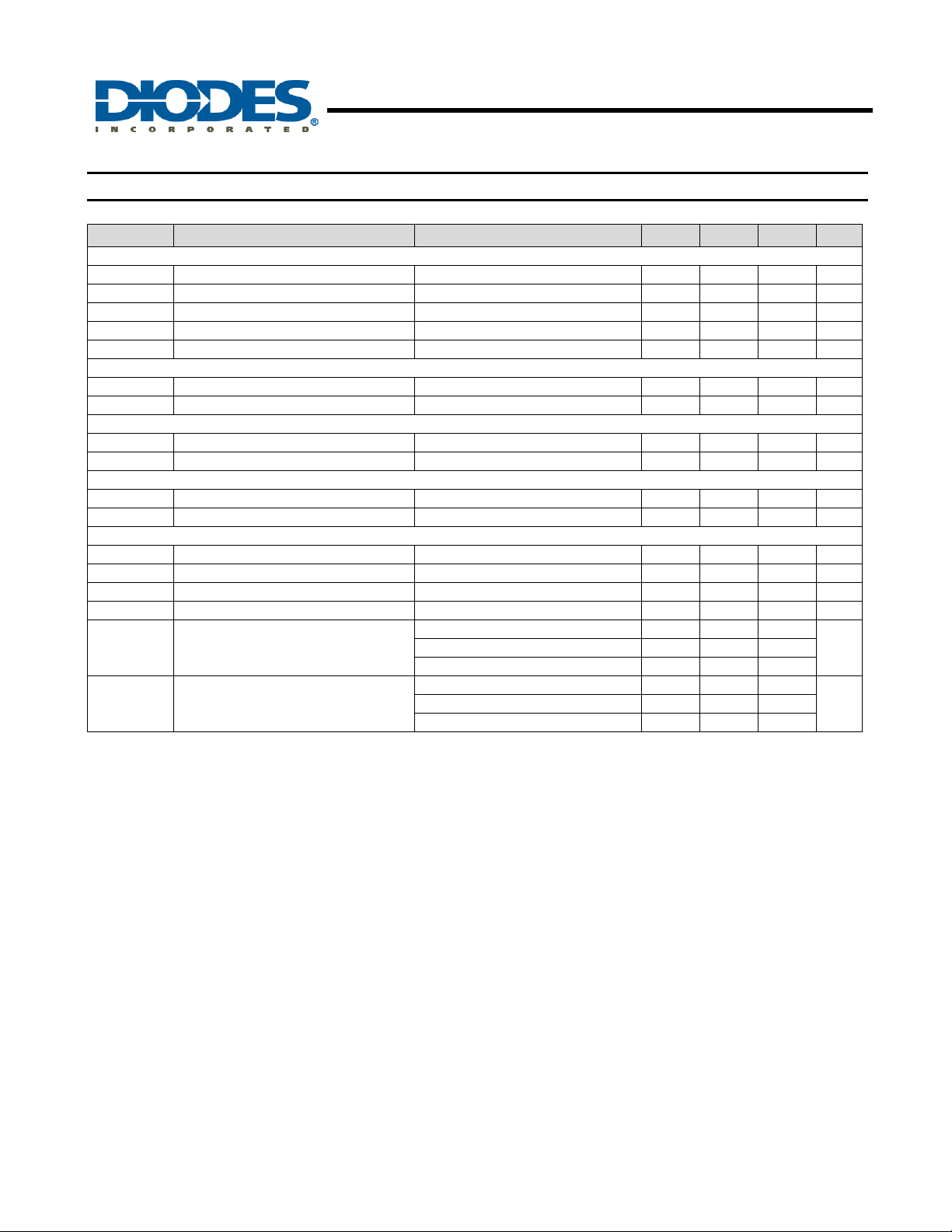
Electrical Characteristics (V
Symbol Parameter Conditions Min Typ. Max Unit
System Supply Input
VIN Operating Input Voltage 2.7 - 5.5 V
UVLO Under Voltage Lockout - 2.2 2.4 V
Under Voltage Lockout Hysteretic - 85 - mV
IQ Quiescent Current FB=0.35V, No Switching - 500 - μA
ISD Shutdown Current VEN < 0.4V - 0.1 1 μA
Oscillator
F
Operation Frequency 1 1.2 1.4 MHz
OSC
Dmax Maximum Duty Cycle 86 90 - %
Reference Voltage
VFB Feedback Voltage 0.225 0.25 0.275 V
IFB FB Pin Bias Current 10 45 100 nA
MOSFET
Rds(on) On Resistance of MOSFET - 0.95 1.2 Ω
I
Switching Current Limit Normal Operation - 750 - mA
OCP
Control and Protection
EN Voltage High ON 1.5 - - V
EN Voltage Low OFF - - 0.4 V
IEN EN Pin Pull Low Current - 4 6 μA
OVP OVP Threshold 26 30 34 V
θ
θ
Notes: 2. Test condition for SOT26, TSOT23-6 and DFN2020C-6: Device mounted on FR-4 substrate, single-layer PC board, 2oz copper,
Thermal Resistance Junction-to-
JA
Ambient
Thermal Resistance Junction-to-
JC
Case
with minimum recommended pad layout
= 3.6V, TA = 25°C, unless otherwise specified.)
IN
SOT26 (Note 2) 162
DFN2020C-6 (Note2) 200
SOT26 (Note 2) 36
DFN2020C-6 (Note 2) 30
o
C/WTSOT23-6 (Note 2) 152
o
C/WTSOT23-6 (Note 2) 32
AP5725
Document number: DS31844 Rev. 3 - 2
4 of 17
www.diodes.com
July 2010
© Diodes Incorporated
Page 5
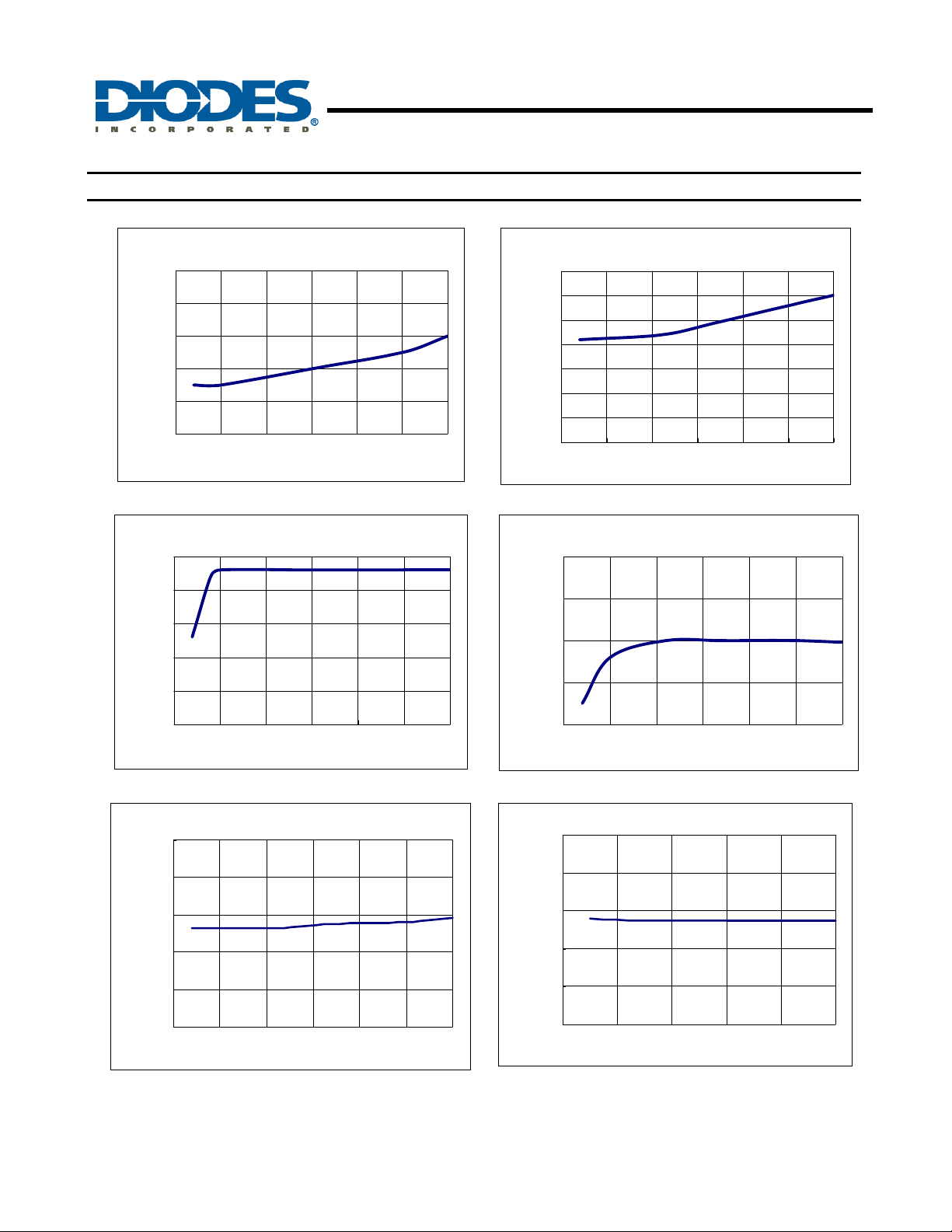
Typical Performance Characteristics (6 LEDs ; V
= 3.6V ; I
IN
AP5725
WHITE LED STEP-UP CONVERTER
= 25mA)
OUT
VIN vs. Shutdown Current
1
0.8
0.6
0.4
0.2
Shutdown Current(uA)
0
2.533.544.555.5
V
(V)
IN
VIN vs. Frequency
1.25
1.2
1.15
1.1
Frequency(MHz)
1.05
V
vs. Quiescent Current
IN
700
600
500
400
300
200
100
Quiescent Current(uA)
0
2.5 3 3.5 4 4.5 5 5.5
100
95
90
Max Duty(%)
85
V
(V)
IN
VIN vs. Max Duty
1
2.5 3 3.5 4 4.5 5 5.5
V
(V)
IN
VIN vs. Feed b ack V o lta g e
0.3
0.28
0.26
0.24
0.22
Feedback Vol tag e(V )
0.2
2.5 3 3.5 4 4.5 5 5.5
V
(V)
IN
80
2.533.544.555.5
I
vs. Feedback Voltage
OUT
0.3
0.28
0.26
0.24
0.22
Feedback V oltage(V)
0.2
0 1020304050
I
OUT
V
IN
(mA)
(V)
AP5725
Document number: DS31844 Rev. 3 - 2
5 of 17
www.diodes.com
July 2010
© Diodes Incorporated
Page 6
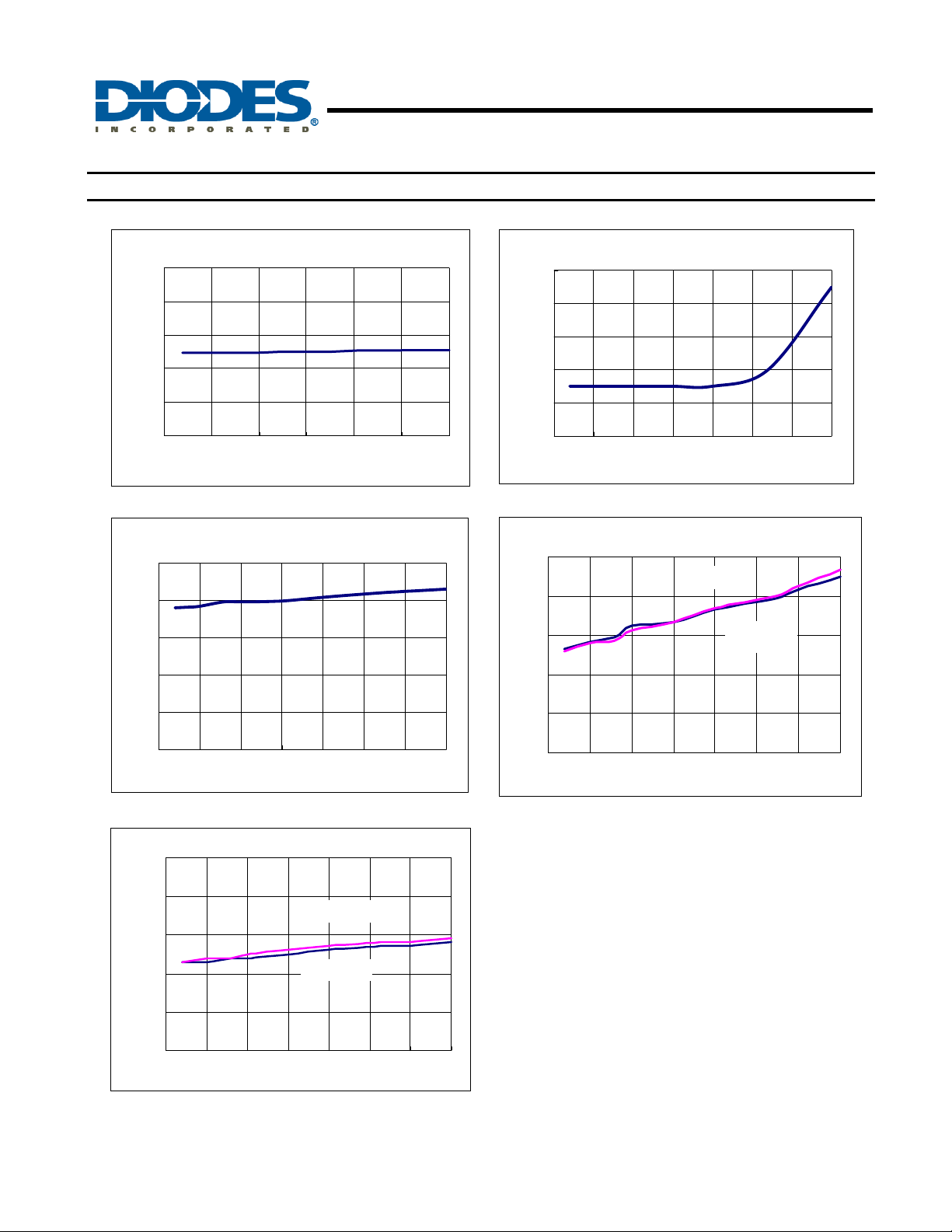
Typical Performance Characteristics (Continued)
AP5725
WHITE LED STEP-UP CONVERTER
VIN vs. O VP Threshold
35
33
31
29
27
OVP Threshold(V)
25
2.5 3 3.5 4 4.5 5 5.5
V
(V)
IN
Temperature vs. OVP Threshold
35
30
25
20
Temperature vs. Shutdown Current
1
0.8
0.6
0.4
0.2
Shutdown Current(uA)
0
-50 -25 0 25 50 75 100 125
Temperature (℃)
Temperature vs. Frequency
1.7
VIN = 4.2V
1.4
1.1
0.8
VIN = 3.6V
OVP Threshold(V)
15
10
-50 -25 0 25 50 75 100 125
Temperature (℃)
Frequency (MHZ)
0.5
0.2
-50 -25 0 25 50 75 100 125
Temperature (℃)
Tem perature vs. Fee dback Voltage
0.28
0.27
V
= 4.2V
IN
0.26
V
0.25
0.24
Feedback V o l tag e(V )
0.23
-50 -25 0 25 50 75 100 125
Temperature(℃)
= 3.6V
IN
AP5725
Document number: DS31844 Rev. 3 - 2
6 of 17
www.diodes.com
July 2010
© Diodes Incorporated
Page 7
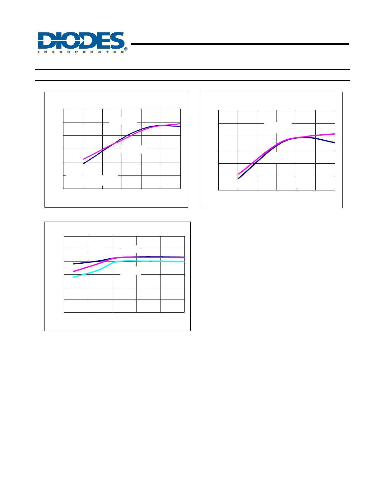
Typical Performance Characteristics (Continued)
I
vs. Efficiency
OUT
90
AP5725
WHITE LED STEP-UP CONVERTER
I
vs. Efficiency
OUT
90
85
80
75
70
Efficiency(%)
65
4 LEDs ; L = 22uH
60
0 5 10 15 20 25 30
100
90
80
70
60
Efficiency(%)
50
3 LEDs
V
= 4.2V
VIN = 3.6V
(mA)
I
OUT
V
vs. Efficiency
IN
4 LEDs
6 LEDs
85
80
75
70
Efficiency(%)
65
6 LEDs ; L = 22uH
60
0 5 10 15 20 25 30
VIN = 4.2V
VIN = 3.6V
(mA)
I
OUT
40
2.5 3 3.5 4 4.5 5
AP5725
Document number: DS31844 Rev. 3 - 2
VIN (V)
7 of 17
www.diodes.com
July 2010
© Diodes Incorporated
Page 8
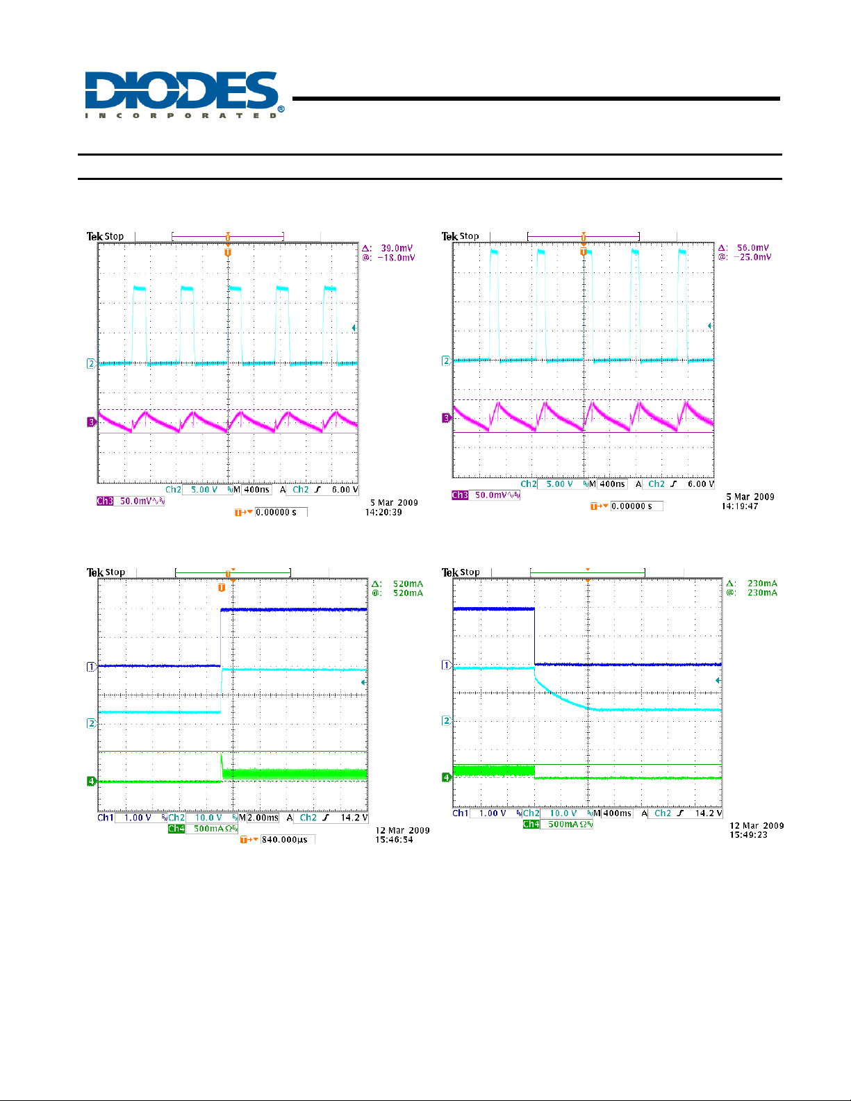
Typical Performance Characteristics (Continued)
Ripple
V
= 3.6V; 4 LEDs ; IOUT = 30mA
V
IN
OUT
AP5725
WHITE LED STEP-UP CONVERTER
V
Ripple
= 3.6V; 6 LEDs ; IOUT = 30mA
V
IN
OUT
SW SW
VOUT
V
OUT
POWER ON
= 3.6V; 6 LEDs ; IOUT = 30mA
V
IN
VEN
OUT
V
Irushi
VIN = 3.6V; 6 LEDs ; IOUT = 30mA
POWER OFF
VEN
OUT
V
Irushin
AP5725
Document number: DS31844 Rev. 3 - 2
8 of 17
www.diodes.com
July 2010
© Diodes Incorporated
Page 9
AP5725
WHITE LED STEP-UP CONVERTER
Applications Information
Inductor Selection
A 10μH~22μH inductor is recommended for most AP5725 applications. For high efficiency the inductor should
have low core losses at 1.2MHz and low DCR (copper wire resistance). The inductor saturation current rating
should also exceed the peak input current, especially for high load current applications (like 3S8P).
Capacitor Selection
The small size of ceramic capacitors are ideal for AP5725 applications. X5R and X7R types are recommended
because they retain their capacitance over wider voltage and temperature ranges than other types such as Y5V or
Z5U. A 1μF input capacitor and a 1μF output capacitor are sufficient for most AP5725 applications. For high
output current applications like 3S8P, larger output capacitor of 2.2uF ~ 4.7uF is recommended to minimize output
ripple.
Diode Selection
Schottky diodes, with their low forward voltage drop and fast reverse recovery, are the ideal choices for AP5725
applications. The forward voltage drop of a Schottky diode represents the conduction losses in the diode, while
the diode capacitance (C
or CD) represents the switching losses. For diode selection, both forward voltage drop
T
and diode capacitance need to be considered. Schottky diodes with higher current ratings usually have lower
forward voltage drop and larger diode capacitance, which can cause significant switching losses at the 1.2MHz
switching frequency of the AP5725. Schottky diodes with higher current ratings usually have lower forward voltage
drop and larger diode capacitance. Larger Schottky diode capacitance can cause significant switching losses at
the 1.2MHz switching frequency of the AP5725. A Schottky diode rated at 100mA to 200mA is sufficient for most
AP5725 applications.
LED Current Control
The LED current is controlled by the feedback resistor (R
LED current is 0.25V/ R
recommended). The formula and table for R
R
SET
= 0.25V/I
(See Table 1)
LED
. In order to have accurate LED current, precision resistors are preferred (1% is
SET
selection are shown below.
SET
in Figure 1). The feedback reference is 0.25V. The
SET
Table 1. R
I
LED
Resistor Value Selection
SET
(mA) R
SET
(Ω)
5 50
10 25
15 16.6
20 12.5
30 8.3
AP5725
Document number: DS31844 Rev. 3 - 2
9 of 17
www.diodes.com
July 2010
© Diodes Incorporated
Page 10
AP5725
WHITE LED STEP-UP CONVERTER
Applications Information (Continued)
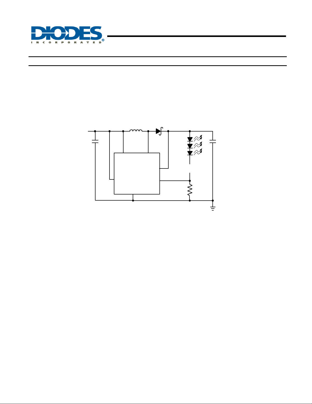
Open-Circuit Protection
In the cases of output open circuit, when the LEDs are disconnected from the circuit or the LEDs fail, the feedback
voltage will be zero. The AP5725 will then switch at a high duty cycle resulting in a high output voltage, which may
cause the SW and OVP pin voltage to exceed the voltage rating of these pins. The OVP pin monitors the output
voltage. If the output voltage reaches the over voltage protection threshold at the OVP pin (Figure 2), the over
voltage protection is activated and SW pin stops switching.
L1
V
IN
C
IN
22uH
1uF
D1
C
OUT
1uF
V
IN
SW
x
AP5725
EN
GND
Figure 2. LED Driver with Open-Circuit Protection
Dimming Control
There are four different types of dimming control circuits:
1. Using a PWM Signal to EN Pin
With the PWM signal applied to the EN pin, the AP5725 is turned on or off by the PWM signal. The LEDs operate
at either zero or full current. The average LED current increases proportionally with the duty cycle of the PWM
signal. A 0% duty cycle will turn off the AP5725 and corresponds to zero LED current. A 100% duty cycle
corresponds to full current. The typical frequency range of the PWM signal is below 2kHz.
OVP
FB
x
RSET
12
AP5725
Document number: DS31844 Rev. 3 - 2
10 of 17
www.diodes.com
July 2010
© Diodes Incorporated
Page 11
AP5725
WHITE LED STEP-UP CONVERTER
Applications Information (Continued)
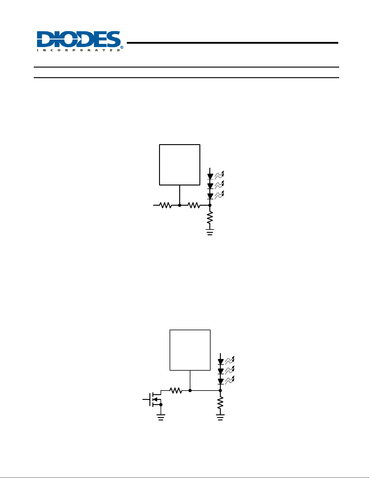
2. Using a DC Voltage
For some applications, the preferred method of brightness control is a variable DC voltage to adjust the
LED current. The dimming control using a DC voltage is shown in Figure 3. As the DC voltage increases, the
voltage drop on R2 increases and the voltage drop on R
selection of R2 and R3 will make the current from the variable DC source much smaller than the LED current and
much larger than the FB pin bias current. For V
dimming control of LED current from 0mA to 20mA.
range from 0V to 2V, the selection of resistors in Figure 3 gives
DC
AP5725
FB
decreases. Thus, the LED current decreases. The
SET
R3
100k
V
DC
R2
5k
RSET
12
Figure 3. Dimming Control Using a DC Voltage
3. Using a Filtered PWM Signal
The filtered PWM signal can be considered as an adjustable DC voltage. It can be used to replace the variable
DC voltage source in dimming control.
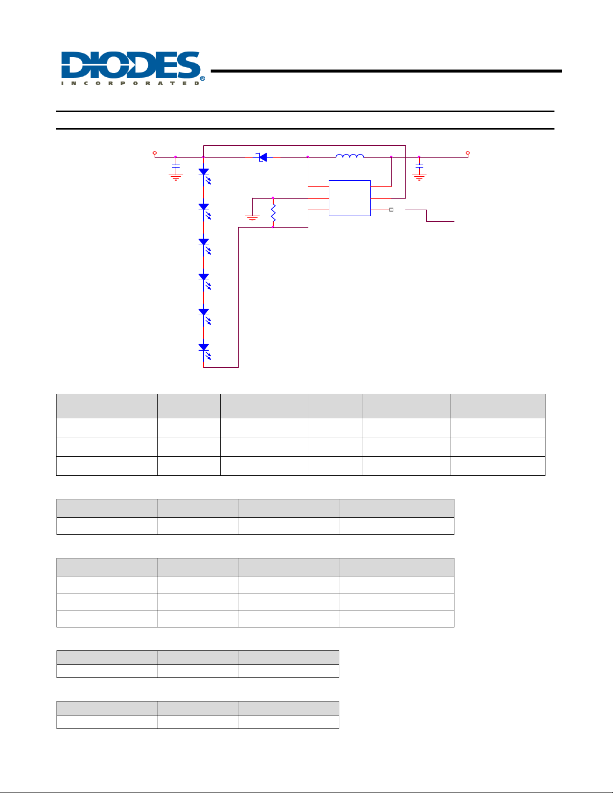
4. Using a Logic Signal
For applications that need to adjust the LED current in discrete steps, a logic signal can be used as shown in
Figure 4. R
increases when the NMOS is turned on.
sets the minimum LED current (when the NMOS is off). R
SET
sets how much the LED current
SET
AP5725
FB
AP5725
Document number: DS31844 Rev. 3 - 2
RINC
Logic
RSET
Signal
Figure 4. Dimming Control Using a Logic Signal
11 of 17
www.diodes.com
July 2010
© Diodes Incorporated
Page 12
Applications Information (Continued)
VOUT
C1
1uF
D2
LED
D3
LED
D4
LED
D5
LED
D6
LED
D7
LED
D1 B0540WS
R1
12ohm
1
2
3
AP5725
WHITE LED STEP-UP CONVERTER
VIN
L1 22uH
U1
SW
GND
FB
AP5725
Vin
OVP
EN
6
5
4
C2
1uF
ON OFF
Table 2. Suggested Inductors
Vendor
Inductors
(uH)
Current Rating
(A)
Type
Dimensions
(mm)
Series
Wurth Electronics 22 0.51A SMD 3.8X 3.8 X 1.6 744031220
GOTREND 22 0.56A SMD 3.8 X 3.8 X 1.05 GLP3810PH220N
TAIYO YUDRN 22 0.51A SMD 4.0 X 4.0 X 1.25 NR4012
Table 3. Suggested Capacitors for C
and C
IN
OUT
Vendor Capacitance Type Series
TAIYO YUDEN 1uF SMD TMK212 B7105MG-T
Table 4. Suggested Diodes
Vendor Rating Type Series
ZETEX 40V/0.5A SOD323 ZLLS400
DIODES 40V/0.5A SOD323 B0540WS
DIODES 40V/0.25A SOD523 SDM20U40
Table 5. Suggested Resistor
Vendor Type Series
YAGEO SMD FR-SK
Table 6. Suggested W-LED
Vendor Type Series
LITEON SMD LTW-C1911UC5
AP5725
Document number: DS31844 Rev. 3 - 2
12 of 17
www.diodes.com
July 2010
© Diodes Incorporated
Page 13
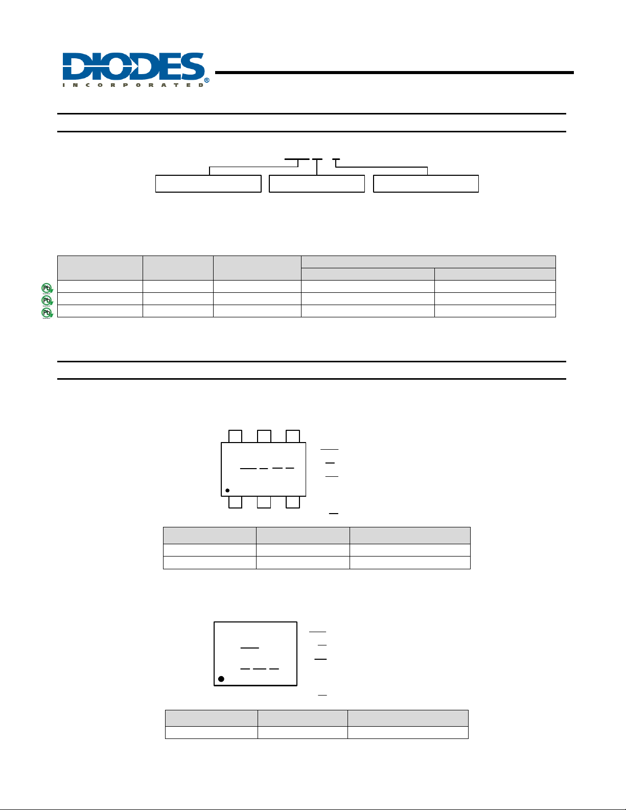
Ordering Information
AP 5725 XXX
AP5725
WHITE LED STEP-UP CONVERTER
G - 7
Package
W : SOT26
WU : TSOT23-6
FDC : DFN2020C-6
Green
G : Green
Packing
7 : Tape & Reel
Device
AP5725WG-7 W SOT26 3000/Tape & Reel -7
AP5725WUG-7 WU TSOT23-6 3000/Tape & Reel -7
AP5725FDCG-7 FDC DFN2020C-6 3000/Tape & Reel -7
Notes: 3. Pad layout as shown on Diodes Inc. suggested pad layout document AP02001, which can be found on our website at
http://www.diodes.com/datasheets/ap02001.pdf.
Package
Code
Packaging
(Note 3)
Quantity Part Number Suffix
7” Tape and Reel
Marking Information
(1) SOT26 and TSOT23-6
( Top View )
6
5
7
4
XX : Identification Code
Y
XX Y
WX
: Year 0~9
W : Week : A~Z : 1~26 week;
a~z : 27~52 week; z represents
1 2 3
52 and 53 week
X
: A~Z : Green
Part Number Package Identification Code
AP5725WG-7 SOT26 FC
AP5725WUG-7 TSOT23-6 GC
(2) DFN2020C-6
AP5725FDCG-7 DFN2020C-6 GC
AP5725
Document number: DS31844 Rev. 3 - 2
( Top View )
: Identification Code
XX
XX
Y W X
Part Number Package Identification Code
www.diodes.com
Y : Year : 0~9
W
: Week : A~Z : 1~26 w eek;
a~z : 27~52 week; z represents
52 and 53 week
X
: A~Z : Green
13 of 17
July 2010
© Diodes Incorporated
Page 14
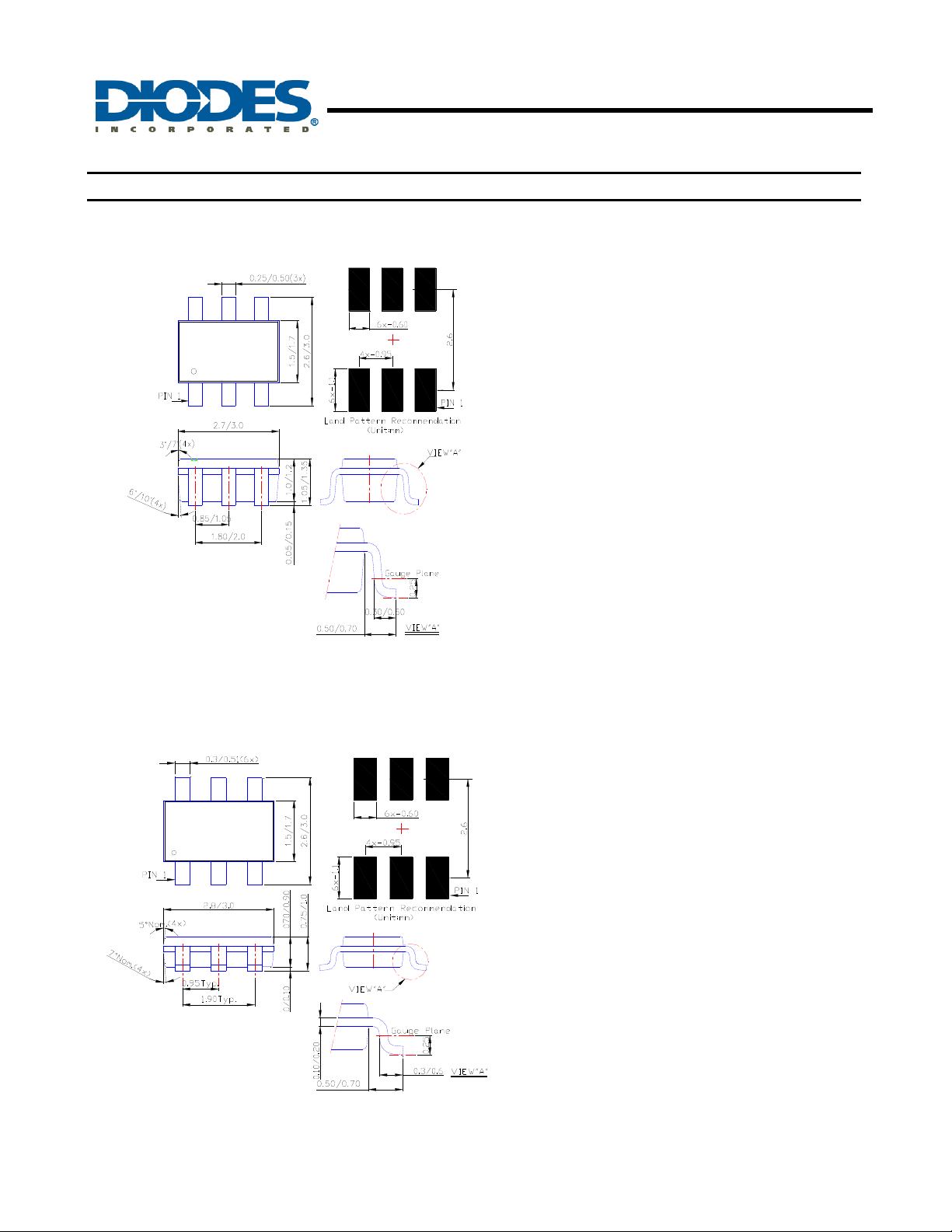
Package Outline Dimensions (All Dimensions in mm)
(1) Package Type: SOT26
AP5725
WHITE LED STEP-UP CONVERTER
(2) Package Type: TSOT23-6
AP5725
Document number: DS31844 Rev. 3 - 2
14 of 17
www.diodes.com
July 2010
© Diodes Incorporated
Page 15
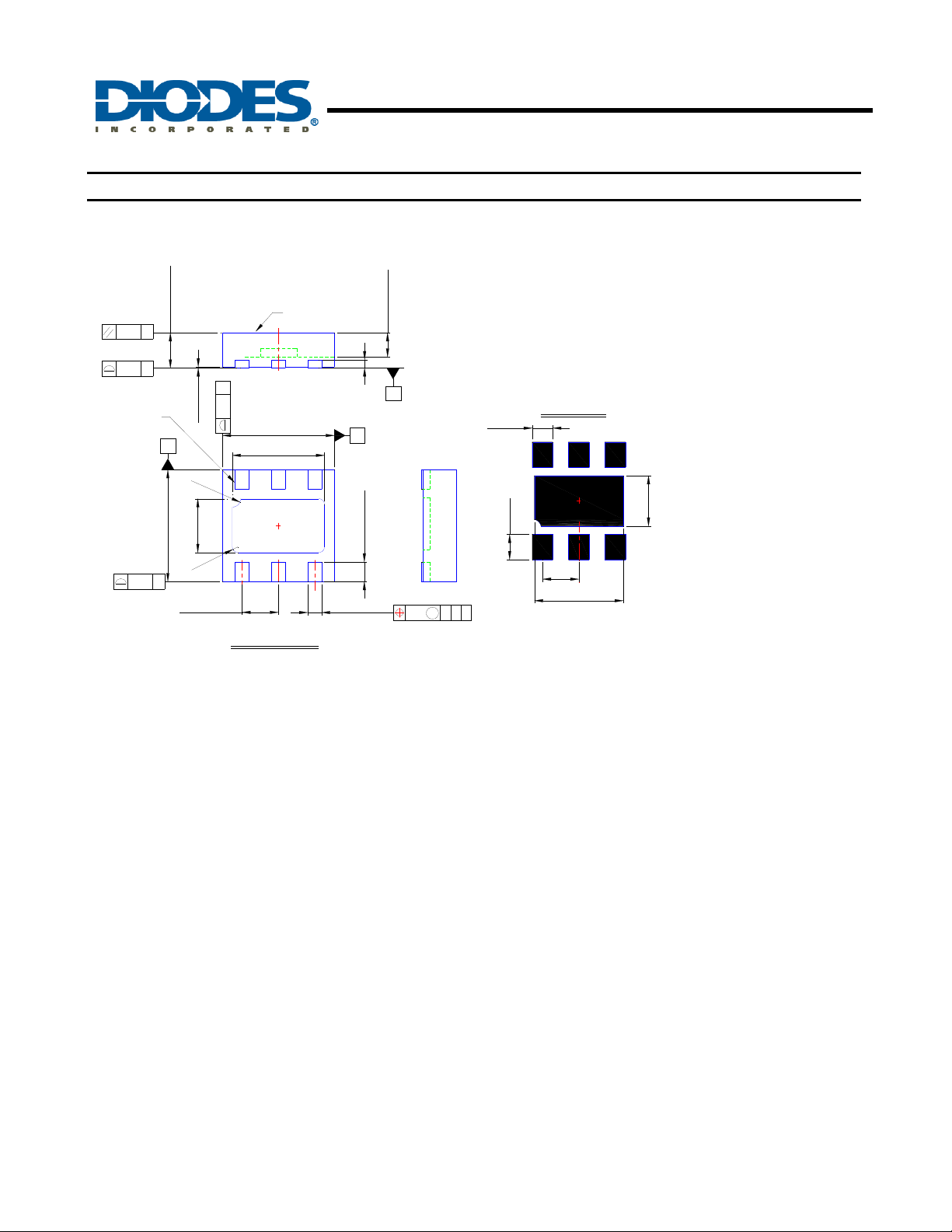
Package Outline Dimensions (Continued)
(3) Package Type: DFN2020C-6
AP5725
WHITE LED STEP-UP CONVERTER
Marking
1.95/2.075
1.55/1.75
0.15max.
A
0.25/0.35
0.25/0.35
0.43mon.
(Active area depth)
Seating plane
C
0.10
M C A B
0.37
Top View
0.9
0.45
0.65
1.59
Land Pattern Recommendation
(Unit:mm)
2x-
0.10 C
0.08 C
Pin#1 ID
0.25 B
0.57/0.63
0/0.05
B
R
0
0.86/1.06
1.95/2.075
0.1
R
0.65nom.
A
0.25
2x
.
1
5
Bottom View
AP5725
Document number: DS31844 Rev. 3 - 2
15 of 17
www.diodes.com
July 2010
© Diodes Incorporated
Page 16
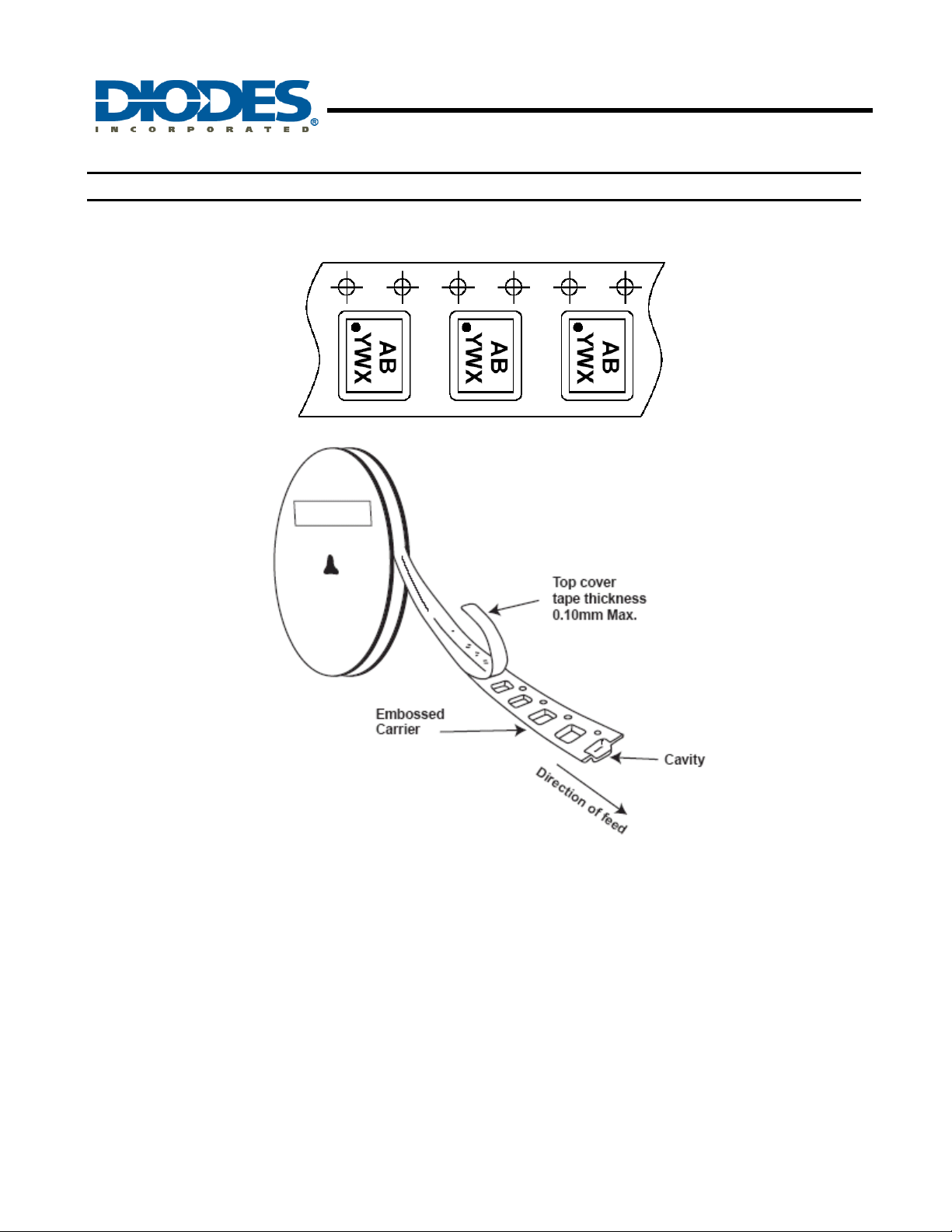
Taping Orientation
For DFN2020C-6
AP5725
WHITE LED STEP-UP CONVERTER
Notes: 4. The taping orientation of the other package type can be found on our website at http://www.diodes.com/datasheets/ap02007.pdf.
AP5725
Document number: DS31844 Rev. 3 - 2
16 of 17
www.diodes.com
July 2010
© Diodes Incorporated
Page 17

AP5725
WHITE LED STEP-UP CONVERTER
IMPORTANT NOTICE
DIODES INCORPORATED MAKES NO WARRANTY OF ANY KIND, EXPRESS OR IMPLIED, WITH REGARDS TO THIS
DOCUMENT, INCLUDING, BUT NOT LIMITED TO, THE IMPLIED WARRANTIES OF MERCHANTABILITY AND FITNESS FOR A
PARTICULAR PURPOSE (AND THEIR EQUIVALENTS UNDER THE LAWS OF ANY JURISDICTION).
Diodes Incorporated and its subsidiaries reserve the right to make modifications, enhancements, improvements, corrections or other
changes without further notice to this document and any product described herein. Diodes Incorporated does not assume any liability
arising out of the application or use of this document or any product described herein; neither does Diodes In corporated convey any
license under its patent or trademark rights, nor the rights of others. Any Customer or user of this documen t or products described
herein in such applications shall assume all risks of such use and will agree to hold Diodes Incorporated and all the companies
whose products are represented on Diodes Incorporated website, harmless against all damages.
Diodes Incorporated does not warrant or accept any liability whatsoever in respect of any products purchased through unauthorized
sales channel.
Should Customers purchase or use Diodes Incorporated products for any unintended or unauthorized application, Customers shall
indemnify and hold Diodes Incorporated and its representatives harmless against all claims, damages, expenses, and attorney fees
arising out of, directly or indirectly, any claim of personal injury or death associated with such unintended or unauthorized application.
Products described herein may be covered by one or more United States, international or foreign p atents pending. Product names
and markings noted herein may also be covered by one or more United States, international or foreign trademarks.
LIFE SUPPORT
Diodes Incorporated products are specifically not authorized for use as critical components in life support devices or systems without
the express written approval of the Chief Executive Officer of Diodes Incorporated. As used herein:
A. Life support devices or systems are devices or systems which:
1. are intended to implant into the body, or
2. support or sustain life and whose failure to perform when properly used in accordance with instructions for use provided
in the labeling can be reasonably expected to result in significant injury to the user.
B. A critical component is any component in a life support device or system whose failure to perform can be reasonably expected
to cause the failure of the life support device or to affect its safety or effectiveness.
Customers represent that they have all necessary expertise in the safety and regulatory ramifications of their life support dev ices or
systems, and acknowledge and agree that they are solely responsible for all legal, regulatory and safety-related requirements
concerning their products and any use of Diodes Incorporated products in such safety-critical, life support devices or systems,
notwithstanding any devices- or systems-related information or support that may be provided by Diodes Incorporated. Further,
Customers must fully indemnify Diodes Incorporated and its representatives against any damages arising out of the use of Diodes
Incorporated products in such safety-critical, life support devices or systems.
Copyright © 2010, Diodes Incorporated
www.diodes.com
AP5725
Document number: DS31844 Rev. 3 - 2
17 of 17
www.diodes.com
July 2010
© Diodes Incorporated
 Loading...