

Page 1
Universal AC input, Primary Side Regulation
AP3981D2 12V-1A EV Board User Guide
Parameter
Value
Input Voltage
90 to 264VAC
Input standby power
75mW
Main output Vo / Io
12V – 1A
Efficiency
~ 87%
Total Output Power
12W
Protections
OCP, OVP, OLP,OTP
XYZ Dimension
63 x 34 x 20 mm
ROHS Compliance
Yes
General Description
Based on Flyback topology, the Primary side
Regulated AP3981D2 EV board is designed to serve
as an example for High Efficiency, low cost & less
components consumer home appliance systems. Also
a 650V N MosFet is integrated within control IC for
easy fitting in a flexible & small size power system
design. During the valley on operating & work at PFM
region the high efficiency and low standby function can
be achieved, by mean of using multi-mode controlling
skill the accurate constant voltage and constant current
can be easy meet. Its output power is rated at 12W
with 12V-1A. It can meet DOE VI and CoC Tier 2
energy efficiency requirement.
Key Features
90 ~264VAC input range
Using the Primary side control for eliminating the Opto-
coupler.
Multi-Mode PFM method operations, the switching
frequency between 24kh ~80Khz.
With Valley on detection the switching stay at Valley on
region so that will improve power converting efficiency &
EMI performance, the 87% Efficiency can be reached at
full load.
During the burst mode operation and Low start-up
operating quiescent currents the 75mW low standby
input power can be achieved.
Dynamic response is improved during work at three
mode operation as well as benefiting the accurate
constant voltage (CV) regulation & constant current (CC)
performance.
There is a Soft start during startup process.
Built-in Jittering Frequency function which is the EMI
emission can be improved.
Internal Auto Recovery OCP, OVP, OLP, OTP Power
Protection, cycle by cycle current limit, also with DC
polarity protection
Built –in Cable Compensation mode.
With a Brown out Protection.
Universal AC input PSR 12V-1.0 A Power
Specifications (CV & CC mode)
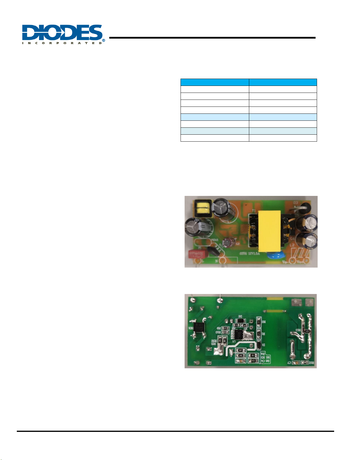
Evaluation Board Picture:
Figure 1: Top View
Applications
Switching AC-DC Adaptor & Charger
Power home Appliances systems
The auxiliary Vcc power supply for bigger power system.
AP3981D2 EV1 Page 1 of 12 10 – 25. 2018
Rev 1.0 www.diodes.com
Figure 2: Bottom View
Page 2
Universal AC input Primary side regulation
AP3981D2 12V-1A EV Board User Guide
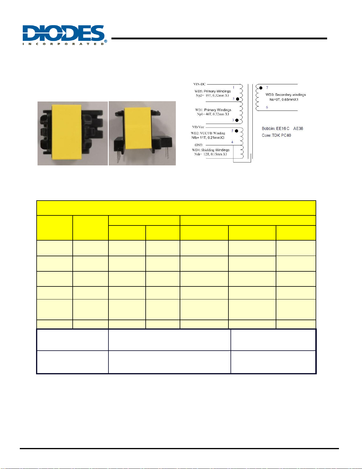
EE16C (Ae = 38mm^2)
NO
Winding
NAME
TERMINAL NO.
WINDING
START
FINISH
WIRE
TURNS
Layers
1
Na 5 4
Φ 0.21mm X 3
11 Ts
1
2
Np1
3 2 Φ 0.32mm X 1
46 Ts
2
3
Shield
4(GND)
NC
Φ 0.15mm X 1
12 Ts
1
4
Ns
7 6 Φ 0.65W X 1
9 Ts
1
5
Np2
2 1 Φ 0.32mm X 1
19 Ts
1
Primary Inductance
Pin 1-3,all other windings open,
measured at 10kHz, 0.4VRMS
1mH ± 7 %
Primary Leakage
Inductance
Pin 1-3, all other windings shorted,
measured at 10kHz, 0.4VRMS
80 uH (Max.)
AP3981D2 (90 VAC ~ 265VAC one outputs 12W Transformer Spec.)
1) Core& Bobbin:
EE16C, 5+2 pin 2)
Electrical Diagram:
3) Transformer Parameters
1. Primary Inductance (Pin1-Pin3), all other windings are open Lp =1 mH
± 7
% @10KHz
AP3981D2 EV1 Page 2 of 12 06 - 05 2019
Rev1.0 www.diodes.com
Page 3
Universal AC input Primary side regulation
AP3981D2 12V-1A EV Board User Guide
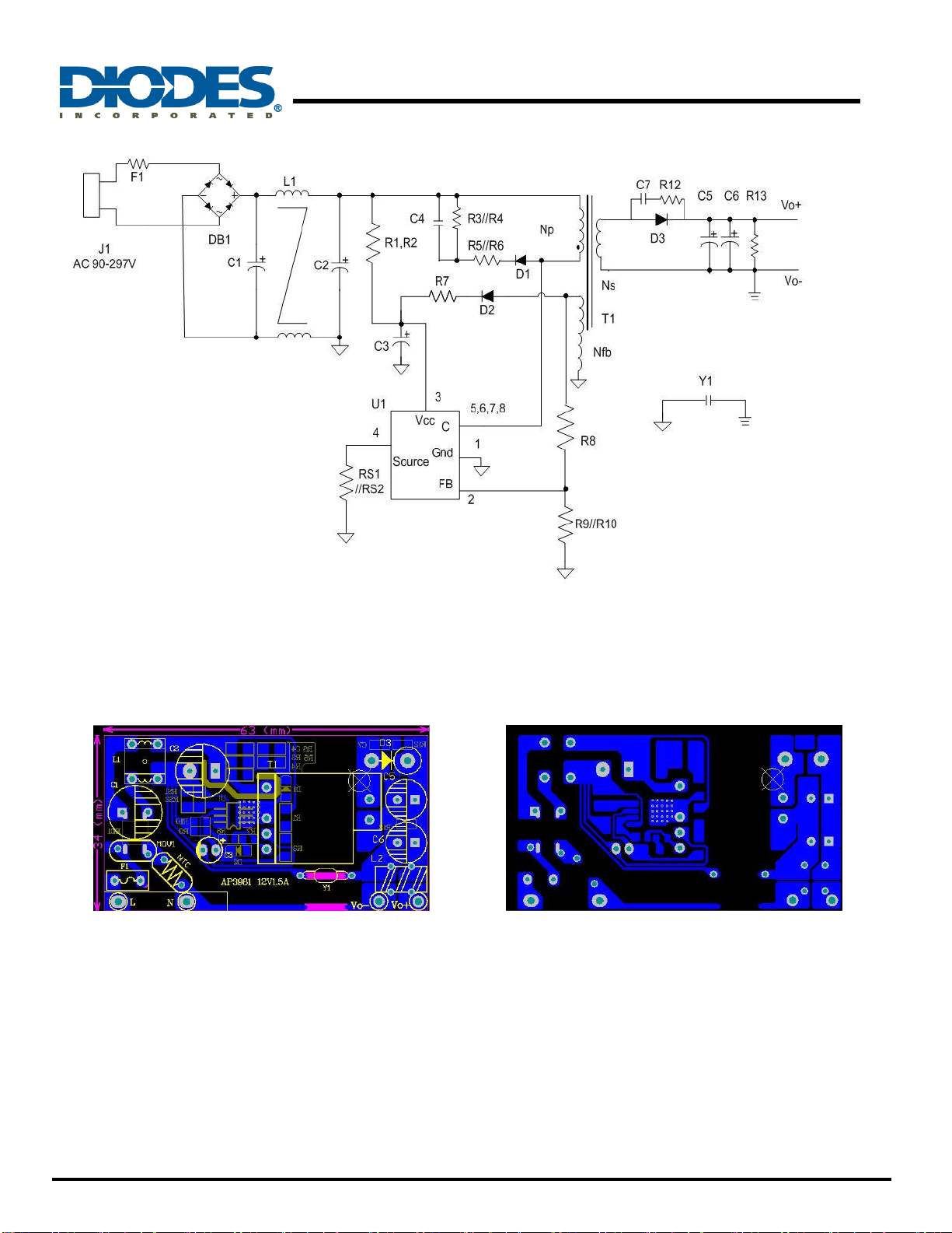
Evaluation Board Schematic
Figure 3: Evaluation Board Schematic
Evaluation Board PCB Layout
Figure4: PCB Board Layout Top View Figure5: PCB Board Layout Bottom View
AP3981D2 EV1 Page 3 of 12 06 - 05 2019
Rev1.0 www.diodes.com
Page 4
Universal AC input Primary side regulation
AP3981D2 12V-1A EV Board User Guide
AP3981D2 12V-1A BOM 8-28-2018
Item
QTY per
board
REF. DES. Description MFG or Supplier
MFG P/N or Supplier P/N
Digi key #
0
1 1 C1
10uf /400V 8 x 18mm Aishi Electro
2 1 C2
10uf /400V 8 x 18mm Aishi Electro
3 1 C3
4.7uF/50V 5 x 10mm Aishi Electro
4 1 C4
470pf / 200V, 0805 X7R Holy Stone
5 1 C5
470uf /16V 8 x 12mm Rubycon Electro
6 1 C6
470uf /16V 8 x 12mm Rubycon Electro
7 1 C7
470pf / 200V, 0805 X7R Holy Stone
8 1 R1
1.6M ohm 1206 Yageo
9 1 R2
1.6M ohm 1206 Yageo
10 1 R3
360K ohm 1206 Yageo
11 1 R4
360K ohm 1206 Yageo
12 1 R5
300R ohm 1206 Yageo
13 1 R6
300R ohm 1206 Yageo
14 1 R7
2.7R ohm 0805 Yageo
15 1 R8
30.1K ohm 0805 Yageo
16 1 R9
6.19K ohm 0805 Yageo
17 1 R10
300K ohm 0805 Yageo
18 1 RS1
1.8R ohm 1206 Yageo
19 1 RS2
1.8R ohm 1206 Yageo
20 1 R12
20R ohm 0805 Yageo
21 1 R13
12K ohm 1206 Yageo
22 1 BD1
ABS10 Diodes
23 1 D1
D7(1N4007) Diodes
24 1 D2
F7(FR107) Diodes
25 1 D3
SR5100L JF
26 1 F1
2A Fuse
27 1 L1
10mH Inductor
28 1 Y1
470pf/250Vac Y1 Holy Stone
29 1 U1
AP3981D2 sop-8 Diodes
AP3981D2 12V-1A BOM 8-28-2018
Quick Start Guide
1. The evaluation board is preset at 12V/1A from output + & -
2. Ensure that the AC source is switched OFF or disconnected before doing connection.
3. Connect the AC line wires of power supply to “L and N” on the left side of the board.
4. Turn on the AC main switch.
5. Measure Red & Black wires to ensure correct output voltages at 12V respectively.
Build of Material
AP3981D2 EV1 Page 4 of 12 06 - 05 2019
Rev1.0 www.diodes.com
Page 5
Universal AC input Primary side regulation
AP3981D2 12V-1A EV Board User Guide
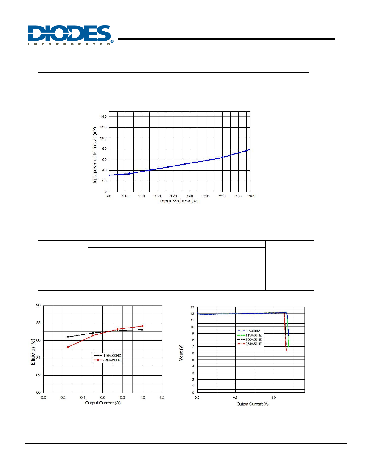
Input Voltage
115Vac/60Hz
230Vac/50Hz
Note
Pin (w)
34mW
64mW
At no loading
AC input
Efficiency (%)
Eff_avg at four
conditions
10%
25%
50%
75%
100%
90VAC/60Hz
115VAC/60Hz
84.01%
86.42%
86.85%
87.13%
87.24%
86.91%
230VAC/50Hz
80.08%
85.24%
86.56%
87.28%
87.62%
86.67%
264VAC/50Hz
Eff_avg
80
81
82
83
84
85
86
87
88
0.375 0.75 1.125 1.5
115vac
230Vac
output current
Input & Output Characteristics
Input Standby Power
Figure 6: The Efficiency curve with at different AC input
Input power Efficiency at different loading
Figure 7: The efficiency curve with different loading Figure 8: CV & CC Curve at OCP set poits
AP3981D2 EV1 Page 5 of 12 06 - 05 2019
Rev1.0 www.diodes.com
Page 6
Universal AC input Primary side regulation
AP3981D2 12V-1A EV Board User Guide
AC input
90VAC
115VAC
230VAC
264VAC
Note
I _max
1.19 A
1.18A
1.16A
1.16A
AC input Voltage
90VAC/60Hz
115VAC/60Hz
230VAC/50Hz
265VAC/50Hz
Note
12.00Vo
12.27V/1A
12.29V/1A
12.33V/1A
12.34V/1A
0.58%<1%
AC input Voltage
115VAC/60Hz
230VAC/50Hz
12V Full Load
12.288V / 1A
12.322V/1A
12V 10% of FL
11.88V /0.1A
11.884V/0.1A
Note: cable
compensation
3.4%
3.65%
OCP Current set point with at different AC line
PSU Output Characteristics:
Line Regulation (at full loading condition):
Cross Load Regulation (at nominal line AC input voltage):
Note: All output voltages are measured at output PCB board Edge. Internal Cable Compensation 8%
Key Performance Waveforms:
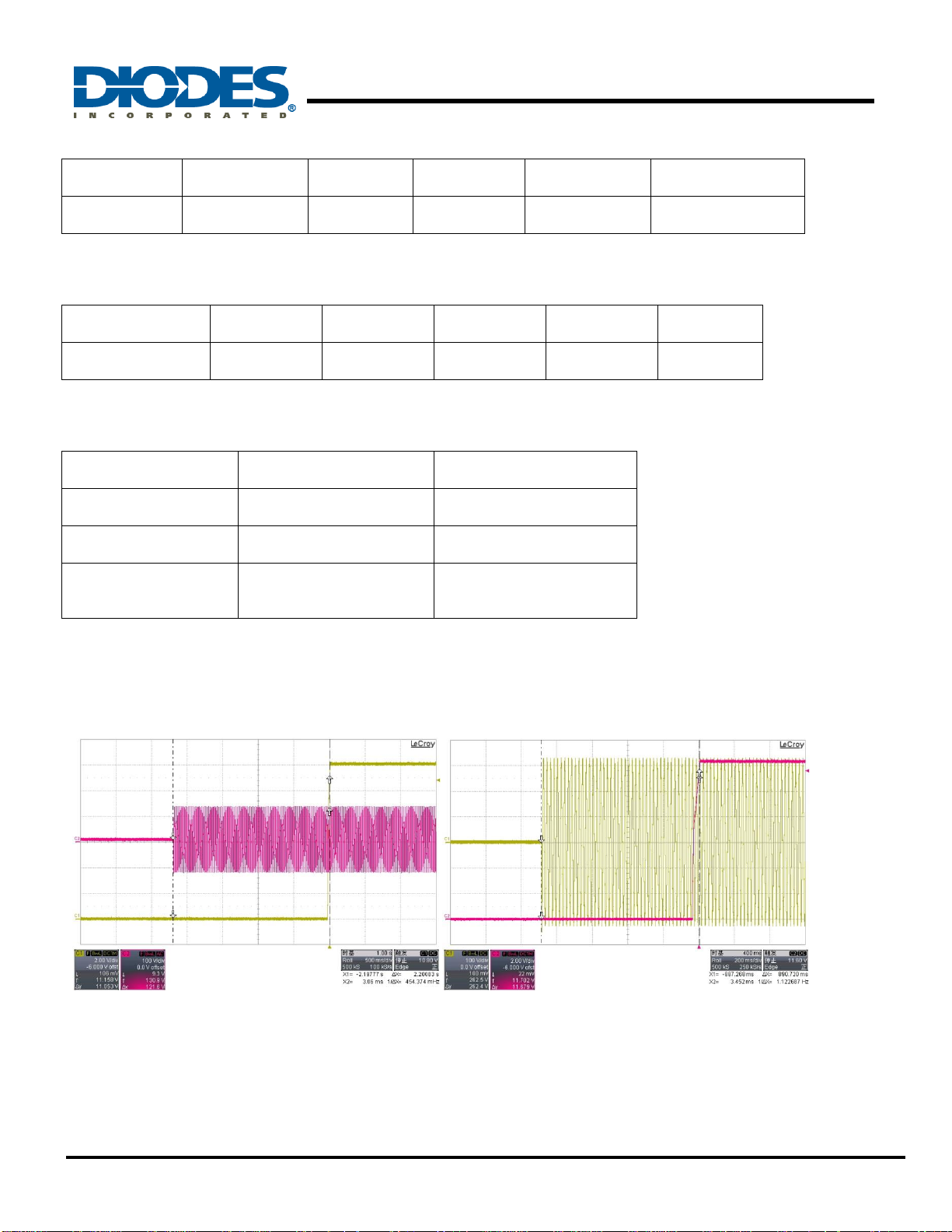
System start - up time
Figure 9:AP3981D2 turn on time 2.2sFL at 90Vac Figure 10: AP3981D2 turn on time 0.89s at FL, at 230Vac
AP3981D2 EV1 Page 6 of 12 06 - 05 2019
Rev1.0 www.diodes.com
Page 7
Universal AC input Primary side regulation
AP3981D2 12V-1A EV Board User Guide
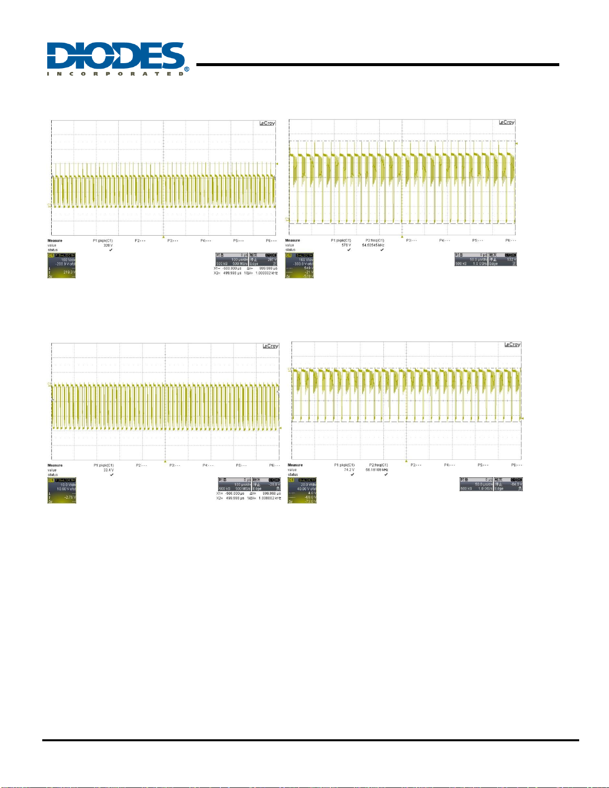
System main switching Voltage Stress on AP3981D2 Pin 5,6,7,8
Figure 11:AP3981D Vds at FL at 90Vac Vds=320Vp-p Figure 12: AP3981D Vds at FL at 264Vac, Vds=576Vp-p
System Voltage Stress across on U2 D-S
Figure 13: D3 D-S voltage stress at 90Vac FL Figure 14: D3 D-S voltage stress at 264Vac at FL
Vd3 d_S = 33.4Vp-p 10V/div Vd3 d_S = 74.2Vp-p 20V/div
AP3981D2 EV1 Page 7 of 12 06 - 05 2019
Rev1.0 www.diodes.com
Page 8
Universal AC input Primary side regulation
AP3981D2 12V-1A EV Board User Guide
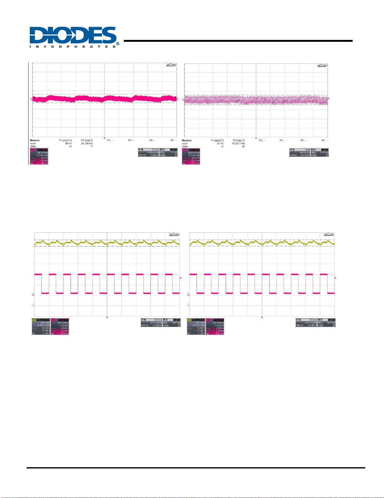
System output Ripple performance
Figure 15: The Ripple at 90Vac_in Vpp=86mv FL Figure 16: The Ripple at 264Vac_in Vpp=51mv FL
System Dynamic Response performance
Figure 17: 90VAC; Load level: 0.1~1A; Vout: 12.58~11.34V Figure 18: 264VAC; Load level: 0.1~1A; Vout: 12.60~11.4V
Frequency: 10ms~10mS. Slew rate: 0.25A/us Frequency: 10ms~10mS. Slew rate: 0.25A/us
AP3981D2 EV1 Page 8 of 12 06 - 05 2019
Rev1.0 www.diodes.com
Page 9
Universal AC input Primary side regulation
AP3981D2 12V-1A EV Board User Guide
System Dynamic Response performance
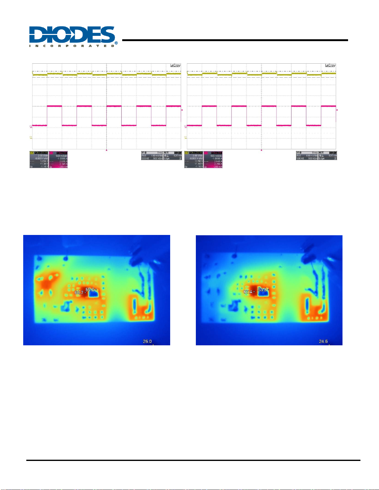
Figure 19: 90VAC; Load level: 0.1~1A; Vout: 12.58~11.38V Figure 20: 264VAC; Load level: 0.1~1A; Vout: 12.56~11.4V
Frequency: 100ms~100mS. Slew rate: 0.25A/us Frequency: 100ms~100mS. Slew rate: 0.25A/us
Thermal Test data at room Temperature after running after 1 hr
Figure21 Figure22:
Ta 26℃ Ta 24.6℃
U1 AP3981D2 63.7℃ U1 AP3981D2 67.4℃
AP3981D2 EV1 Page 9 of 12 06 - 05 2019
Rev1.0 www.diodes.com
Page 10
Universal AC input Primary side regulation
AP3981D2 12V-1A EV Board User Guide
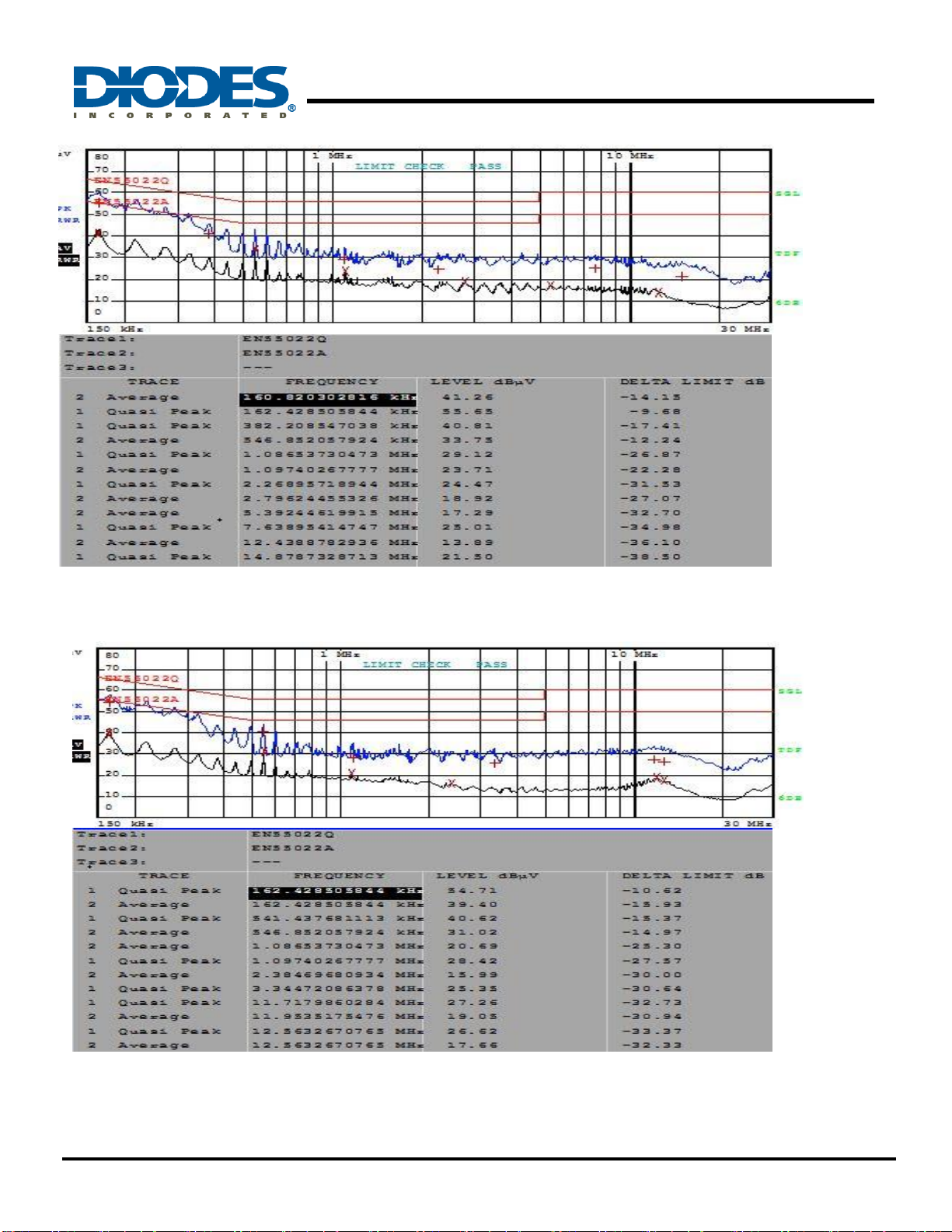
System EMI L-Line Scan Data
Figure 23: EMI Scan at 230Vac
System EMI N-Line Scan Data
Figure 24: EMI Scan at 230Vac
AP3981D2 EV1 Page 10 of 12 06 - 05 2019
Rev1.0 www.diodes.com
Page 11

Universal AC input Primary side regulation
AP3981D2 12V-1A EV Board User Guide
Please see the recommand Application note for reference
(web page - http://www.diodes.com/appnote_dnote.html)
AP3981D2 EV1 Page 11 of 12 06 - 05 2019
Rev1.0 www.diodes.com
Page 12

Universal AC input Primary side regulation
AP3981D2 12V-1A EV Board User Guide
IMPORTANT NOTICE
DIODES INCORPORATED MAKES NO WARRANTY OF ANY KIND, EXPRESS OR IMPLIED, WITH REGARDS TO
THIS DOCUMENT, INCLUDING, BUT NOT LIMITED TO, THE IMPLIED WARRANTIES OF MERCHANTABILITY
AND FITNESS FOR A PARTICULAR PURPOSE (AND THEIR EQUIVALENTS UNDER THE LAWS OF ANY
JURISDICTION).
Diodes Incorporated and its subsidiaries reserve the right to make modifications, enhancements, improvements, corrections or
other changes without further notice to this document and any product described herein. Diodes Incorporated does not assume any
liability arising out of the application or use of this document or any product described herein; neither does Diodes Incorporated
convey any license under its patent or trademark rights, nor the rights of others. Any Customer or user of this document or
products described herein in such applications shall assume all risks of such use and will agree to hold Diodes Incorporated and all
the companies whose products are represented on Diodes Incorporated website, harmless against all damages.
Diodes Incorporated does not warrant or accept any liability whatsoever in respect of any products purchased through
unauthorized sales channel.
Should Customers purchase or use Diodes Incorporated products for any unintended or unauthorized application, Customers shall
indemnify and hold Diodes Incorporated and its representatives harmless against all claims, damages, expenses, and attorney
fees arising out of, directly or indirectly, any claim of personal injury or death associated with such unintended or unauthorized
application.
Products described herein may be covered by one or more United States, international or foreign patents pending. Product names
and markings noted herein may also be covered by one or more United States, international or foreign trademarks.
This document is written in English but may be translated into multiple languages for reference. Only the English version of this
document is the final and determinative format released by Diodes Incorporated.
LIFE SUPPORT
Diodes Incorporated products are specifically not authorized for use as critical components in life support devices or systems
without the express written approval of the Chief Executive Officer of Diodes Incorporated. As used herein:
A. Life support devices or systems are devices or systems which:
1. are intended to implant into the body, or
2. support or sustain life and whose failure to perform when properly used in accordance with instructions for
use provided in the labeling can be reasonably expected to result in significant injury to the user.
B. A critical component is any component in a life support device or system whose failure to perform can be reasonably expected
to cause the failure of the life support device or to affect its safety or effectiveness.
Customers represent that they have all necessary expertise in the safety and regulatory ramifications of their life support devices or
systems, and acknowledge and agree that they are solely responsible for all legal, regulatory and safety-related requirements
concerning their products and any use of Diodes Incorporated products in such safety-critical, life support devices or systems,
notwithstanding any devices- or systems-related information or support that may be provided by Diodes Incorporated. Further,
Customers must fully indemnify Diodes Incorporated and its representatives against any damages arising out of the use of Diodes
Incorporated products in such safety-critical, life support devices or systems.
Copyright © 2016, Diodes Incorporated
www.diodes.com
AP3981D2 EV1 Page 12 of 12 06 - 05 2019
Rev1.0 www.diodes.com
 Loading...