

Page 1
Data Sheet
340kHz, 3A Synchronous DC-DC Buck Converter AP3503
General Description
The AP3503 is a 340kHz fixed frequency, current
mode, PWM synchronous buck (step-down) DC-DC
converter, capable of driving a 3A load with high
efficiency, excellent line and load regulation. The
device integrates N-channel power MOSFET
switches with low on-resistance. Current mode
control provides fast transient response and
cycle-by-cycle current limit.
The AP3503 employs complete protection to ensure
system security. Including output Over Voltage
Protection, input Under Voltage LockOut,
programmable soft-start, Over Temperature
Protection to safeguard the circuit.
This IC is available in PSOP-8 package.
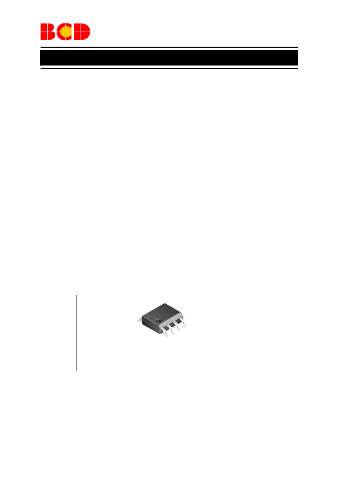
Figure 1. Package Type of AP3503
PSOP-8
Features
• Input Voltage Range: 4.5V to 18V
• Fixed 340kHz Frequency
• High Efficiency: up to 95%
• Output Current: 3A
• Current Mode Control
• Built-in Over Current Protection
• Built-in Thermal Shutdown Function
• Built-in UVLO Function
• Built-in Over Voltage Protection
• Programmable Soft-start
Applications
• LCD TV
• Set Top Box
• Portable DVD
• Digital Photo Frame
May. 2012 Rev. 1. 7 BCD Semiconductor Manufacturing Limited
1
Page 2
Data Sheet
340kHz, 3A Synchronous DC-DC Buck Converter AP3503
Pin Configuration
MP Package
(PSOP-8)
1
2
3
4
8
7
6
5
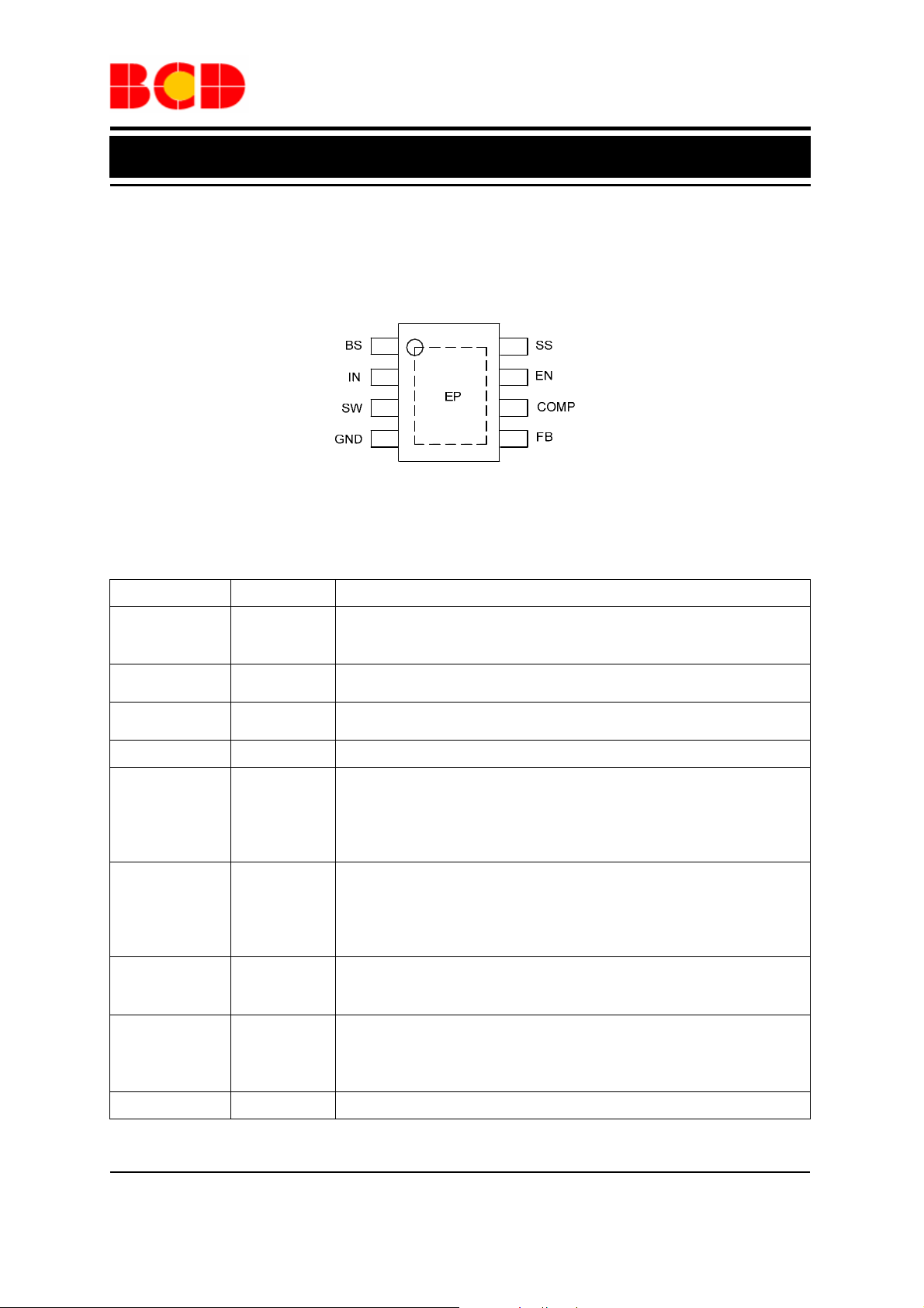
Figure 2. Pin Configuration of AP3503 (Top View)
Pin Description
Pin Number Pin Name Function
Bootstrap pin. A bootstrap capacitor is connected between the BS pin
1
2
3
4
5
6
7
8
BS
and SW pin. The voltage across the bootstrap capacitor drives the
internal high-side power MOSFET
IN
SW
Supply power input pin. A capacitor should be connected between the
IN pin and GND pin to keep the input voltage constant
Power switch output pin. This pin is connected to the inductor and
bootstrap capacitor
GND Ground pin
Feedback pin. This pin is connected to an exte rnal resistor divider to
program the system output voltage. When the FB pin voltage exceeds
FB
1.1V, the over voltage protection is triggered. When the FB pin
voltage is below 0.3V, the oscillator frequency is lowered to realize
short circuit protection
Compensation pin. This pin is the output of the transconductance
error amplifier and the input to the current comparator. It is used to
COMP
compensate the control loop. Connect a series RC network from this
pin to GND. In some cases, an additional capacitor from this pin to
GND pin is required
Control input pin. EN is a digital in put that turns the regulator on or
EN
off. Drive EN high/low to turn on/off the regulator. Pull up with
100kΩ resistor for automatic startup
Soft-start control input pin. SS controls the soft-start period. Connect
SS
a capacitor from SS to GND to set the soft-start period. A 0.1µF
capacitor sets the soft-start period to 15ms. To disable the soft-start
feature, leave SS unconnected
EP Exposed pad. It should be connected to GND in PCB layout
May. 2012 Rev. 1. 7 BCD Semiconductor Manufacturing Limited
2
Page 3
Data Sheet
340kHz, 3A Synchronous DC-DC Buck Converter AP3503
Functional Block Diagram
2
IN
EN
7
1.5V
SHUTDOWN
COMPARATOR
0.3V
LOCK
COMPARATOR
SCP
INTERNAL
REGULATOR
OSCILLATOR
90k/340k
CLK
VA
VB
SLOP
COMP
CURRENT
SENSE
AMPLIFIER
PWM
COMPARATOR
VA
+
1
BS
M1
Q
S
Q
R
M2
3
SW
2.5 V
SS
VB
6
8
A
EA
5
FB
0.
925V
6
COMP
1.3V
4
GND
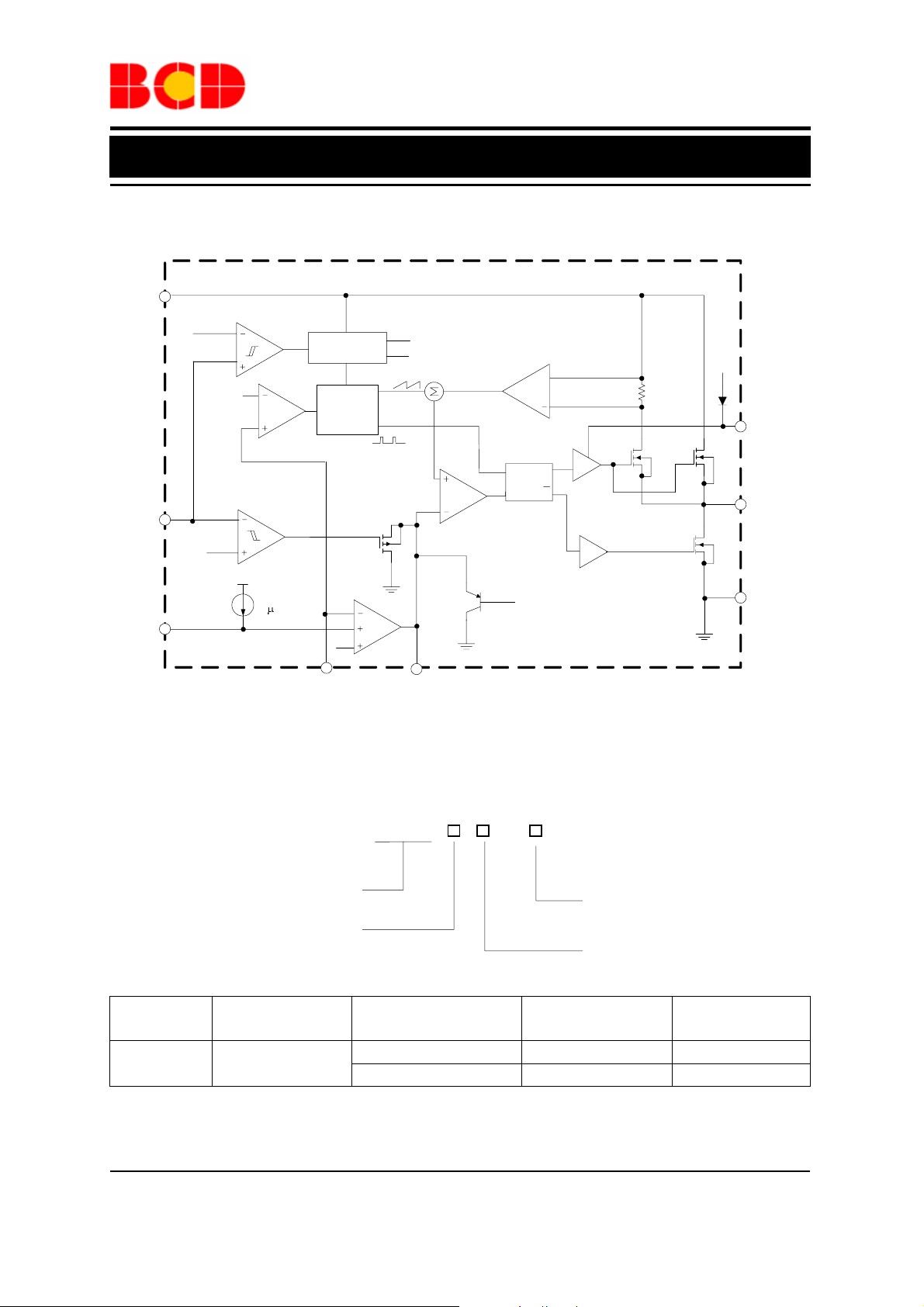
Figure 3. Functional Block Diagram of AP3503
Ordering Information
AP3503 -
Package
Temperature
PSOP-8
Circuit Type
Package
MP: PSOP-8
Range
-40 to 85°C
Part Number Marking ID Packing Type
AP3503MP-G1 3503MP-G1 Tube
AP3503MPTR-G1 3503MP-G1 Tape & Reel
G1: Green
TR: Tape & Reel
Blank: Tube
BCD Semiconductor's Pb-free products, as designated with "G1" suffix in the part number, are RoHS compliant
and green.
May. 2012 Rev. 1. 7 BCD Semiconductor Manufacturing Limited
3
Page 4
Data Sheet
340kHz, 3A Synchronous DC-DC Buck Converter AP3503
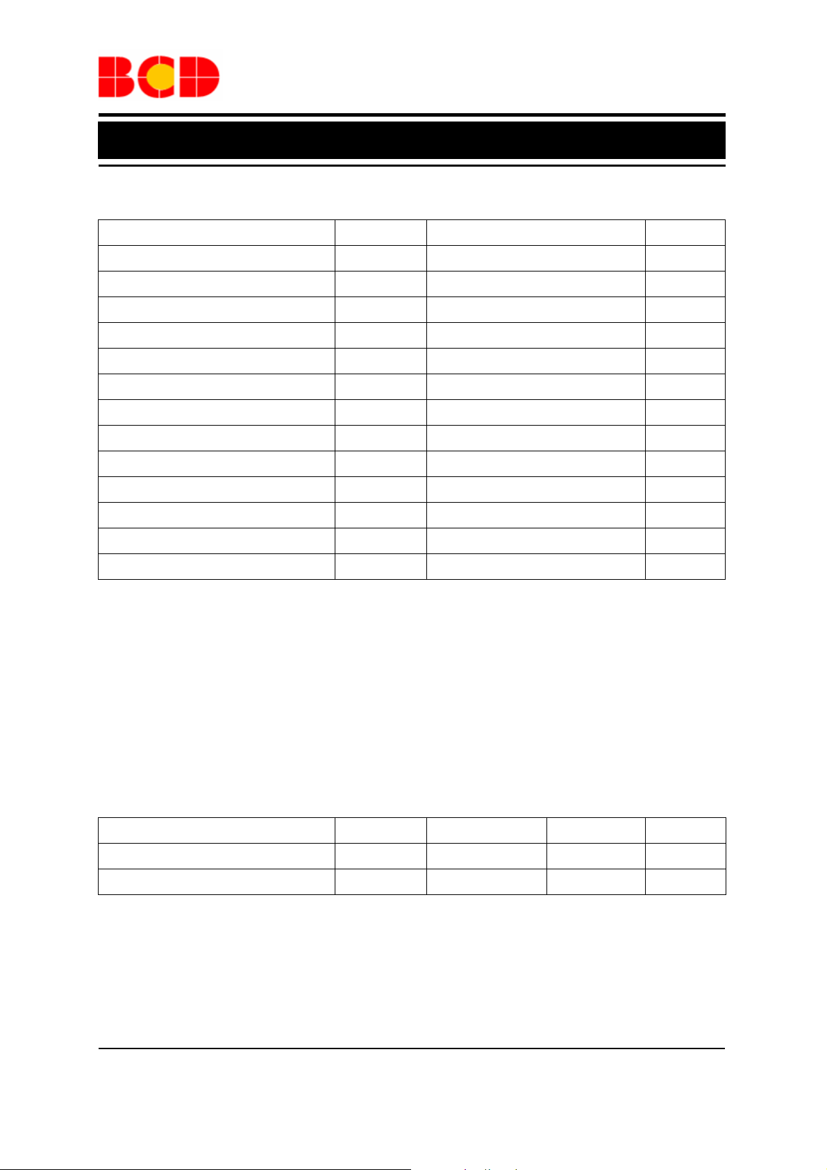
Absolute Maximum Ratings (Note 1)
Parameter Symbol Value Unit
IN Pin Voltage VIN -0.3 to 20 V
EN Pin Voltage VEN -0.3 to VIN V
SW Pin Voltage VSW 21 V
BS Pin Voltage VBS -0.3 to VSW+6 V
FB Pin Voltage VFB -0.3 to 6 V
COMP Pin Voltage V
SS Pin Voltage VSS -0.3 to 6 V
Thermal Resistance
Operating Junction Temperature TJ 150 ºC
Storage Temperature T
Lead Temperature (Soldering, 10sec) T
ESD (Human Body Model) VHBM 2000 V
ESD (Machine Model) VMM 200 V
-0.3 to 6 V
COMP
θ
JA
-65 to 150 ºC
STG
260 ºC
LEAD
60 ºC/W
Note 1: Stresses greater than those listed under “Absolute Maximum Ratings” may cause permanent damage to
the device. These are stress ratings only, and functional operation of the device at these or any other conditions
beyond those indicated under “Recommended Operating Conditions” is not implied. Exposure to “Absolute
Maximum Ratings” for extended periods may affect device reliability.
Recommended Operating Conditions
Parameter Symbol Min Max Unit
Input Voltage VIN 4.5 18 V
Operating Ambient Temperature TA -40 85 ºC
May. 2012 Rev. 1. 7 BCD Semiconductor Manufacturing Limited
4
Page 5
µ
Data Sheet
340kHz, 3A Synchronous DC-DC Buck Converter AP3503
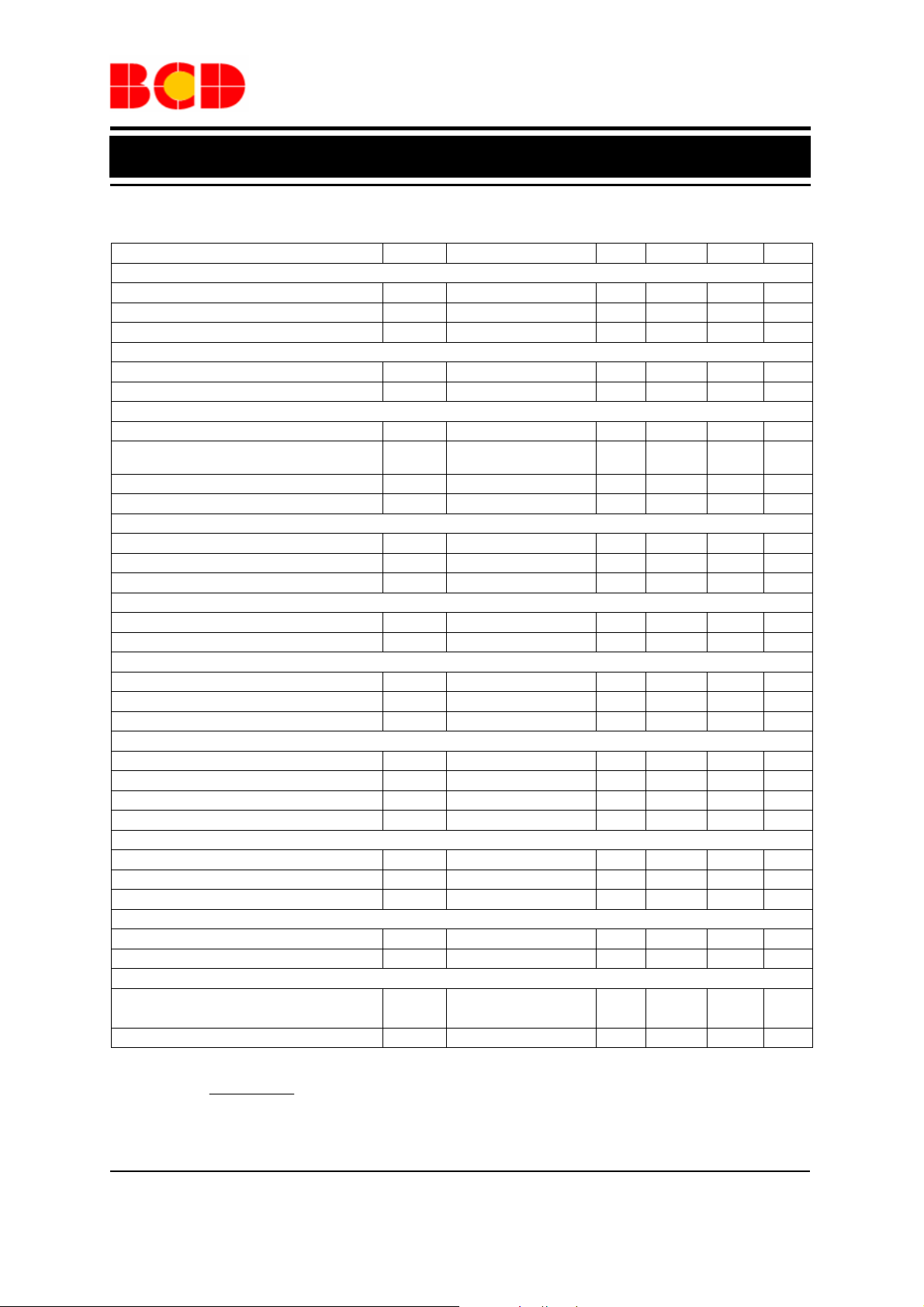
Electrical Characteristics
TA=25ºC, VIN=VEN=12V, V
Parameter Symbol Conditions Min Typ Max Unit
SUPPLY VOLTAGE (IN PIN)
Input Voltage VIN 4.5 18 V
Quiescent Current IQ VFB=1V,VEN=3V 1.2 1.4 mA
Shutdown Supply Current I
UNDER VOLTAGE LOCKOUT
Input UVLO Threshold V
Input UVLO Hysteresis V
ENABLE (EN PIN)
EN Shutdown Threshold Voltage 1.1 1.5 2 V
EN Shutdown Threshold Voltage Hysteresis
(Note 2)
EN Lockout Threshold Voltage 2.2 2.5 2.7 V
EN Lockout Hysteresis 210 mV
VOLTAGE REFERENCE (FB PIN)
Feedback Voltage VFB 0.907 0.925 0.943 V
Feedback Over Voltage Threshold V
Feedback Bias Current IFB VFB=1V -0.1 0.1
MOSFET
High-side Switch On-resistance(Note 3) R
Low-side Switch On-resistance(Note 3) R
CURRENT LIMIT
High-side Switch Leakage Current I
High-side Switch Current Limit I
Low-side Switch Current Limit I
SWITCHING REGULATOR
Oscillator Frequency f
Short Circuit Oscillator Frequency f
Max. Duty Cycle D
Min. Duty Cycle D
ERROR AMPLIFIER
Error Amplifier Voltage Gain (Note 2) AEA 400 V/V
Error Amplifier Transconductance GEA 800
COMP to Current Sense Transconductance GCS 5.2 A/V
THERMAL SHUTDOWN
Thermal Shutdown (Note 2) T
Thermal Shutdown Hysteresis (Note 2) T
SOFT START (SS PIN)
=3.3V, unless otherwise specified.
OUT
VEN=0V 0.1 10
SHDN
UVLO
VIN Rising 3.65 4.00 4.25 V
200 mV
HYS
350 mV
1.1 V
FBOV
DSONHISW
DSONLISW
LEAKH
LIMH
LIML
OSC1
OSC2
MAX
MIN
OTSD
HYS
=0.2A/0.7A
=-0.2A/-0.7A
VIN=18V,VEN=VSW=0V 0.1 10
4.3 5.6 A
From drain to Source 1.4 A
280 340 400 kHz
90 kHz
VFB=0.85V 90 %
VFB=1V 0 %
160 ºC
20 ºC
100
100
µA
µA
mΩ
mΩ
µA
A/V
Soft-start Time (Note 2) tSS
C
SS
=0.1µF
Soft-start Current VSS=0V 6
15 ms
µA
Note 2: Not tested, guaranteed by design.
V-V
Note 3: R
DSON
=
SW2SW1
.
I-I
SW2SW1
May. 2012 Rev. 1. 7 BCD Semiconductor Manufacturing Limited
5
Page 6
Data Sheet
340kHz, 3A Synchronous DC-DC Buck Converter AP3503
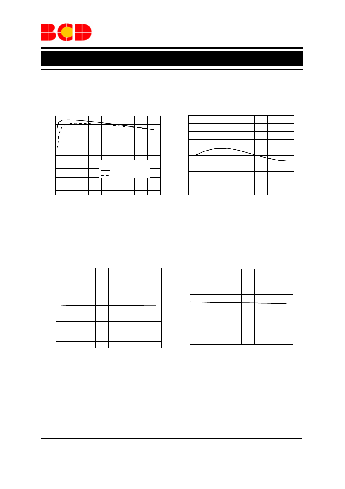
Typical Performance Characteristics
T
=25ºC, VIN=12V, V
A
=3.3V, unless otherwise noted.
OUT
100
90
80
70
60
50
Efficiency ( %)
40
30
20
10
0.0 0.4 0.8 1.2 1.6 2.0 2.4 2.8 3.2
V
=3.3V, TA=25oC, L=10µH
OUT
VIN=5V
VIN=12V
Output Current (A)
Figure 4. Efficiency vs. Output Current Figure 5. Quiescent Current vs. Case Temperature
1.2
1.1
1.0
0.9
0.8
Feedback Voltage (V)
0.7
0.6
-50 -25 0 25 50 75 100 125 150
Case Temperature (oC)
1.4
1.3
1.2
1.1
Quiescent Current (mA)
1.0
0.9
-50 -25 0 25 50 75 100 125 150
Case Temperature (oC)
3.6
3.5
3.4
3.3
3.2
Output Voltage (V)
3.1
3.0
0.0 0.4 0.8 1.2 1.6 2.0 2.4 2.8 3.2
Output Current (A)
Figure 6. Feedback Voltage vs. Case Temperature Figure 7. Output Voltag e vs. Output Current
May. 2012 Rev. 1. 7 BCD Semiconductor Manufacturing Limited
6
Page 7
Data Sheet
340kHz, 3A Synchronous DC-DC Buck Converter AP3503
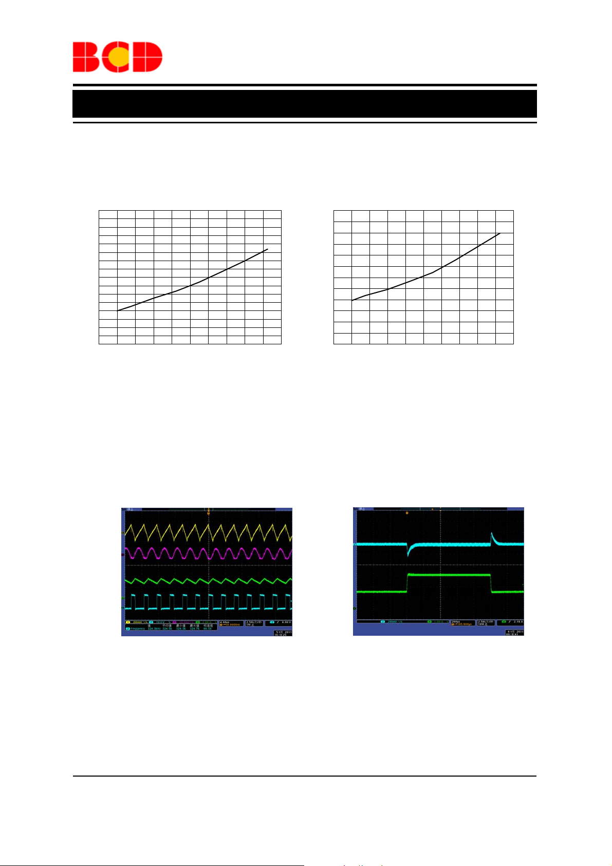
Typical Performance Characteristics (Continued)
TA=25ºC, VIN=12V, V
=3.3V, unless otherwise noted.
OUT
200
180
160
140
120
100
80
60
High-side Switch On-resistance (mΩ)
40
-60 -40 -20 0 20 40 60 80 100 120 140
Case Temperatur e (oC)
160
140
120
100
80
60
Low-side Switch On-resistance (mΩ)
40
-60 -40 -20 0 20 40 60 80 100 120 140
Case Temperature (oC)
Figure 8. High-side Switch On-resistance Figure 9. Low-side Switch On-resistance
vs. Case Temperature vs. Case Temperature
V
IN_AC
200mV/div
V
20mV/div
10V/div
OUT_AC
2A/div
VSW
IL
200mV/div
V
OUT_AC
1A/div
I
OUT
Time 4µs/div
Time 200µs/div
Figure 10. Output Ripple (I
=3A) Figure 11. Load Transient (I
OUT
=1.5A to 3A)
OUT
May. 2012 Rev. 1. 7 BCD Semiconductor Manufacturing Limited
7
Page 8
Data Sheet
340kHz, 3A Synchronous DC-DC Buck Converter AP3503
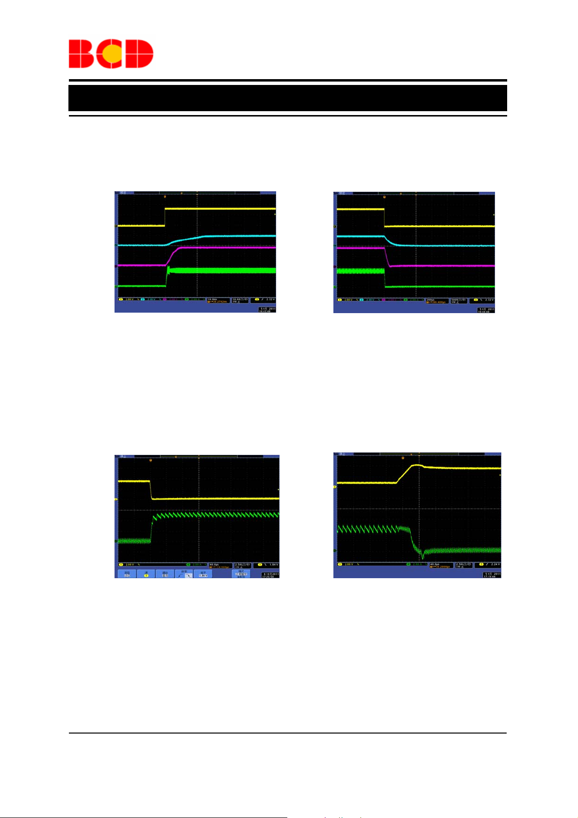
Typical Performance Characteristics (Continued)
TA=25ºC, VIN=12V, V
=3.3V, unless otherwise noted.
OUT
V
EN
2V/div
VSS
2V/div
V
OUT
2V/div
IL
2A/div
VEN
2V/div
VSS
2V/div
V
OUT
2V/div
IL
2A/div
V
OUT
2V/div
IL
2A/div
Time 10ms/div
Figure 12. Enable Turn on Characteristic Figure 13. Enable Turn off Characteristic
(VIN=12V, VEN=3.3V, V
Time 40µs/div
=3.3V, IL=3A) (VIN=12V, VEN=3.3V, V
OUT
V
OUT
2V/div
IL
2A/div
Time 200µs/div
OUT
Time 40µs/div
=3.3V, I
=3A)
L
Figure 14. Short Circuit Protection (I
=0A) Figure 15. Short Circuit Recovery (I
OUT
OUT
=0A)
May. 2012 Rev. 1. 7 BCD Semiconductor Manufacturing Limited
8
Page 9
Data Sheet
340kHz, 3A Synchronous DC-DC Buck Converter AP3503
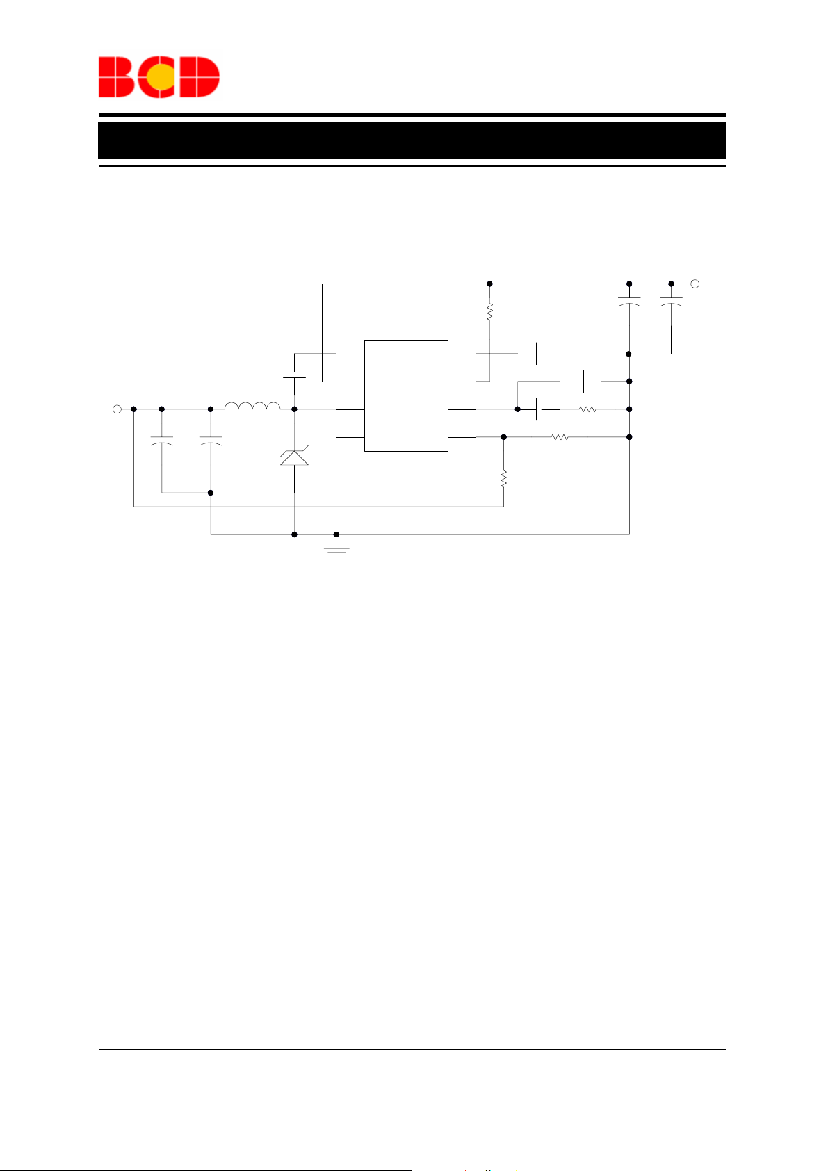
Typical Application
Input Voltage=12V
Output Voltage=3.3V
C21
22µF/25V
L 10µH
C22
22µF/25V
R4
100k
1
BS
2
C4
10nF
D1
Optional
Figure 16. Typical Application of AP3503
IN
3
SW
4
GND FB
AP3503
SS
EN
COMP
8
7
6
5
R1
26.1k
C5
0.1µF
C3
3.3nF
R2 10k
C12
10µF/25V
C6
Optional
R3
13k
C11
10µF/25V
May. 2012 Rev. 1. 7 BCD Semiconductor Manufacturing Limited
9
Page 10
Data Sheet
340kHz, 3A Synchronous DC-DC Buck Converter AP3503
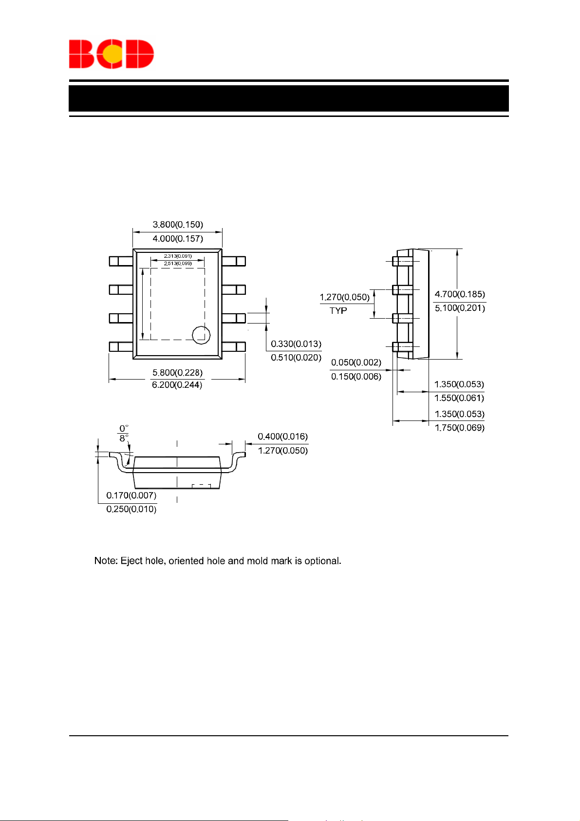
Mechanical Dimensions
PSOP-8 Unit: mm(inch)
3.202(0.126)
3.402(0.134)
May. 2012 Rev. 1. 7 BCD Semiconductor Manufacturing Limited
10
Page 11

BCD Semiconductor Manufacturing Limited
IMPORTANT NOTICE
IMPORTANT NOTICE
BCD Semiconductor Manufacturing Limited reserves the right to make changes without further notice to any products or specifi-
BCD Semiconductor Manufacturing Limited reserves the right to make changes without further notice to any products or specifi-
cations herein. BCD Semiconductor Manufacturing Limited does not assume any responsibility for use of any its products for any
cations herein. BCD Semiconductor Manufacturing Limited does not assume any responsibility for use of any its products for any
particular purpose, nor does BCD Semiconductor Manufacturing Limited assume any liability arising out of the application or use
particular purpose, nor does BCD Semiconductor Manufacturing Limited assume any liability arising out of the application or use
of any its products or circuits. BCD Semiconductor Manufacturing Limited does not convey any license under its patent rights or
of any its products or circuits. BCD Semiconductor Manufacturing Limited does not convey any license under its patent rights or
other rights nor the rights of others.
other rights nor the rights of others.
http://www.bcdsemi.com
MAIN SITE
MAIN SITE
- Headquarters
BCD Semiconductor Manufacturing Limited
BCD Semiconductor Manufactur ing Limited
- Wafer Fab
No. 1600, Zi Xing Road, Shanghai ZiZhu Science-based Industrial Park, 200241, China
Shanghai SIM-BCD Semiconductor Manufacturing Limited
Tel: +86-21-24162266, Fax: +86-21-24162277
800, Yi Shan Road, Shanghai 200233, China
Tel: +86-21-6485 1491, Fax: +86-21-5450 0008
REGIONAL SALES OFFICE
Shenzhen Office
REGIONAL SALES OFFICE
Shanghai SIM-BCD Semiconductor Manufacturing Co., Ltd., Shenzhen Office
Shenzhen Office
Unit A Room 1203, Skyworth Bldg., Gaoxin Ave.1.S., Nanshan District, Shenzhen,
Shanghai SIM-BCD Semiconductor Manufacturing Co., Ltd. Shenzhen Office
China
Advanced Analog Circuits (Shanghai) Corporation Shenzhen Office
Tel: +86-755-8826 7951
Room E, 5F, Noble Center, No.1006, 3rd Fuzhong Road, Futian District, Shenzhen 518026, China
Fax: +86-755-8826 7865
Tel: +86-755-8826 7951
Fax: +86-755-8826 7865
- Wafer Fab
BCD Semiconductor Manufacturing Limited
Shanghai SIM-BCD Semiconductor Manufacturing Co., Ltd.
- IC Design Group
800 Yi Shan Road, Shanghai 200233, China
Advanced Analog Circuits (Shanghai) Corporation
Tel: +86-21-6485 1491, Fax: +86-21-5450 0008
8F, Zone B, 900, Yi Shan Road, Shanghai 200233, China
Tel: +86-21-6495 9539, Fax: +86-21-6485 9673
Taiwan Office
BCD Semiconductor (Taiwan) Company Limited
Taiwan Office
4F, 298-1, Rui Guang Road, Nei-Hu District, Taipei,
BCD Semiconductor (Taiwan) Company Limited
Tai wan
4F, 298-1, Rui Guang Road, Nei-Hu District, Taipei,
Tel: +886-2-2656 2808
Taiwan
Fax: +886-2-2656 2806
Tel: +886-2-2656 2808
Fax: +886-2-2656 2806
USA Office
BCD Semiconductor Corp.
USA Office
30920 Huntwood Ave. Hayward,
BCD Semiconductor Corporation
CA 94544, USA
30920 Huntwood Ave. Hayward,
Tel : +1-510-324-2988
CA 94544, U.S.A
Fax: +1-510-324-2788
Tel : +1-510-324-2988
Fax: +1-510-324-2788
 Loading...