

Page 1
(
)
Green
1.5A SINGLE CHANNEL CURRENT-LIMITED
POWER SWITCH WITH OUTPUT DISCHARGE
Description
The AP2181D and AP2191D are integrated high-side power switches
optimized for Universal Serial Bus (USB) and other hot-swap
applications. The family of devices complies with USB 2.0 and is
available with both polarities of Enable input. They offer current and
thermal limiting and short circuit protection as well as controlled rise
time and under-voltage lockout functionality. A 7ms deglitch capability
on the open-drain Flag output prevents false over-current reporting
and does not require any external components.
All devices are available in SO-8, MSOP-8, MSOP-8EP, SOT25, and
U-DFN2018-6 packages.
Features
Single USB Port Power Switches with Output Discharge
Over-Current and Thermal Protection
2.1A Accurate Current Limiting
Fast Transient Response
Reverse Current Blocking
90m On-Resistance
Input Voltage Range: 2.7V – 5.5V
0.6ms Typical Rise Time
Very Low Shutdown Current: 1µA (max)
Fault Report (FLG) with Blanking Time (7ms typ)
ESD Protection: 4kV HBM, 300V MM
Active High (AP2191D) or Active Low (AP2181D) Enable
Ambient Temperature Range -40°C to +85°C
SOT25, SO-8, MSOP-8, MSOP-8EP (Exposed Pad), and
U-DFN2018-6: Available in “Green” Molding Compound
(No Br, Sb)
Lead-Free Finish; RoHS Compliant (Notes 1 & 2)
Halogen and Antimony Free. “Green” Device (Note 3)
UL Recognized, File Number E322375
IEC60950-1 CB Scheme Certified
Applications
Consumer electronics – LCD TV & Monitor, Game Machines
Communications – Set-Top-Box, GPS, Smartphone
Computing – Laptop, Desktop, Servers, Printers, Docking
Station, HUB
Notes: 1. EU Directive 2002/95/EC (RoHS) & 2011/65/EU (RoHS 2) compliant. All applicable RoHS exemptions applied.
2. See http://www.diodes.com/quality/lead_free.html for more information about Diodes Incorporated’s definitions of Halogen- and Antimony-free, "Green"
and Lead-free.
3. Halogen- and Antimony-free "Green” products are defined as those which contain <900ppm bromine, <900ppm chlorine (<1500ppm total Br + Cl) and
<1000ppm antimony compounds.
AP2181D/AP2191D
Document number: DS32251 Rev. 3 - 2
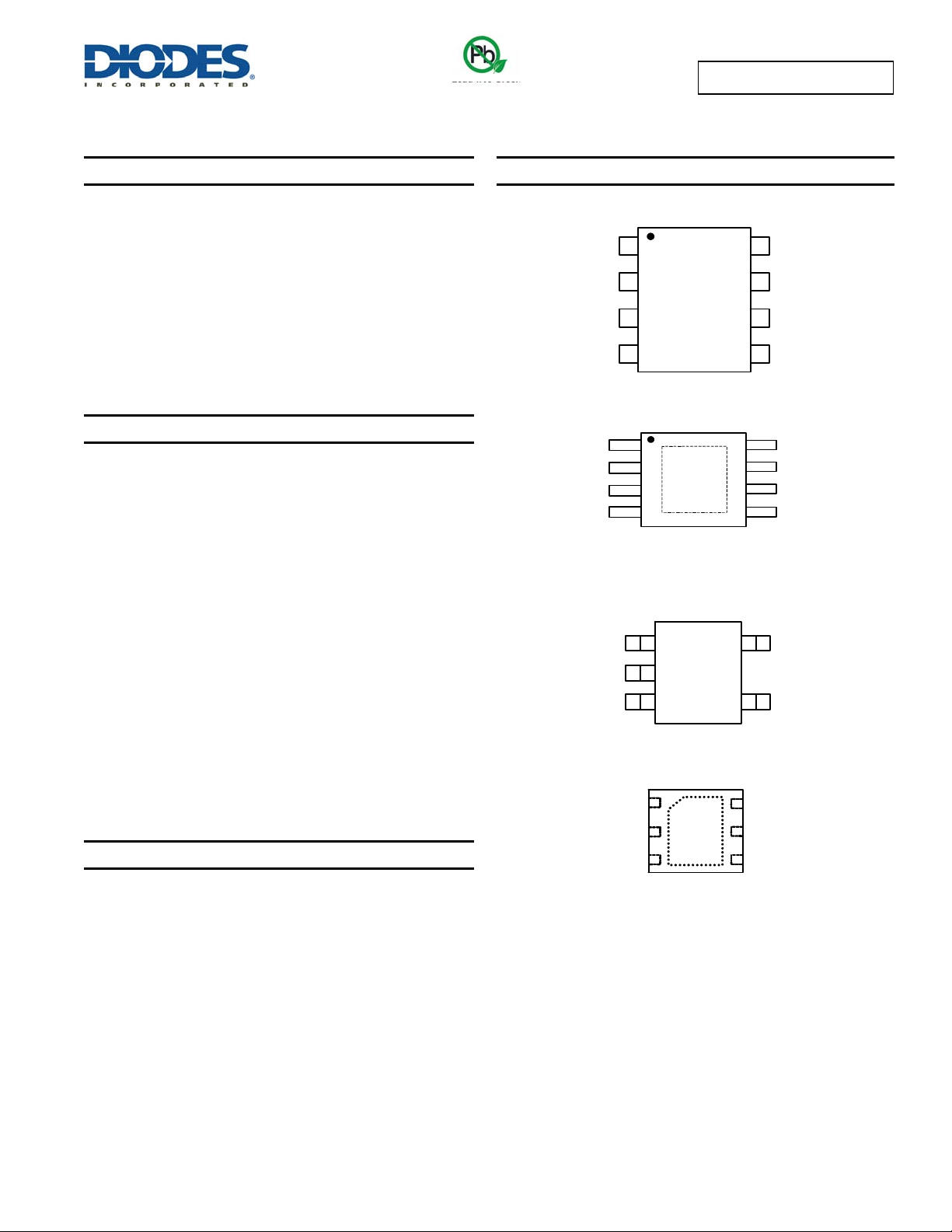
Pin Assignments
1 of 18
www.diodes.com
( Top View )
1
GND
2
IN
3
IN
4
EN
( Top View )
1
GND
2
IN
3
IN
4
EN
MSOP-8 / MSOP-8EP
Note: Latter with Exposed Pad
Dotted Line
( Top View )
OUT
GND
FLG
1
2
3
( Top View )
1
GND
2
IN
3
U-DFN2018-6
AP2181D/AP2191D
8
NC
7
OUT
6
OUT
5
FLG
SO-8
NC
8
7
OUT
6
OUT
5
FLG
5
IN
4
EN
SOT25
6
OUT
5
OUT
4
FLGEN
March 2013
© Diodes Incorporated
Page 2
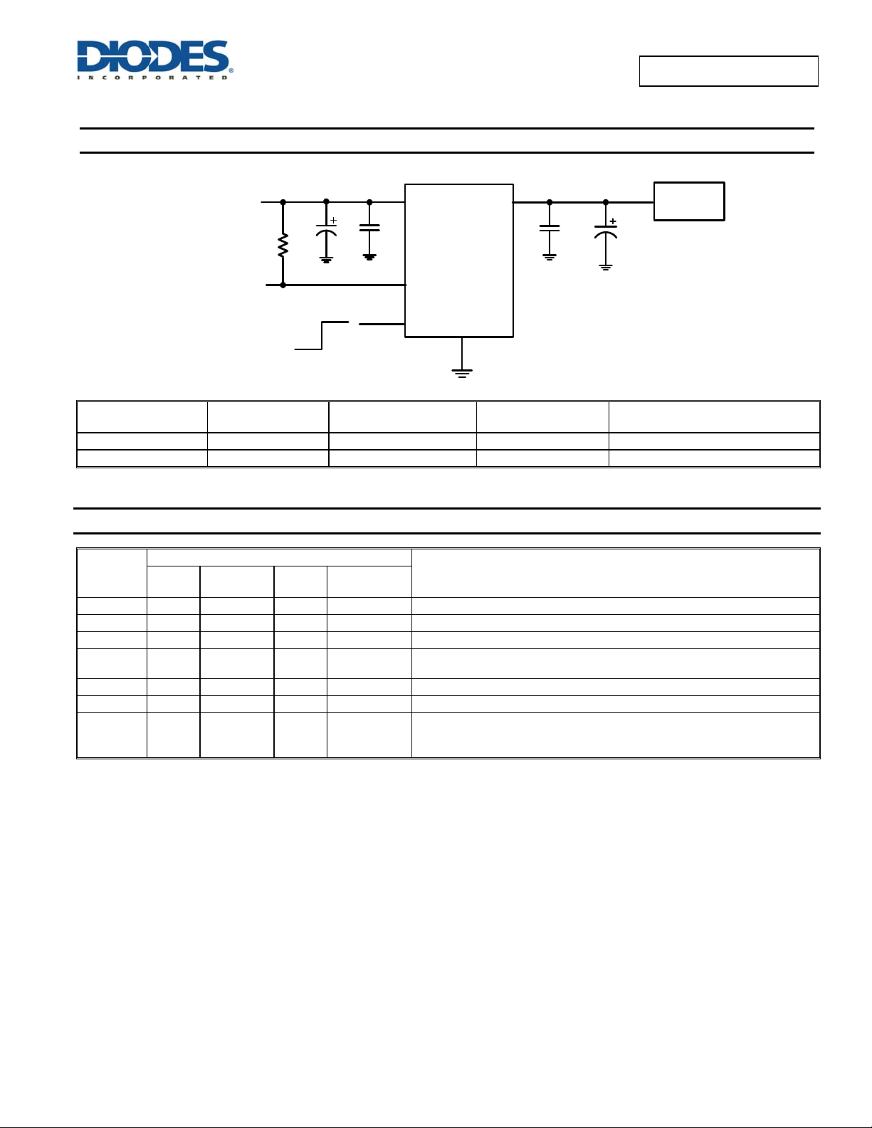
Typical Applications Circuit
AP2191D Enable Active High
Power Supply
2.7V to 5.5V
10k
10uF
0.1uF
IN
FLG
OUT
0.1uF
AP2181D/AP2191D
Load
120uF
ON
EN
GND
OFF
Available Options
Part Number Channel
AP2181D 1 Active Low 2.1A 1.5A
AP2191D 1 Active High 2.1A 1.5A
Enable Pin
(EN)
Current Limit
(Typical)
Pin Descriptions
Pin
Name
GND 1 1 2 1 Ground
IN
EN 4 4 4 3 Enable input, active low (AP2181D) or active high ( AP2191D)
FLG 5 5 3 4
OUT
NC
Exposed tab — Exposed tab — Exposed tab
SO-8
MSOP-8
2, 3 2, 3 5 2 Voltage input pin (all IN pins must be tied together externally )
6, 7 6, 7 1 5, 6 Voltage output pin (all OUT pins must be tied together externally )
8 8 N/A N/A No internal connection; recommend tie to OUT pins
AP2181D/AP2191D
Document number: DS32251 Rev. 3 - 2
Pin Number
MSOP-8EP SOT25 U-DFN2018-6
www.diodes.com
Functions
Over-current and over-temperature fault report; open-drain flag is active low w hen
triggered
Exposed pad.
It should be connected to GND and thermal mass for enhanced thermal
impedance. It shou l d n o t be u s e d as e l e c t rica l g r o u nd co n d ucti o n p a t h.
2 of 18
Recommended Maximum
Continuous Load Current
March 2013
© Diodes Incorporated
Page 3
AP2181D/AP2191D
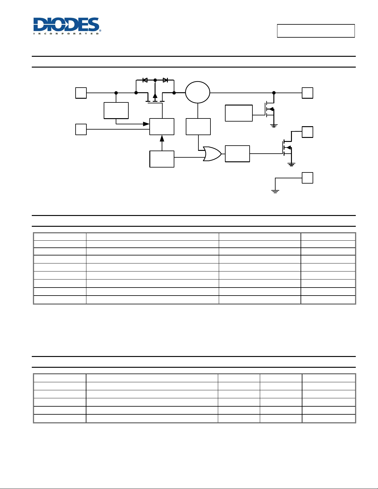
Functional Block Diagram
IN
EN
UVLO
Driver
Thermal
Sense
Current
Sense
Discharge
Control
Current
Limit
Deglitch
OUT
FLG
GND
Absolute Maximum Ratings (@T
= +25°C, unless otherwise specified.)
A
Symbol Parameter Ratings Unit
ESD HBM Human Body Model ESD Protection 4 kV
ESD MM Machine Model ESD Protection 300 V
VIN
V
OUT
V
EN , VFLG
I
LOAD
T
JMAX
TST
Caution: Stresses greater than the 'Absolute Maximum Ratings' specified above, may cause permanent damage to the device. These are stress ratings only;
Note: 4. UL Recognized Rating from -30°C to +70°C (Diodes qualified T
functional operation of the device at these or any other conditions exceeding those indicated in this specification is not implied. Device reliability may be
affected by exposure to absolute maximum rating conditions for extended periods of time.
Semiconductor devices are ESD sensitive and may be damaged by exposure to ESD events. Suitable ESD precautions should be taken when handling
and transporting these devices
Input Voltage 6.5 V
Output Voltage
VIN +0.3
Enable Voltage 6.5 V
Maximum Continuous Load Current Internal Limited A
Maximum Junction Temperature 150 °C
Storage Temperature Range (Note 4) -65 to +150 °C
from -65°C to +150°C).
ST
Recommended Operating Conditions (@T
= +25°C, unless otherwise specified.)
A
Symbol Parameter Min Max Unit
V
I
OUT
VIL
VIH
T
IN
A
Input Voltage 2.7 5.5 V
Output Current 0 1.5 A
EN Input Logic Low Voltage 0 0.8 V
EN Input Logic High Voltage 2
VIN
Operating Ambient Temperature -40 +85 °C
V
V
AP2181D/AP2191D
Document number: DS32251 Rev. 3 - 2
3 of 18
www.diodes.com
March 2013
© Diodes Incorporated
Page 4
AP2181D/AP2191D
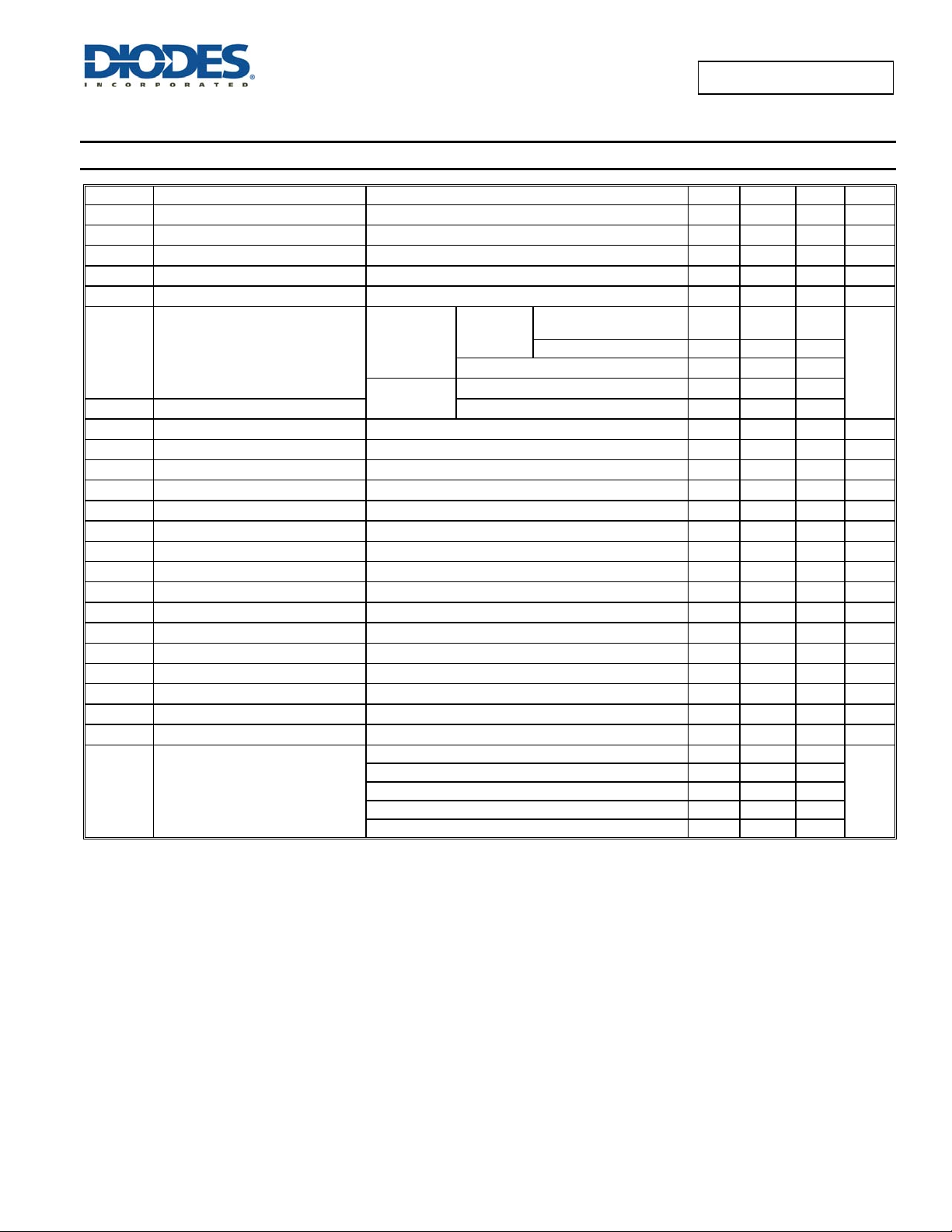
Electrical Characteristics (@T
= +25°C, VIN = +5.0V, unless otherwise specified.)
A
Symbol Parameter Test Conditions Min Typ Max Unit
V
I
SHDN
I
LEAK
I
R
DS(ON)
I
SHORT
I
LIMIT
I
I
SINK
T
D(ON)
T
D(OFF)
R
T
T
R
T
SHDN
T
Input UVLO 1.6 1.9 2.5 V
UVLO
Input Shutdown Current
Input Quiescent Current
I
Q
Disabled, I
Enabled, I
OUT
OUT
= 0
= 0
0.5 1 µA
45 70 µA
Input Leakage Current Disabled, OUT grounded 0.1 1 µA
Reverse Leakage Current
REV
Disabled, V
= 0V, V
IN
OUT
= 5V, I
REV
at VIN
SOT25, MSOP-8, SO-8,
MSOP-8-EP
U-DFN2018-6 90 110
Switch on-resistance
V
I
OUT
IN
= 5V,
= 1.5A
T
= +25°C
A
-40°C TA +85°C
VIN = 3.3V,
= 1.5A
I
Short-Circuit Current Limit
Over-Load Current Limit
Current Limiting Trigger Threshold
Trig
EN Input Logic Low Voltage
V
IL
EN Input Logic High Voltage
V
IH
EN Input leakage
Output Turn-On Delay Time
Output Turn-On Rise Time
TR
Output Turn-Off Delay Time
Output Turn-Off Fall Time
TF
FLG Output FET On-Resistance
FLG
FLG Blanking Time
Blank
Discharge Time
DIS
Discharge Resistance (Note 5)
DIS
Thermal Shutdown Threshold
Thermal Shutdown Hysteresis 25
HYS
OUT
Enabled into short circuit, CL=120µF
V
= 5V, V
IN
Output Current Slew rate (<100A/s) , CL = 120µF
= 2.7V to 5.5V
V
IN
V
= 2.7V to 5.5V
IN
= 5V
V
EN
CL = 1µF, R
CL = 1µF, R
CL = 1µF, R
CL = 1µF, R
I
=10mA
FLG
C
= 10uF, CL = 22F
IN
CL = µF, VIN = 5V, disabled to V
VIN = 5V, disabled, I
Enabled, R
T
= +25°C
A
OUT
+85°C
A
= 1mA
OUT
< 0.5V
-40°C T
= 4V, CL = 120µF, -40°C TA +85°C
OUT
= 10
LOAD
= 10
LOAD
= 10
LOAD
= 10
LOAD
= 1k
LOAD
0.1 1 µA
95 115
140
120 140
170
2.0 A
1.6 2.1 2.6 A
2.6 A
0.8 V
2 V
1 µA
0.05 ms
0.6 1.5 ms
0.05 ms
0.05 0.1 ms
20 40
4 7 15 ms
0.6 ms
100
140
m
C
C
SOT25 (Note 6) 170
Thermal Resistance Junction-to-
JA
Ambient
SO-8 (Note 6) 127
MSOP-8 (Note 6) 118
MSOP-8-EP (Note 7) 67
o
C/W
U-DFN2018-6 (Note 7) 70
Notes: 5. The discharge function is active when the device is disabled (when enable is de-asserted). The discharge function offers a resistive discharge path
for the external storage capacitor.
6. Device mounted on FR-4 substrate PCB, 2oz copper, with minimum recommended pad layout.
7. Device mounted on 2” x 2” FR-4 substrate PCB, 2oz copper, with minimum recommended pad on top layer and thermal vias to bottom layer ground
plane.
AP2181D/AP2191D
Document number: DS32251 Rev. 3 - 2
4 of 18
www.diodes.com
March 2013
© Diodes Incorporated
Page 5
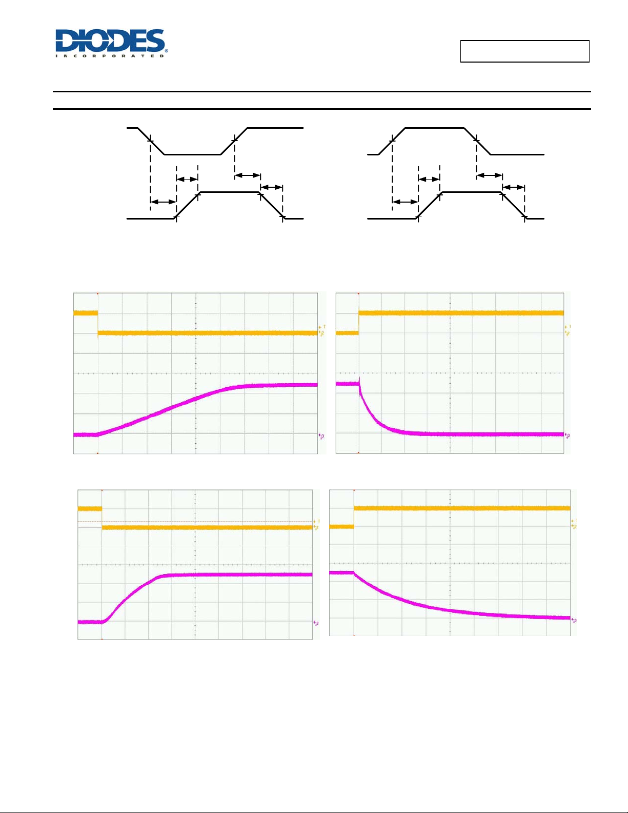
Typical Performance Characteristics
AP2181D/AP2191D
Ven
5V/div
Vout
2V/div
Ven
5V/div
V
EN
V
OUT
50%
T
D(ON)
T
10%
50%
T
R
90%
D(OFF)
90%
10%
T
F
V
EN
50%
T
T
D(ON)
V
OUT
10%
50%
T
R
90%
D(OFF)
90%
10%
T
F
Figure 1 Voltage Waveforms: AP2181D (left), AP2191D (right)
All Enable Plots are for AP2181D Active Low
Turn-On Delay and Rise Time
CL = 1µF
TA = +25°C
RL = 10
Ven
5V/div
Vout
2V/div
Turn-Off Delay and Fall Time
CL = 1µF
TA = +25°C
RL = 10
100µs/div
Turn-On Delay and Rise Time
Ven
5V/div
100µs/div
Turn-Off Delay and Fall Time
Vout
2V/div
AP2181D/AP2191D
Document number: DS32251 Rev. 3 - 2
500µs/div
CL = 120µF
TA = +25°C
RL = 10
www.diodes.com
5 of 18
Vout
2V/div
500µs/div
CL = 120µF
TA = 25°C
RL = 10
March 2013
© Diodes Incorporated
Page 6
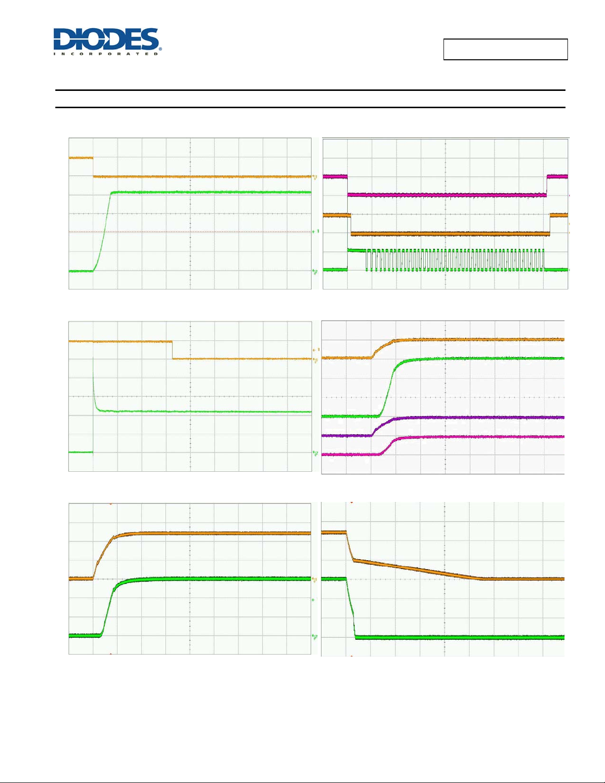
Typical Performance Characteristics (cont.)
Iout
500mA/div
Short Circuit Current, Device Enabled Into Short
Ven
5V/div
V
= 5V
IN
TA = +25°C
CL = 120µF
AP2181D/AP2191D
Short Circuit with Blanking Time and Recovery
Vout
5V/div
Vflag
5V/div
Iout
2A/div
V
= 5V
IN
TA = +25°C
CL = 120µF
Vflag
2V/div
Iout
1A/div
Vin
2V/div
500us/div
0.6 Ω Load Connected to Enabled Device
2ms/div
UVLO Increasing With Full Load
V
= 5V
IN
TA = +25°C
CL = 120µF
Vin
5V/div
Iout
500mA/div
Vflg
5V/div
Vout
5V/div
Vin
2V/div
50ms/div
Power On with Full Load
1ms/div
UVLO Decreasing With Full Load
TA = +25°C
CL = 120µF
RL = 3.3
TA = +25°C
CL = 22µF
RL = 3.3
Iout
500mA/div
AP2181D/AP2191D
Document number: DS32251 Rev. 3 - 2
1ms/div
TA = +25°C
CL = 22µF
RL = 3.3
www.diodes.com
6 of 18
Iout
500mA/div
10ms/div
March 2013
© Diodes Incorporated
Page 7
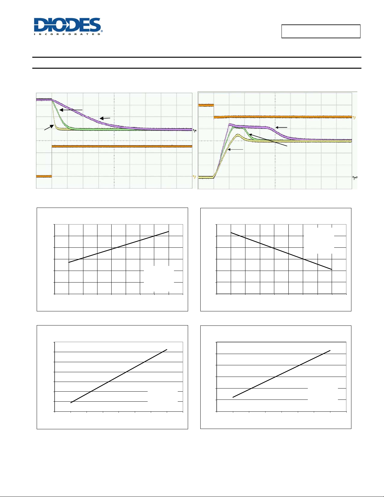
Typical Performance Characteristics (cont.)
Discharge Time
(No Load Resistance)
Vout
2V/div
=22µF
C
L
Ven
2V/div
850
750
650
CL =120µF
C
=470µF
L
100ms/div
Turn-On Time vs Input Voltage
TA = +25°C
V
= 5V
IN
No Load
Resistance
Ven
5V/div
Iout
500mA/div
55
50
45
AP2181D/AP2191D
Inrush Current
CL=470uF
CL=220uF CL=100uF
1ms/div
Turn-O f f Time vs I nput Vol tage
V
TA = +25°C
RL = 3.3
CL = 1µF
RL = 10
TA = +25°C
IN
= 5V
550
450
Turn-On Time (us)
350
250
1.522.533.544.555.56
Input V o ltage (V)
CL = 1µF
RL = 10
TA = +25°C
Rise Time vs I nput Vol t age
650
600
550
500
450
Rise Time (us)
400
350
300
22.533.544.555.56
Input V o ltage (V)
CL = 1µF
RL = 10
T
= +25°C
A
40
35
Turn-Off Time (us)
30
25
1.5 2 2.5 3 3.5 4 4.5 5 5.5 6
Input Voltage (V)
Fall Time vs Input Voltage
25
24
23
22
Fall Time (us )
21
20
19
22.533.544.555.56
Input Voltage (V)
CL = 1µF
RL = 10
TA = +25°C
AP2181D/AP2191D
Document number: DS32251 Rev. 3 - 2
7 of 18
www.diodes.com
March 2013
© Diodes Incorporated
Page 8
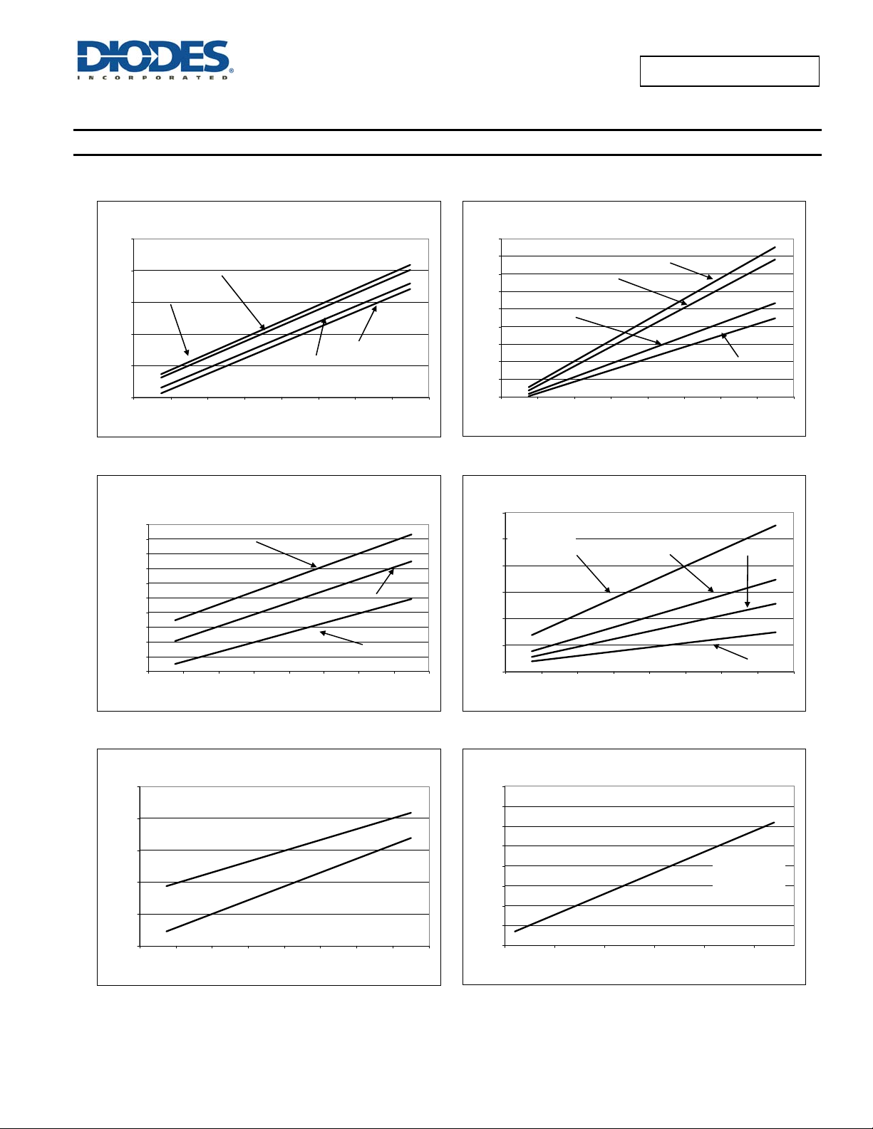
Typical Performance Characteristics (cont.)
Supply Current , Output Enabled vs Am bient Tem per at ur e
52
47
Vin =
42
37
32
Supply Current, Output Enab led (uA)
27
5.5V
-60 -40 -20 0 20 40 60 80 100
Vin = 5.0V
Vin = 2.7V
Vin = 3.3V
Ambient Temperature (°C)
AP2181D/AP2191D
Supply Current, Out put Di sabled vs A m bi ent Temperat ur e
0.9
0.8
0.7
0.6
0.5
0.4
0.3
0.2
0.1
Supply Current, Output Disable d (uA)
0.0
-60 -40 -20 0 20 40 60 80 100
Vin = 3.3V
Vin = 5.0V
Ambient Tem peratu re (°C )
Vin = 5.5V
Vin = 2.7V
Static Drain- Source On- Stat e Resist ance vs A m bient
180
170
160
150
140
130
120
110
Resistance (mΩ)
100
Static Drain-Source On-State
90
80
-60 -40 -20 0 20 40 60 80 100
Temperature
Vin = 2.7V
Vin = 3.3V
Vin = 5V
Ambient Temperature (°C)
Undervoltage Lockout vs Am bi ent Tem perat ur e
2.15
2.10
2.05
2.00
1.95
Undervoltage Lockout (V)
1.90
-60 -40 -20 0 20 40 60 80 100
UVLO Rising
UVLO Falling
Amb ient Temperature (°C)
Short- Circui t Out put Cur r e nt v s Ambi en t Te m pe r ature
2.60
CL = 100µF
2.50
2.40
2.30
2.20
2.10
Short-Circuit Output Current (A)
2.00
-60 -40 -20 0 20 40 60 80 100
3.24
3.22
3.20
3.18
3.16
3.14
3.12
Threshold Trip Current (A)
3.10
3.08
2.83.33.84.34.85.3
Vin = 2.7V
Ambient Temperature (°C)
Threshold Tri p Curr ent vs Input Volta ge
Vin = 3.3V
Input Voltage (V)
Vin = 5.0V
TA = +25°C
CL = 120µF
Vin = 5.5V
AP2181D/AP2191D
Document number: DS32251 Rev. 3 - 2
8 of 18
www.diodes.com
March 2013
© Diodes Incorporated
Page 9
AP2181D/AP2191D
Application Note
The AP2181D and AP2191D are integrated high-side power switches optimized for Universal Serial Bus (USB) that require protection functions.
The power switches are equipped with a driver that controls the gate voltage and incorporates slew-rate limitation. This, along with the various
protection features and special functions, makes these power switches ideal for hot-swap or hot-plug applications.
Protection Features:
Under-Voltage Lockout (UVLO)
Under-voltage lockout function (UVLO) guarantees that the internal power switch is initially off during start-up. The UVLO functions only when the
switch is enabled. Even if the switch is enabled, the switch is not turned ON until the power supply has reached at leas t 1.9V. Whe never the inpu t
voltage falls below approximately 1.9V, the power switch is turned off. This facilitates the design of hot-insertion systems where it is not possible
to turn off the power switch before input power is removed.
Over-Current and Short Circuit Protection
An internal sensing FET is employed to check for over-current conditions. Unlike current-sense resistors, sense FETs do not increase the series
resistance of the current path. When an overcurrent condition is detected, the device maintains a constant output cur rent and reduces the output
voltage accordingly. Complete shutdown occurs only if the fault stays long enough to activate thermal limiting.
The different overload conditions and the corresponding response of the AP2181D/AP2191D are outlined below:
S. NO Conditions Explanation Behavior of the AP2181D/AP2191D
1 Short circuit condition at start-up
Short-circuit or over current
2
condition
Gradual increase from nominal
3
operating current to I
Note that when the output has been shorted to GND at extreme ly low temperature (< -20°C), a minimum 120-F electrolytic capacitor on the
output pin is recommended. A correct capacitor type with capacitor voltage rating and temperature characteristics must be properl y chosen so
that capacitance value does not drop too low at the extremely low temperature operation. A recommended capacitor should have temperature
characteristics of less than 10% variation of capacitance change when operated at extremely low temp. Our recommended aluminum electrolytic
capacitor type is Panasonic FC series.
LIMIT
Output is shorted before
input voltage is applied or
before the part is enabled.
Short-circuit or overload
condition that occurs when
the part is enabled.
Load increases gradually
until the current-limit
threshold.(I
TRIG
)
The IC senses the short circuit and immediately clamps
output current to a certain safe level namely I
At the instance the overload occurs, higher current may flow
for a very short period of time before the current limit
function can react.
After the current limit function has tripped (reached the
over-current trip threshold), the device switches into current
limiting mode and the current is clamped at I
The current rises until I
threshold has been reached, the device switches into its
current limiting mode and is set at I
or thermal limit. Once the
TRIG
.
LIMIT
LIMIT.
LIMIT
.
Thermal Protection
Thermal protection prevents the IC from damage when the die temperature exceeds safe margins. This mainly occurs when heavy-overload or
short-circuit faults are present for extended periods of time. The AP2181D/AP2191D implements thermal sensing to monitor the operating junction
temperature of the power distribution switch. Once the die temperature rises to approximately +140°C, the Thermal protection feature gets
activated as follows: The internal thermal sense circuitry turns the power switch off and the FLG output is asserted thus preventing the power
switch from damage. Hysteresis in the thermal sense circuit allows the device to cool down to approximately +25°C before the output is turned
back on. The built-in thermal hysteresis feature avoids undesirable oscillations of the thermal protection circuit. The switch continues to cycle in
this manner until the load fault is removed, resulting in a pulsed output. The FLG open-drain output is asserted when an over-current occ urs with
7-ms deglitch.
Reverse Current Protection
In a normal MOSFET switch, current can flow in reverse direction (from the output side to the input side) when the output side voltage is higher
than the input side, even when the switch is turned off. A reverse-current blocking feature is implemented in the AP21x1 series to prevent such
back currents. This circuit is activated by the difference between the output voltage and the input voltage. When the switch is disabled, this feature
blocks reverse current flow from the output back to the input.
AP2181D/AP2191D
Document number: DS32251 Rev. 3 - 2
9 of 18
www.diodes.com
March 2013
© Diodes Incorporated
Page 10

AP2181D/AP2191D
Application Note (cont.)
Special Functions:
Discharge Function
When enable is de-asserted, the discharge function is active. The output capacitor is discharged through an internal NMOS that has a discharge
resistance of 100. Hence, the output voltage drops down to zero. The time taken for discharge is dependent on the RC time constant of the
resistance and the output capacitor.
FLG Response
The FLG open-drain output goes active low for any of the two conditions: Over-Current or Over-Temperature. The time from when a fault
condition is encountered to when the FLG output goes low is 7-ms (TYP). The FLG output remains low until both over-current and overtemperature conditions are removed. Connecting a heavy capacitive load to the output of the device can cause a momentary Over-current
condition, which does not trigger the FLG due to the 7-ms deglitch timeout. This 7-ms timeout is also applicable for Over-current recovery and
Thermal recovery. The AP2181D/AP2191D is designed to eliminate erroneous Over-current reporting without the need for external components,
such as an RC delay network.
Power Supply Considerations
A 0.01-F to 0.1-F X7R or X5R ceramic bypass capacitor between IN and GND, close to the device, is recommended. This limits the input
voltage drop during line transients. Placing a high-value electrolytic capacitor on the input (10-F minimum) and output pin(s) is recommended
when the output load is heavy. This precaution also reduces power-supply transients that may cause ringing on the input. Additionall y, bypassing
the output with a 0.01-F to 0.1-F ceramic capacitor improves the immunity of the device to short-circuit transients. This capacitor also prevents
output from going negative during turn-off due to inductive parasitics.
Power Dissipation and Junction Temperature
The low on-resistance of the internal MOSFET allows the small surface-mount packages to pass large current. Using the maximum operating
ambient temperature (T
= R
P
D
The junction temperature can be calculated by:
Where:
DS(ON)
= PD x R
T
J
T
= Ambient temperature °C
A
R
= Thermal resistance
JA
= Total power dissipation
P
D
Generic Hot-Plug Applications
In many applications it may be necessary to remove modules or PC boards while the main unit is still operating. These are considered hot-plug
applications. Such implementations require the control of current surges as seen by the main power supply and the card being inserted. The most
effective way to control these surges is to limit and slowly ramp up the current and voltage being applied to the card, similar to the way in which a
power supply normally turns on. Due to the controlled rise and fall times of the AP2181D/AP2191D, these devices can be used to provide a softer
start-up to devices being hot-plugged into a powered system. The UVLO feature of the AP2181D/AP2191D also ensures that the switch is off after
the card has been removed, and that the switch is off during the next insertion.
By placing the AP2181D/AP2191D between the V
The typical rise time of the switch is approximately 1ms, providing a slow voltage ramp at the output of the device. This implementation controls
the system surge current and provides a hot-plugging mechanism for any device.
JA
× I2
+ TA
) and R
A
, the power dissipation can be calculated by:
DS(ON)
input and the rest of the circuitry, the input power reaches these devices first after insertion.
CC
AP2181D/AP2191D
Document number: DS32251 Rev. 3 - 2
10 of 18
www.diodes.com
March 2013
© Diodes Incorporated
Page 11
g
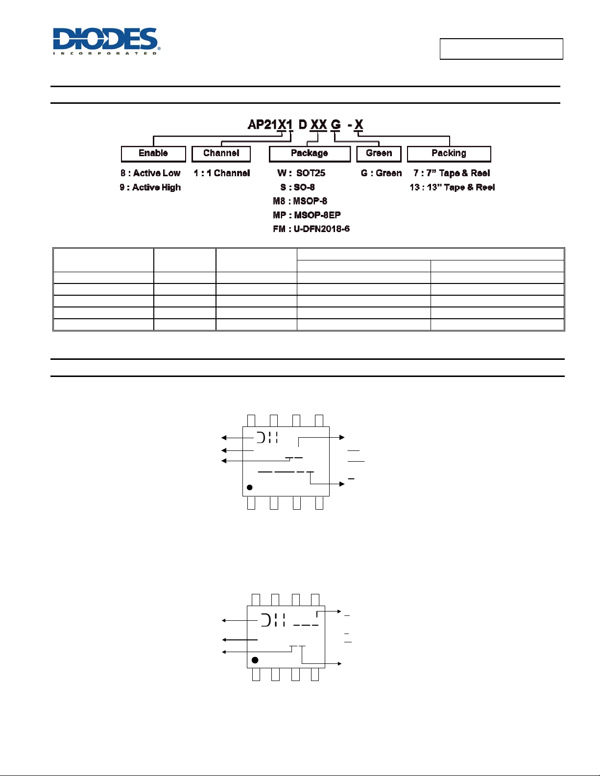
Ordering Information
AP2181D/AP2191D
Part Number Package Code Packaging
AP21X1DSG-13 S SO-8 2500/Tape & Reel -13
AP21X1DM8G-13 M8 MSOP-8 2500/Tape & Reel -13
AP21X1DMPG-13 MP MSOP-8EP 2500/Tape & Reel -13
AP21X1DWG-7 W SOT25 3000/Tape & Reel -7
AP21X1DFMG-7 FM U-DFN2018-6 3000/Tape & Reel -7
Quantity Part Number Suffix
7”/13” Tape and Reel
Marking Information
(1) SO-8
(2) MSOP-8
Logo
Part Number
6 : Active Low
8 : Active Low
7 : Active High
9 : Active Hi
h
( Top View )
8765
AP21X X D
YY WW X X
2
1
34
1 : 1 Channel
: Year : 08, 09,10~
YY
WW
: Week : 01~52; 52
represents 52 and 53 week
: Internal Code
X
G : Green
AP2181D/AP2191D
Document number: DS32251 Rev. 3 - 2
Logo
Logo
Part Number
Part Number
8 : Active Low
0 : Active Low
9 : Active High
1 : Active High
( Top view )
8765
Y
W X
AP21 X 1 D
AP23 X 1
234
1
11 of 18
www.diodes.com
A~Z : Green
X: Inte rn a l Co d e
Y
: Year : 0~9
: Year : 0~9
Y
: Week : A~Z : 1~26 week;
W
W
: Week : A~Z : 1~26 week;
a~z : 27~52 week; z represents
a~z : 27~52 week; z represents
52 and 53 week
52 and 53 week
1 : 1 Channel
1 : 1 Channel
March 2013
© Diodes Incorporated
Page 12
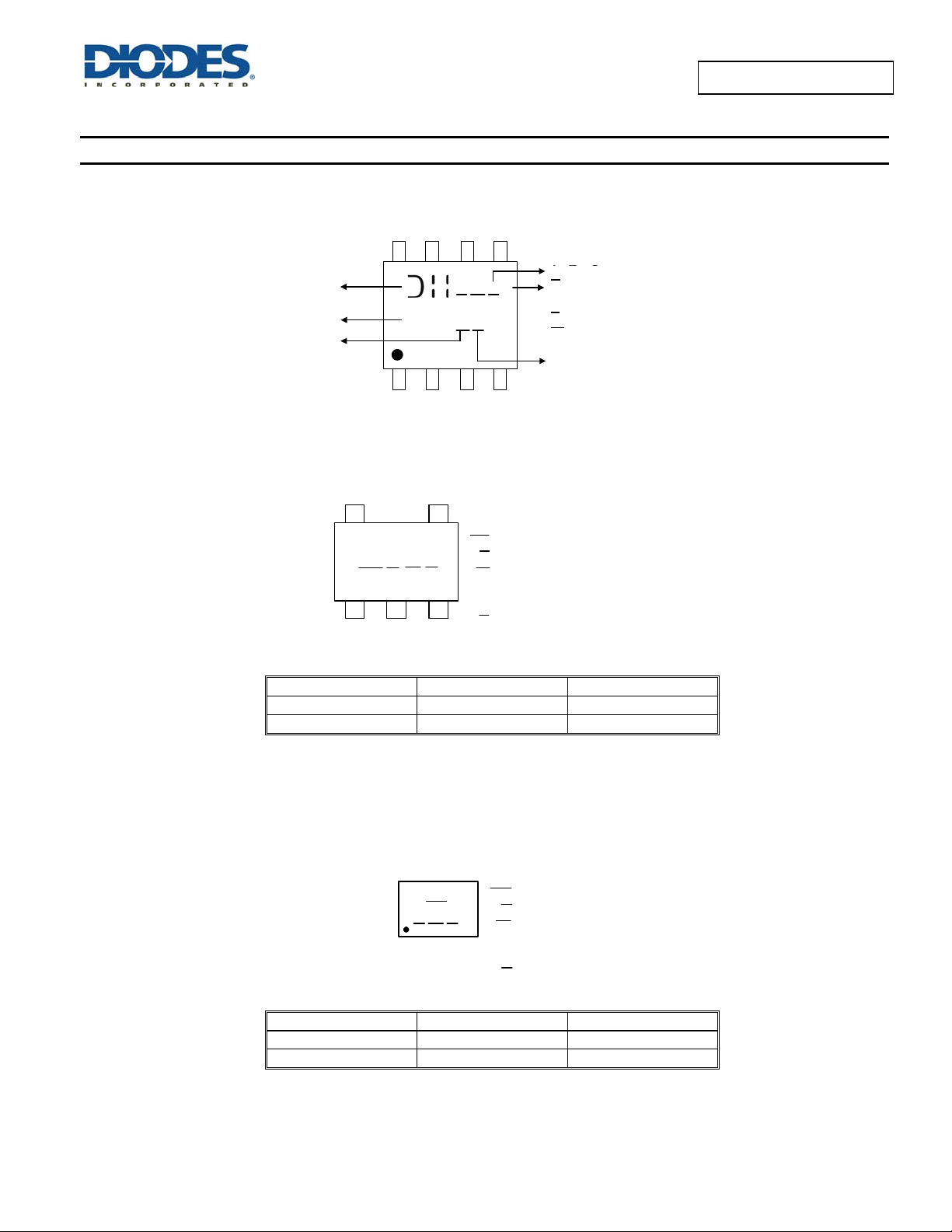
Marking Information (cont.)
(3) MSOP-8EP
Part Number
Part Number
8 : Active Low
0 : Active Low
9 : Active High
1 : Active High
(4) SOT25
Logo
Logo
( Top view )
8765
AP21 X 1 D
AP23 X 1
234
1
( Top View )
W X E
Y
AP2181D/AP2191D
A~Z : Green
X: Inte r n a l C o d e
MSOP-8-EP
MSOP-8EP
: Year : 0~9
Y
Y
: Year : 0~9
W
: Week : A~Z : 1~26 week;
W
: Week : A~Z : 1~26 week;
a~z : 27~52 week; z represents
a~z: 27~52 week; z repre sents
52 and 53 week
52 and 53 week
1 : 1 Channel
1 : 1 Channel
(5) U-DFN2018-6
AP2181D/AP2191D
Document number: DS32251 Rev. 3 - 2
W X
7
4
XX : Identification code
Y
: Year 0~9
: Week : A~Z : 1~26 week;
W
a~z : 27~52 week; z represents
52 and 53 week
: A~Z : Green
X
5
Y
XX
1 2 3
Device Package Type Identification Code
AP2181DW SOT25 JE
AP2191DW SOT25 JF
(Top View)
XX
XX
W X
Y
Device Package Type Identification Code
AP2181DFM U-DFN2018-6 JE
AP2191DFM U-DFN2018-6 JF
www.diodes.com
: Identification Code
Y : Year : 0~9
: Week : A~Z : 1~26 week;
W
a~z : 27~52 week; z represents
52 and 53 week
X
: A~Z : Green
12 of 18
© Diodes Incorporated
March 2013
Page 13
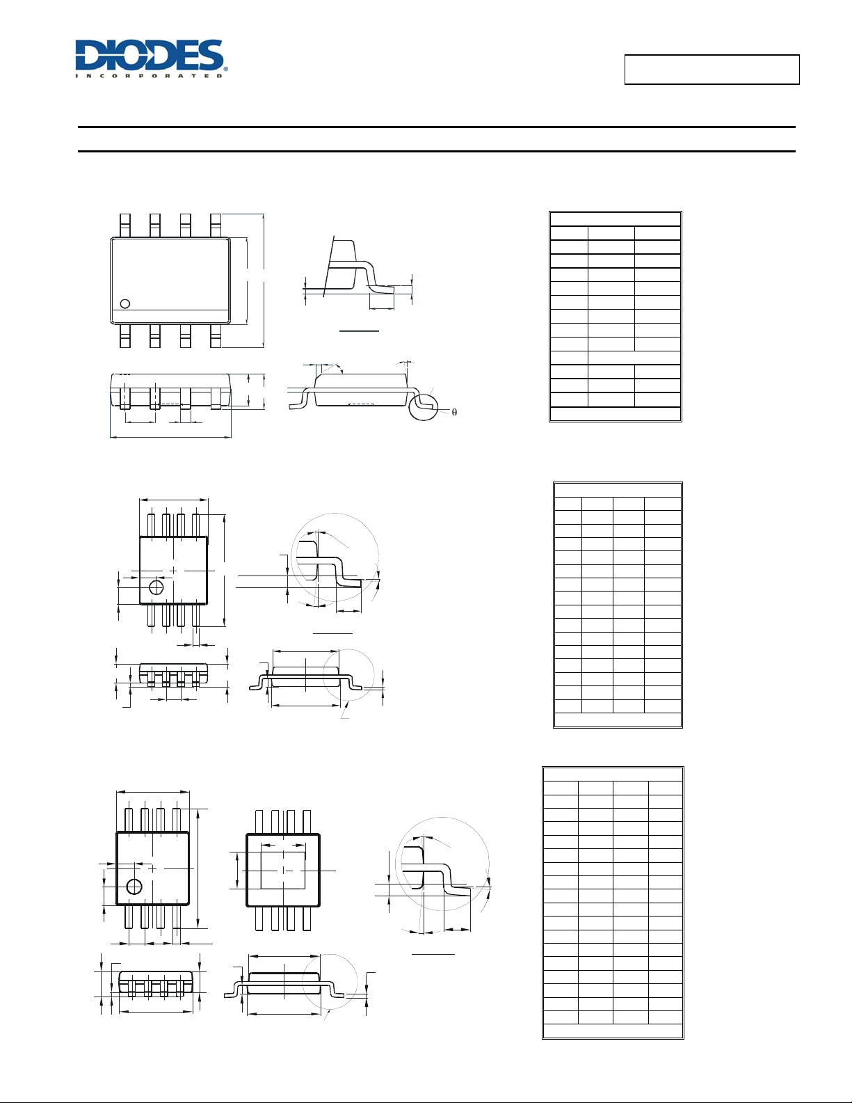
Package Outline Dimensions (All dimensions in mm.)
Please see AP02002 at http://www.diodes.com/datasheets/ap02002.pdf for latest version.
(1) SO-8
e
(2) MSOP-8
b
D
D
E1
A2
E
A1
Detail ‘A’
h
°
45
A3
A
L
0.254
Gaug e Plane
Seating Plane
7°~9
°
Detail ‘A’
x
y
1
A2
A1
(3) MSOP-8EP
D
0.25
E
Gauge Plane
Seating Plane
b
A3
A
e
4
x
1
Detail C
E3
E1
0
°
4
x
1
0
°
L
See Detail C
a
c
AP2181D/AP2191D
Document number: DS32251 Rev. 3 - 2
x
y
1
e
A1
A
D
E
8Xb
A2
E2
A3
D1
E3
E1
Gauge Plane
Seating Plane
c
See Detail C
0.25
4
X
1
4
X
1
0
°
0
°
L
Detail C
13 of 18
www.diodes.com
a
AP2181D/AP2191D
Dim Min Max
Dim Min Max Typ
All Dimensions in mm
Dim Min Max Typ
A - 1.10 A1 0.05 0.15 0.10
A2 0.75 0.95 0.86
A3 0.29 0.49 0.39
b 0.22 0.38 0.30
c 0.08 0.23 0.15
D 2.90 3.10 3.00
D1 1.60 2.00 1.80
E 4.70 5.10 4.90
E1 2.90 3.10 3.00
E2 1.30 1.70 1.50
E3 2.85 3.05 2.95
e - - 0.65
L 0.40 0.80 0.60
a 0° 8° 4°
x - - 0.750
y - - 0.750
All Dimensions in mm
SO-8
A - 1.75
A1 0.10 0.20
A2 1.30 1.50
A3 0.15 0.25
b 0.3 0.5
D 4.85 4.95
E 5.90 6.10
E1 3.85 3.95
e 1.27 Typ
h - 0.35
L 0.62 0.82
0 8
All Dimensions in mm
MSOP-8
A - 1.10 A1 0.05 0.15 0.10
A2 0.75 0.95 0.86
A3 0.29 0.49 0.39
b 0.22 0.38 0.30
c 0.08 0.23 0.15
D 2.90 3.10 3.00
E 4.70 5.10 4.90
E1 2.90 3.10 3.00
E3 2.85 3.05 2.95
e - - 0.65
L 0.40 0.80 0.60
a 0° 8° 4°
x - - 0.750
y - - 0.750
MSOP-8EP
March 2013
© Diodes Incorporated
Page 14
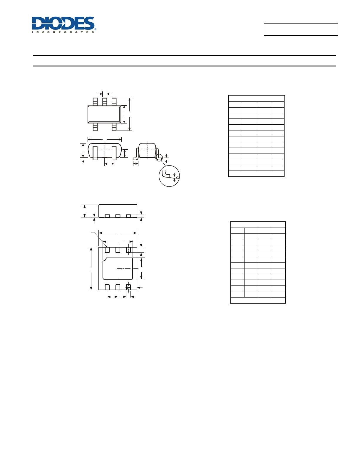
Package Outline Dimensions (cont.) (All dimensions in mm.)
Please see AP02002 at http://www.diodes.com/datasheets/ap02002.pdf for latest version.
(4) SOT25
A
B C
K
J
H
N
D
L
M
(5) U-DFN2018-6
A
A1
Pin#1 ID
E
AP2181D/AP2191D
Document number: DS32251 Rev. 3 - 2
D
D2
e
A3
SEATING PLANE
L
E2
z
b
14 of 18
www.diodes.com
AP2181D/AP2191D
Dim Min Max Typ
SOT25
A 0.35 0.50 0.38
B 1.50 1.70 1.60
C 2.70 3.00 2.80
D
H 2.90 3.10 3.00
J 0.013 0.10 0.05
K 1.00 1.30 1.10
L 0.35 0.55 0.40
M 0.10 0.20 0.15
N 0.70 0.80 0.75
0° 8°
All Dimensions in mm
U-DFN2018-6
Dim Min Max Typ
A 0.545 0.605 0.575
A1 0 0.05 0.02
A3
b 0.15 0.25 0.20
D 1.750 1.875 1.80
D2 1.30 1.50 1.40
e
E 1.95 2.075 2.00
E2 0.90 1.10 1.00
L 0.20 0.30 0.25
z
All Dimensions in mm
0.95
0.13
0.50
0.30
March 2013
© Diodes Incorporated
Page 15
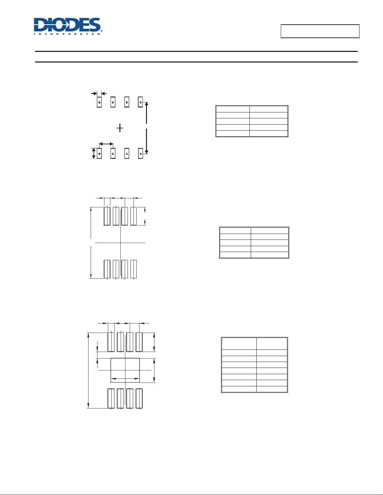
Suggested Pad Layout
Please see AP02001 at http://www.diodes.com/datasheets/ap02001.pdf for the latest version.
(1) SO-8
X
C2
Y
(2) MSOP-8
X C
Y1
(3) MSOP-8-EP
AP2181D/AP2191D
Document number: DS32251 Rev. 3 - 2
G
Y2
C1
Y
X C
Y
Y1
X1
15 of 18
www.diodes.com
Dimensions Value (in mm)
X 0.60
Y 1.55
C1 5.4
C2 1.27
Dimensions Value (in mm)
C 0.650
X 0.450
Y 1.350
Y1 5.300
Dimensions
C 0.650
G 0.450
X 0.450
X1 2.000
Y 1.350
Y1 1.700
Y2 5.300
Value
(in mm)
AP2181D/AP2191D
March 2013
© Diodes Incorporated
Page 16
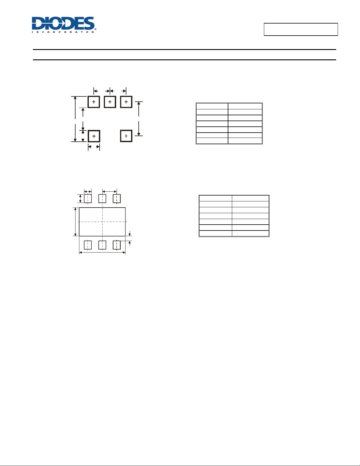
Suggested Pad Layout (cont.)
Please see AP02001 at http://www.diodes.com/datasheets/ap02001.pdf for the latest version.
(4) SOT25
C2C2
G
Z
C1
Y
X
Dimensions Value (in mm)
Z
G
X
Y
C1 2.40
C2
(5) U-DFN2018-6
AP2181D/AP2191D
Document number: DS32251 Rev. 3 - 2
XC
Y
Y1
Dimensions Value (in mm)
C 0.50
G 0.20
X 0.25
X1 1.60
Y 0.35
Y1 1.20
G
X1
16 of 18
www.diodes.com
3.20
1.60
0.55
0.80
0.95
AP2181D/AP2191D
March 2013
© Diodes Incorporated
Page 17
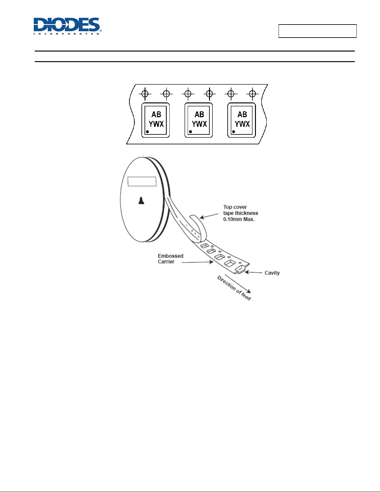
Taping Orientation (Note 8)
For U-DFN2018-6
AP2181D/AP2191D
Note: 8. The taping orientation of the other package type can be found on our website at http://www.diodes.com/datasheets/ap02007.pdf
AP2181D/AP2191D
Document number: DS32251 Rev. 3 - 2
17 of 18
www.diodes.com
March 2013
© Diodes Incorporated
Page 18

AP2181D/AP2191D
DIODES INCORPORATED MAKES NO WARRANTY OF ANY KIND, EXPRESS OR IMPLIED, WITH REGARDS TO THIS DOCUMENT,
INCLUDING, BUT NOT LIMITED TO, THE IMPLIED WARRANTIES OF MERCHANTABILITY AND FITNESS FOR A PARTICULAR PURPOSE
(AND THEIR EQUIVALENTS UNDER THE LAWS OF ANY JURISDICTION).
Diodes Incorporated and its subsidiaries reserve the right to make modifications, enhancements, improvements, corrections or other changes
without further notice to this document and any product described herein. Diodes Incorporated does not assume any liability arising out of the
application or use of this document or any product described herein; neither does Diodes Incorporated convey any license under its patent or
trademark rights, nor the rights of others. Any Customer or user of this document or products described herein in such applications shall assume
all risks of such use and will agree to hold Diodes Incorporated and all the companies whose products are represented on Diodes Incorporated
website, harmless against all damages.
Diodes Incorporated does not warrant or accept any liability whatsoever in respect of any products purchased through unauthorized sales channel.
Should Customers purchase or use Diodes Incorporated products for any unintended or unauthorize d application, Customers shall indemnify and
hold Diodes Incorporated and its representatives harmless against all claims, damages, expenses, and attorney fees arising out of, directly or
indirectly, any claim of personal injury or death associated with such unintended or unauthorized application.
Products described herein may be covered by one or more United States, international or foreign patents pending. Product names and markings
noted herein may also be covered by one or more United States, international or foreign trademarks.
This document is written in English but may be translated into multiple languages for reference. Onl y the English version of this document is the
final and determinative format released by Diodes Incorporated.
Diodes Incorporated products are specifically not authorized for use as critical components in life support devices or systems without the express
written approval of the Chief Executive Officer of Diodes Incorporated. As used herein:
A. Life support devices or systems are devices or systems which:
1. are intended to implant into the body, or
2. support or sustain life and whose failure to perform when properly used in accordance with instructions for use provided in the
labeling can be reasonably expected to result in significant injury to the user.
B. A critical component is any component in a life support device or system whose failure to perform can be reasonably expected to cause the
failure of the life support device or to affect its safety or effectiveness.
Customers represent that they have all necessary expertise in the safety and regulatory ramifications of their life support devices or systems, and
acknowledge and agree that they are solely responsible for all legal, regulatory and safety-related requirements concerning their products and any
use of Diodes Incorporated products in such safety-critical, life support devices or systems, notwithstanding any devices- or systems-related
information or support that may be provided by Diodes Incorporated. Further, Customers must fully indemnify Diodes Incorporated and its
representatives against any damages arising out of the use of Diodes Incorporated products in such safety-critical, life support devices or systems.
Copyright © 2013, Diodes Incorporated
www.diodes.com
IMPORTANT NOTICE
LIFE SUPPORT
AP2181D/AP2191D
Document number: DS32251 Rev. 3 - 2
18 of 18
www.diodes.com
March 2013
© Diodes Incorporated
 Loading...