

Page 1
Data Sheet
ULTRA LOW QUIESCENT CURRENT CMOS LDO AP2138/2139
General Description
The AP2138/2139 series are CMOS-based positive
voltage regulator ICs. Each of these ICs consists of a
voltage reference, an error amplifier, a resistor network
for setting output voltage and a current limit circuit for
current protection.
The difference between AP2138 and AP2139 is the
AP2139 has an enable circuit with a quick discharge
function.
These ICs feature high output voltage accuracy,
extremely low quiescent current and low dropout voltage which make them ideal for use in various power
sources for portable applications.
The AP2138/2139 series have 1.2V, 1.4V, 1.5V, 1.8V,
2.5V, 2.8V, 3.0V, 3.3V, 3.6V and 4.0V fixed output
voltage versions.
Features
· Ultra-low Quiescent Current: 1.0μA Typical
· Output Voltages: 1.2V, 1.4V, 1.5V, 1.8V, 2.5V,
2.8V, 3.0V, 3.3V, 3.6V and 4.0V
· High Output Voltage Accuracy: ±2%
· Output Current: 250mA
· Low Dropout Voltage:
25mV Typical at I
200mV Typical at I
· Line Regulation: 6mV Typical
· Load Regulation: 25mV Typical
· Low Output Voltage Temperature Coefficient:
o
±100ppm/
· Low Standby Current: 0.1μA Typical (AP2139)
· Active Quick Output Discharge (AP2139)
· Logic-controlled Enable (AP2139)
C
=10mA and V
OUT
=100mA and V
OUT
=3V
OUT
=3V
OUT
Applications
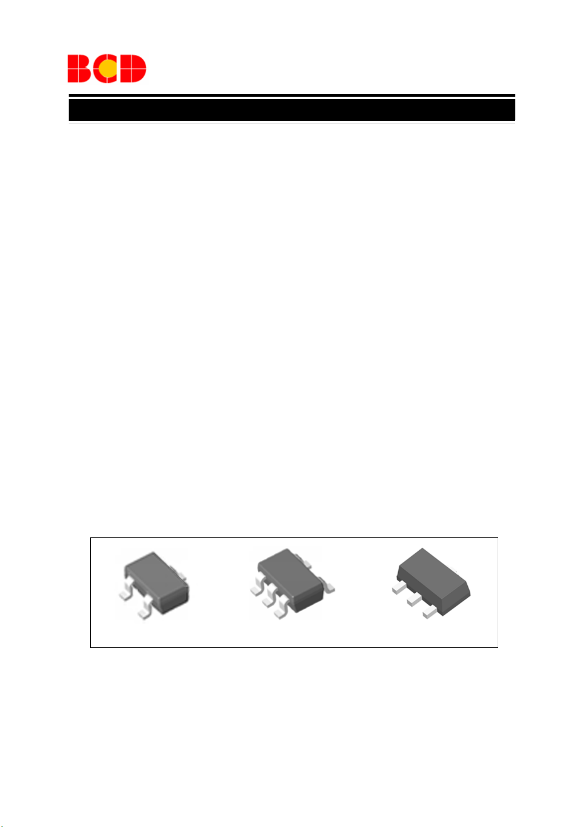
The AP2138 series is available in SOT-23-3 and SOT89 packages, AP2139 series is available in SOT-23-5
package.
· Battery Powered Equipment
· Reference Voltage Sources
· Cameras, Video Cameras
· Portable AV Systems
· Mobile Phones
· Communication Tools
· Portable Games
SOT-23-3
Figure 1. Package Types of AP2138/2139
Jul. 2012 Rev. 2. 3 BCD Semiconductor Manufacturing Limited
SOT-23-5
1
SOT-89
Page 2
Data Sheet
1
2
3
3
2
1
1
2
34
5
1
2
3
ULTRA LOW QUIESCENT CURRENT CMOS LDO AP2138/2139
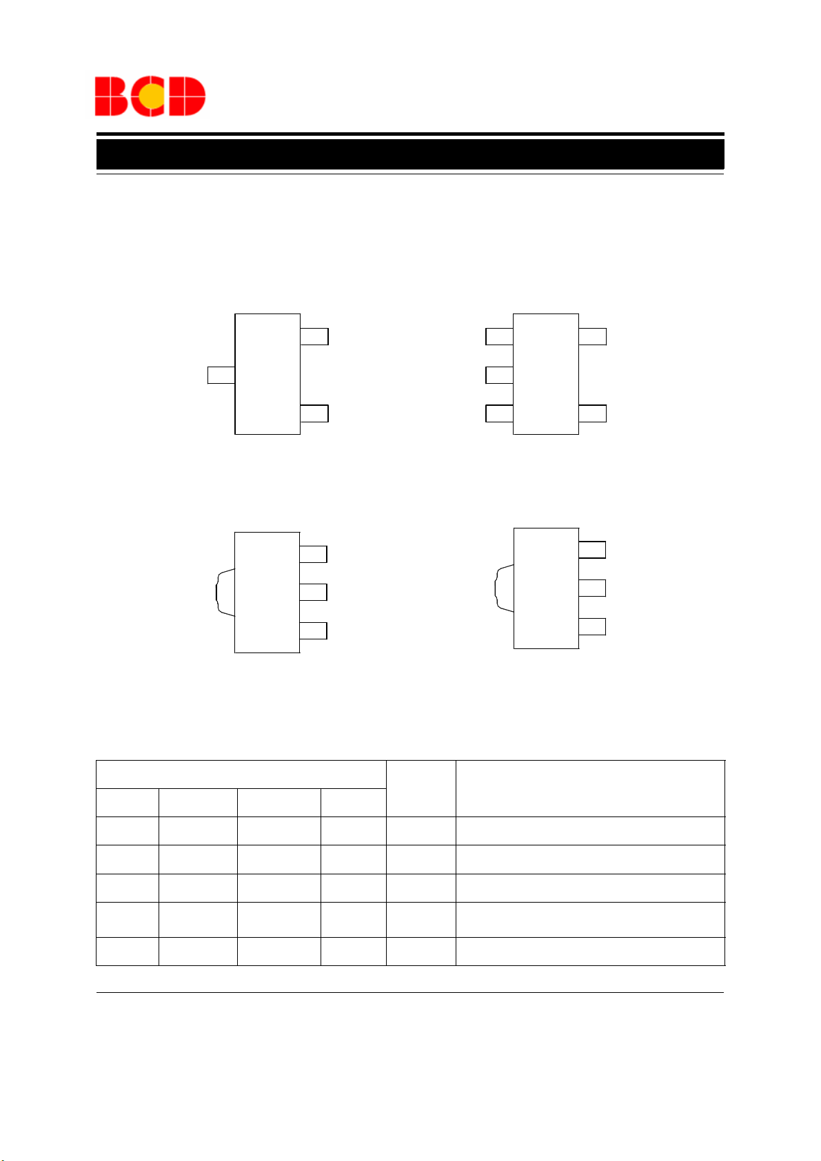
Pin Configuration
N Package
(SOT-23-3)
V
IN
R Package
(SOT-89)
K Package
(SOT-23-5)
V
OUT
GND
V
GND
CE
IN
RA Package
(SOT-89)
V
OUT
V
NC
OUT
V
IN
V
IN
GND
Figure 2. Pin Configuration of AP2138/2139 (Top View)
Pin Description
Pin Number
Pin Name Function
SOT-23-3 SOT-89 (R) SOT-89 (RA) SOT-23-5
1 1 2 2 GND Ground
23 1 5V
32 3 1V
3 CE Active high enable input. Logic high=enable, logic
4 NC No connection
OUT
IN
Regulated output voltage
Input voltage
low=shutdown
GND
V
OUT
Jul. 2012 Rev. 2. 3 BCD Semiconductor Manufacturing Limited
2
Page 3
Data Sheet
VREF
CURRENT
LIMIT
VREF
CURRENT LIMIT
ULTRA LOW QUIESCENT CURRENT CMOS LDO AP2138/2139
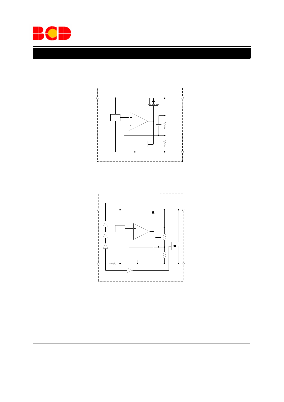
Functional Block Diagram
V
3 (2)[3]
IN
AP2138
2 (3)[1]
1 (1)[2]
V
OUT
GND
A(B)[C]
A: SOT-23-3
B: SOT-89 (R)
C: SOT-89 (RA)
V
IN
CE
1
3
5
2
GND
AP2139
Figure 3. Functional Block Diagram of AP2138/2139
V
OUT
Jul. 2012 Rev. 2. 3 BCD Semiconductor Manufacturing Limited
3
Page 4
Data Sheet
ULTRA LOW QUIESCENT CURRENT CMOS LDO AP2138/2139
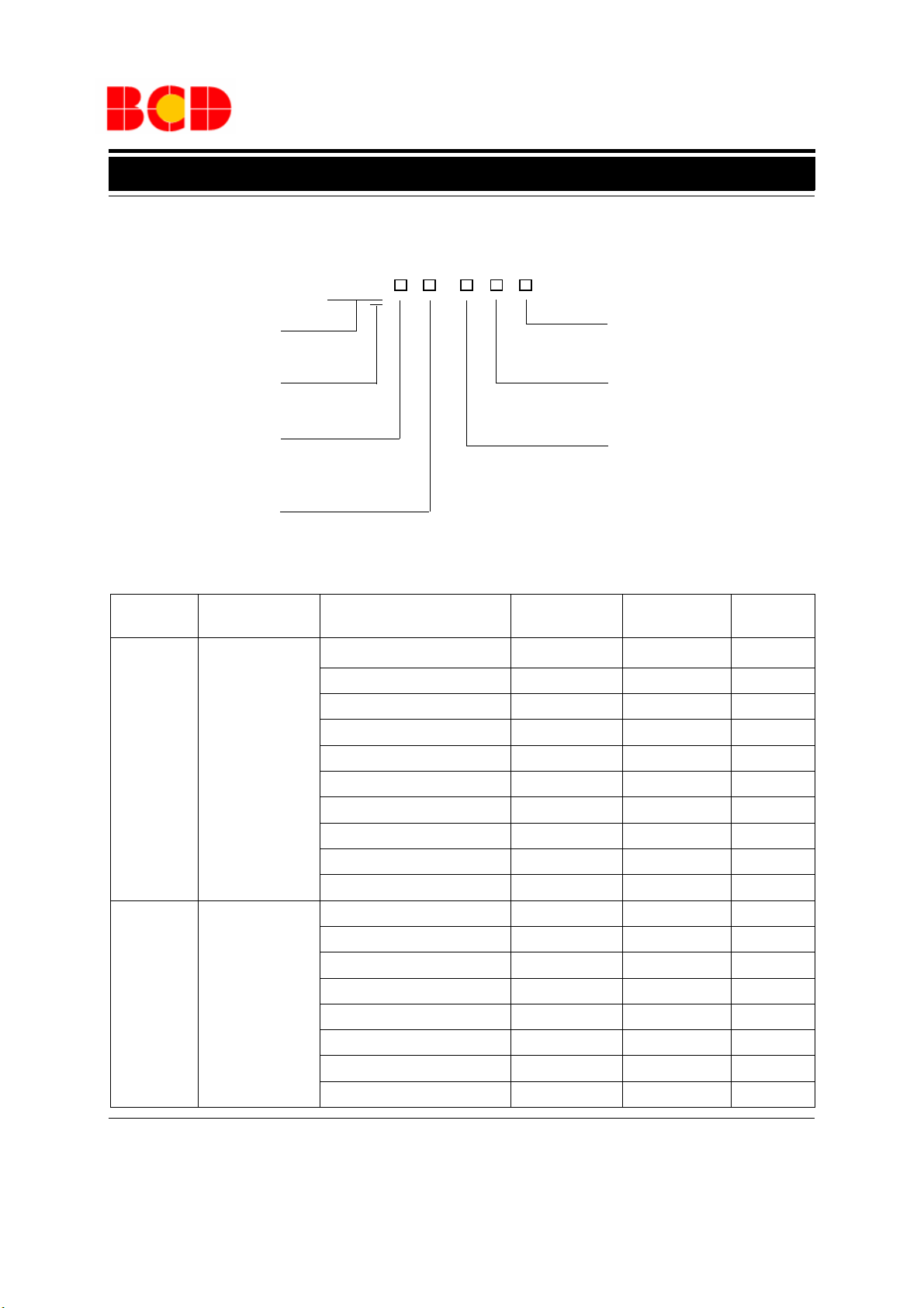
Ordering Information
G1: Green
TR: Tape and Reel
1.2: Fixed Output 1.2V
1.4: Fixed Output 1.4V
1.5: Fixed Output 1.5V
1.8: Fixed Output 1.8V
2.5: Fixed Output 2.5V
2.8: Fixed Output 2.8V
3.0: Fixed Output 3.0V
3.3: Fixed Output 3.3V
3.6: Fixed Output 3.6V
4.0: Fixed Output 4.0V
Condition Part Number Marking ID
Packing
Typ e
Circuit Type
8: AP2138
9: AP2139
A: Active High
with Built-in Resistor
Blank: No Enable Function
Package
N: SOT-23-3
K: SOT-23-5
R/RA: SOT-89
Package
Temperature
Range
AP213X -
SOT-23-3
SOT-89
-40 to 85
-40 to 85
1.2V
1.4V
1.5V
1.8V
o
C
o
C
2.5V
2.8V
3.0V
3.3V
3.6V
4.0V
1.2V(R) AP2138R-1.2TRG1 G42C Tape & Reel
1.4V (R)
1.5V (R)
1.8V (R)
2.5V (R)
2.8V (R)
3.0V (R)
3.3V (R)
AP2138N-1.2TRG1 GA3 Tape & Reel
AP2138N-1.4TRG1 GG1
AP2138N-1.5TRG1 GG2
AP2138N-1.8TRG1 GG4
AP2138N-2.5TRG1 GG5
AP2138N-2.8TRG1 GG6
AP2138N-3.0TRG1 GG3
AP2138N-3.3TRG1 GG7
AP2138N-3.6TRG1 GG8
AP2138N-4.0TRG1 GE9
AP2138R-1.4TRG1
AP2138R-1.5TRG1
AP2138R-1.8TRG1
AP2138R-2.5TRG1
AP2138R-2.8TRG1
AP2138R-3.0TRG1
AP2138R-3.3TRG1
G42D Tape & Reel
G42E Tape & Reel
G42F Tape & Reel
G42G Tape & Reel
G42H Tape & Reel
G42J Tape & Reel
G42K Tape & Reel
Tap e & Re el
Tap e & Re el
Tap e & Re el
Tap e & Re el
Tap e & Re el
Tap e & Re el
Tap e & Re el
Tap e & Re el
Tap e & Re el
Jul. 2012 Rev. 2. 3 BCD Semiconductor Manufacturing Limited
4
Page 5
Data Sheet
ULTRA LOW QUIESCENT CURRENT CMOS LDO AP2138/2139
Ordering Information (Continued)
Package Temperature Range Condition Part Number Marking ID
1.2V (RA) AP2138RA-1.2TRG1 G13L Tape & Reel
AP2138RA-1.4TRG1
AP2138RA-1.5TRG1
AP2138RA-1.8TRG1
AP2138RA-2.5TRG1
AP2138RA-2.8TRG1
AP2138RA-3.0TRG1
AP2138RA-3.3TRG1
G13M Tape & Reel
G13N Tape & Reel
G13O Tape & Reel
G13P Tape & Reel
G33J Tape & Reel
G37J Tape & Reel
G41J Tape & Reel
SOT-89
SOT-23-5
-40 to 85
-40 to 85
1.4V (RA)
1.5V (RA)
o
C
Active High with Built-in Resistor AP2139AK-1.2TRG1 G7R Tape & Reel
Active High with Built-in Resistor AP2139AK-1.4TRG1 G6L Tape & Reel
Active High with Built-in Resistor AP2139AK-1.5TRG1 G6M Tape & Reel
o
C
Active High with Built-in Resistor AP2139AK-1.8TRG1 G6N Tape & Reel
Active High with Built-in Resistor AP2139AK-2.5TRG1 G6P Tape & Reel
Active High with Built-in Resistor AP2139AK-2.8TRG1 G6Q Tape & Reel
Active High with Built-in Resistor AP2139AK-3.0TRG1 G6J Tape & Reel
Active High with Built-in Resistor AP2139AK-3.3TRG1 G6R Tape & Reel
1.8V (RA)
2.5V (RA)
2.8V (RA)
3.0V (RA)
3.3V (RA)
Packing
Typ e
BCD Semiconductor's products, as designated with "G1" suffix in the part number, are RoHS compliant and Green.
Jul. 2012 Rev. 2. 3 BCD Semiconductor Manufacturing Limited
5
Page 6
Data Sheet
ULTRA LOW QUIESCENT CURRENT CMOS LDO AP2138/2139
Absolute Maximum Ratings (Note 1)
Parameter Symbol Value Unit
Input Voltage V
Enable Input Voltage (AP2139) V
Lead Temperature T
Junction Temperature T
Storage Temperature Range T
IN
CE
LEAD
J
STG
ESD (Machine Model) ESD 350 V
ESD (Human Body Model) ESD 2000 V
SOT-23-3 250
Thermal Resistance (Note 2) θ
JA
SOT-23-5 250
SOT-89 165
Note 1: Stresses greater than those listed under "Absolute Maximum Ratings" may cause permanent damage to the device.
These are stress ratings only, and functional operation of the device at these or any other conditions beyond those indicated
under "Recommended Operating Conditions" is not implied. Exposure to "Absolute Maximum Ratings" for extended periods
may affect device reliability.
Note 2: Absolute maximum ratings indicate limits beyond which damage to the component may occur. Electrical specifications do not apply when operating the device outside of its operating ratings. The maximum allowable power dissipation is a
function of the maximum junction temperature, T
perature, T
)/θ
T
A
The maximum allowable power dissipation at any ambient temperature is calculated using: P
A.
Exceeding the maximum allowable power dissipation will result in excessive die temperature.
JA.
the junction-to-ambient thermal resistance, θ
J(max),
7.0 V
-0.3 to VIN+0.3 V
o
=(T
o
o
o
C/W
260
150
-65 to 150
and the ambient tem-
JA,
D(max)
C
C
C
J(max)
-
Recommended Operating Conditions
Parameter Symbol Min Max Unit
Input Voltage V
Operating Ambient Temperature Range
IN
T
A
Jul. 2012 Rev. 2. 3 BCD Semiconductor Manufacturing Limited
6
2.5 6.6 V
-40 85
o
C
Page 7
Data Sheet
ULTRA LOW QUIESCENT CURRENT CMOS LDO AP2138/2139
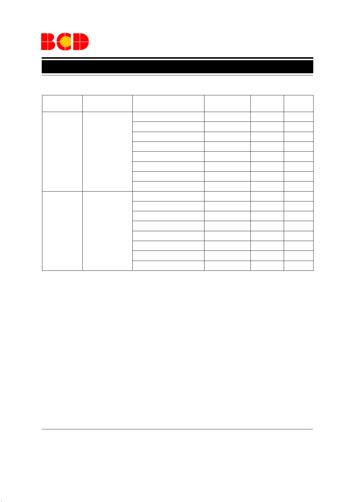
Electrical Characteristics
AP2138/2139-1.2 Electrical Characteristics
(VIN=2.5V, VCE=2.5V (AP2139),TJ=25oC, I
otherwise specified.)
Parameter Symbol Conditions Min Typ Max Unit
Input Voltage V
Output Voltage V
Quiescent Current I
Standby Current (AP2139) I
Output Current I
Load Regulation
=40mA, CIN=C
OUT
IN
OUT
Q
STD
OUT
V
RLOAD
=1μF,
Bold
OUT
typeface applies over -40oC
≤TJ≤
85oC,
6.6 V
1.176 1.200 1.224 V
I
=0 1.0 1.5 μA
OUT
VCE=0 0.1 1 μA
250 mA
1mA≤I
OUT
≤100mA
25 40 mV
unless
Line Regulation
Dropout Voltage
Output Voltage
Temperature Coefficient
Short Circuit Current
CE Pull-down Constant
Current (AP2139)
CE Input Logic-high
Voltage (AP2139)
CE Input Logic-low
Voltage (AP2139)
Thermal Resistance
(ΔV
V
RLINE
V
DROP
ΔV
OUT
OUT/VOUT
I
SHORT
I
PD
V
IH
V
IL
θ
JC
/ΔT
)/ΔT
2.2V≤VIN≤6V
I
=10mA 100 300
OUT
I
=30mA 400 700
OUT
=100mA 700 1000
I
OUT
I
=250mA 1000 1300
OUT
618mV
±140
±100
V
=0
OUT
1.2 V
SOT-23-3 81.9
SOT-23-5 81.9
SOT-89 51.1
50 mA
0.2 μA
mV
μV/
ppm/
0.3 V
o
C/W
o
C
o
C
Jul. 2012 Rev. 2. 3 BCD Semiconductor Manufacturing Limited
7
Page 8

Data Sheet
ULTRA LOW QUIESCENT CURRENT CMOS LDO AP2138/2139
Electrical Characteristics(Continued)
AP2138/2139-1.4 Electrical Characteristics
(VIN=2.5V, VCE=2.5V (AP2139),TJ=25oC, I
otherwise specified.)
Parameter Symbol Conditions Min Typ Max Unit
Input Voltage V
Output Voltage V
Quiescent Current I
Standby Current (AP2139) I
Output Current I
Load Regulation
Line Regulation
Dropout Voltage
Output Voltage
Temperature Coefficient
(ΔV
Short Circuit Current
=40mA, CIN=C
OUT
IN
OUT
Q
STD
OUT
V
RLOAD
V
RLINE
V
DROP
ΔV
OUT
OUT/VOUT
I
SHORT
/ΔT
)/ΔT
=1μF,
Bold
OUT
typeface applies over -40oC
≤TJ≤
85oC,
6.6 V
1.372 1.400 1.428 V
I
=0 1.0 1.5 μA
OUT
VCE=0 0.1 1 μA
250 mA
1mA≤I
2.4V≤VIN≤6V
I
OUT
I
OUT
I
OUT
I
OUT
V
OUT
OUT
≤100mA
25 40 mV
618mV
=10mA 100 300
=30mA 400 700
=100mA 600 900
=250mA 1000 1300
±140
±100
=0
50 mA
mV
μV/
ppm/
unless
o
C
o
C
CE Pull-down Constant
Current (AP2139)
CE Input Logic-high
Voltage (AP2139)
CE Input Logic-low
Voltage (AP2139)
I
PD
V
IH
V
IL
1.2 V
0.2 μA
0.3 V
SOT-23-3 81.9
Thermal Resistance
θ
JC
SOT-23-5 81.9
o
C/W
SOT-89 51.1
Jul. 2012 Rev. 2. 3 BCD Semiconductor Manufacturing Limited
8
Page 9

Data Sheet
ULTRA LOW QUIESCENT CURRENT CMOS LDO AP2138/2139
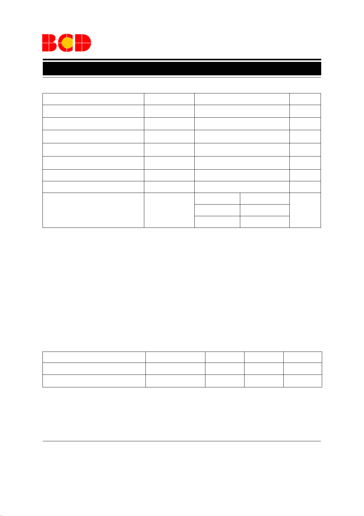
Electrical Characteristics (Continued)
AP2138/2139-1.5 Electrical Characteristics
(VIN=2.5V, VCE=2.5V (AP2139),TJ=25oC, I
otherwise specified.)
Parameter Symbol Conditions Min Typ Max Unit
Input Voltage V
Output Voltage V
Quiescent Current I
Standby Current (AP2139) I
Output Current I
Load Regulation
=40mA, CIN=C
OUT
IN
OUT
Q
STD
OUT
V
RLOAD
=1μF,
Bold
OUT
typeface applies over -40oC
≤TJ≤
85oC,
6.6 V
1.470 1.500 1.530 V
I
=0 1.0 1.5 μA
OUT
VCE=0 0.1 1 μA
250 mA
1mA≤I
OUT
≤100mA
25 40 mV
unless
Line Regulation
Dropout Voltage
Output Voltage
Temperature Coefficient
Short Circuit Current
CE Pull-down Constant
Current (AP2139)
CE Input Logic-high
Voltage (AP2139)
CE Input Logic-low
Voltage (AP2139)
Thermal Resistance
(ΔV
V
RLINE
V
DROP
ΔV
OUT
OUT/VOUT
I
SHORT
I
PD
V
IH
V
IL
θ
JC
/ΔT
)/ΔT
2.5V≤VIN≤6V
I
=10mA 100 300
OUT
I
=30mA 200 400
OUT
=100mA 600 900
I
OUT
I
=250mA 1000 1300
OUT
618 mV
±150
±100
V
=0
OUT
1.2 V
SOT-23-3 81.9
SOT-23-5 81.9
SOT-89 51.1
50 mA
0.2 μA
mV
μV/
ppm/
0.3 V
o
C/W
o
C
o
C
Jul. 2012 Rev. 2. 3 BCD Semiconductor Manufacturing Limited
9
Page 10

Data Sheet
ULTRA LOW QUIESCENT CURRENT CMOS LDO AP2138/2139
Electrical Characteristics (Continued)
AP2138/2139-1.8 Electrical Characteristics
(VIN=2.8V, VCE=2.8V (AP2139),TJ=25oC, I
otherwise specified.)
Parameter Symbol Conditions Min Typ Max Unit
Input Voltage V
Output Voltage V
Quiescent Current I
Standby Current (AP2139) I
Output Current I
Load Regulation
Line Regulation
Dropout Voltage
Output Voltage
Temperature Coefficient
(ΔV
Short Circuit Current
=40mA, CIN=C
OUT
IN
OUT
Q
STD
OUT
V
RLOAD
V
RLINE
V
DROP
ΔV
OUT
OUT/VOUT
I
SHORT
/ΔT
)/ΔT
=1μF,
Bold
OUT
typeface applies over -40oC
≤TJ≤
85oC,
6.6 V
1.764 1.800 1.836 V
I
=0 1.0 1.5 μA
OUT
VCE=0 0.1 1 μA
250 mA
1mA≤I
2.8V≤VIN≤6V
I
OUT
I
OUT
I
OUT
I
OUT
V
OUT
OUT
≤100mA
25 40 mV
618 mV
=10mA 25 100
=30mA 120 250
=100mA 400 700
=250mA 850 1100
±180
±100
=0
50 mA
mV
μV/
ppm/
unless
o
C
o
C
CE Pull-down Constant
Current (AP2139)
CE Input Logic-high
Voltage (AP2139)
CE Input Logic-low
Voltage (AP2139)
I
PD
V
IH
V
IL
1.2 V
0.2 μA
0.3 V
SOT-23-3 81.9
Thermal Resistance
θ
JC
SOT-23-5 81.9
o
C/W
SOT-89 51.1
Jul. 2012 Rev. 2. 3 BCD Semiconductor Manufacturing Limited
10
Page 11

Data Sheet
ULTRA LOW QUIESCENT CURRENT CMOS LDO AP2138/2139
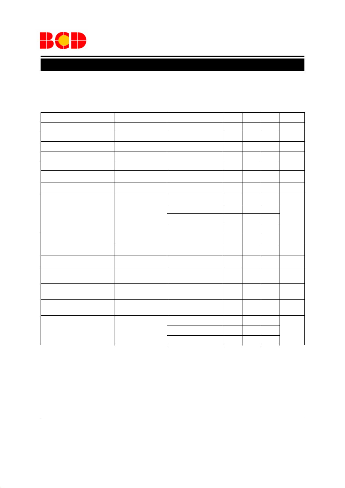
Electrical Characteristics (Continued)
AP2138/2139-2.5 Electrical Characteristics
(VIN=3.5V, VCE=3.5V (AP2139), TJ=25oC, I
otherwise specified.)
Parameter Symbol Conditions Min Typ Max Unit
Input Voltage V
Output Voltage V
Quiescent Current I
Standby Current (AP2139) I
Output Current I
Load Regulation
=40mA, CIN=C
OUT
IN
OUT
Q
STD
OUT
V
RLOAD
=1μF,
Bold
OUT
typeface applies over -40oC
≤TJ≤
85oC,
6.6 V
2.450 2.500 2.550 V
I
=0 1.0 1.5 μA
OUT
VCE=0 0.1 1 μA
250 mA
1mA≤I
OUT
≤100mA
25 40 mV
unless
Line Regulation
Dropout Voltage
Output Voltage
Temperature Coefficient
Short Circuit Current
CE Pull-down Constant
Current (AP2139)
CE Input Logic-high
Voltage (AP2139)
CE Input Logic-low
Voltage (AP2139)
Thermal Resistance
(ΔV
V
RLINE
V
DROP
ΔV
OUT
OUT/VOUT
I
SHORT
I
PD
V
IH
V
IL
θ
JC
/ΔT
)/ΔT
3.5V≤VIN≤6V
I
=10mA 25 100
OUT
I
=30mA 100 250
OUT
=100mA 250 500
I
OUT
I
=250mA 650 1000
OUT
618 mV
±250
±100
V
=0
OUT
1.2 V
SOT-23-3 81.9
SOT-23-5 81.9
SOT-89 51.1
50 mA
0.2 μA
mV
μV/
ppm/
0.3 V
o
C/W
o
C
o
C
Jul. 2012 Rev. 2. 3 BCD Semiconductor Manufacturing Limited
11
Page 12

Data Sheet
ULTRA LOW QUIESCENT CURRENT CMOS LDO AP2138/2139
Electrical Characteristics (Continued)
AP2138/2139-2.8 Electrical Characteristics
(VIN=3.8V, VCE=3.8V (AP2139), TJ=25oC, I
otherwise specified.)
Parameter Symbol Conditions Min Typ Max Unit
Input Voltage V
Output Voltage V
Quiescent Current I
Standby Current (AP2139) I
Output Current I
Load Regulation
Line Regulation
Dropout Voltage
Output Voltage
Temperature Coefficient
(ΔV
Short Circuit Current
=40mA, CIN=C
OUT
IN
OUT
Q
STD
OUT
V
RLOAD
V
RLINE
V
DROP
ΔV
OUT
OUT/VOUT
I
SHORT
/ΔT
)/ΔT
=1μF,
Bold
OUT
typeface applies over -40oC
≤TJ≤
85oC,
6.6 V
2.744 2.800 2.856 V
I
=0 1.0 1.5 μA
OUT
VCE=0 0.1 1 μA
250 mA
1mA≤I
3.8V≤VIN≤6V
I
OUT
I
OUT
I
OUT
I
OUT
V
OUT
OUT
≤100mA
25 40 mV
618 mV
=10mA 25 100
=30mA 70 200
=100mA 250 500
=250mA 500 800
±280
±100
=0
50 mA
mV
μV/
ppm/
unless
o
C
o
C
CE Pull-down Constant
Current (AP2139)
CE Input Logic-high
Voltage (AP2139)
CE Input Logic-low
Voltage (AP2139)
I
PD
V
IH
V
IL
1.2 V
0.2 μA
0.3 V
SOT-23-3 81.9
Thermal Resistance
θ
JC
SOT-23-5 81.9
o
C/W
SOT-89 51.1
Jul. 2012 Rev. 2. 3 BCD Semiconductor Manufacturing Limited
12
Page 13

Data Sheet
ULTRA LOW QUIESCENT CURRENT CMOS LDO AP2138/2139
Electrical Characteristics (Continued)
AP2138/2139-3.0 Electrical Characteristics
(VIN=4V, VCE=4V (AP2139), TJ=25oC, I
erwise specified.)
Parameter Symbol Conditions Min Typ Max Unit
Input Voltage V
Output Voltage V
Quiescent Current I
Standby Current (AP2139) I
Output Current I
Load Regulation
=40mA, CIN=C
OUT
IN
OUT
Q
STD
OUT
V
RLOAD
=1μF,
Bold
OUT
typeface applies over -40oC
≤TJ≤
85oC,
unless oth-
6.6 V
2.940 3.000 3.060 V
I
=0 1.0 1.5 μA
OUT
VCE=0 0.1 1 μA
250 mA
1mA≤I
OUT
≤100mA
25 40 mV
Line Regulation
Dropout Voltage
Output Voltage
Temperature Coefficient
Short Circuit Current
CE Pull-down Constant
Current (AP2139)
CE Input Logic-high
Voltage (AP2139)
CE Input Logic-low
Voltage (AP2139)
Thermal Resistance
(ΔV
V
RLINE
V
DROP
ΔV
OUT
OUT/VOUT
I
SHORT
I
PD
V
IH
V
IL
θ
JC
/ΔT
)/ΔT
4V≤VIN≤6V
I
=10mA 25 100
OUT
I
=30mA 70 200
OUT
I
=100mA 200 400
OUT
=250mA 450 700
I
OUT
618mV
±300
±100
V
=0
OUT
1.2 V
SOT-23-3 81.9
SOT-23-5 81.9
SOT-89 51.1
50 mA
0.2 μA
mV
μV/
ppm/
0.3 V
o
C/W
o
C
o
C
Jul. 2012 Rev. 2. 3 BCD Semiconductor Manufacturing Limited
13
Page 14

Data Sheet
ULTRA LOW QUIESCENT CURRENT CMOS LDO AP2138/2139
Electrical Characteristics (Continued)
AP2138/2139-3.3 Electrical Characteristics
(VIN=4.3V, VCE=4.3V (AP2139),TJ=25oC, I
otherwise specified.)
Parameter Symbol Conditions Min Typ Max Unit
Input Voltage V
Output Voltage V
Quiescent Current I
Standby Current (AP2139) I
Output Current I
Load Regulation
Line Regulation
Dropout Voltage
Output Voltage
Temperature Coefficient
(ΔV
Short Circuit Current
=40mA, CIN=C
OUT
IN
OUT
Q
STD
OUT
V
RLOAD
V
RLINE
V
DROP
ΔV
OUT
OUT/VOUT
I
SHORT
/ΔT
)/ΔT
=1μF,
Bold
OUT
typeface applies over -40oC
≤TJ≤
85oC,
6.6 V
3.234 3.300 3.366 V
I
=0 1.0 1.5 μA
OUT
VCE=0 0.1 1 μA
250 mA
1mA≤I
4.3V≤VIN≤6V
I
OUT
I
OUT
I
OUT
I
OUT
V
OUT
OUT
≤100mA
25 40 mV
618mV
=10mA 20 100
=30mA 50 200
=100mA 160 300
=250mA 400 600
±330
±100
=0
50 mA
mV
μV/
ppm/
unless
o
C
o
C
CE Pull-down Constant
Current (AP2139)
CE Input Logic-high
Voltage (AP2139)
CE Input Logic-low
Voltage (AP2139)
I
PD
V
IH
V
IL
1.2 V
0.2 μA
0.3 V
SOT-23-3 81.9
Thermal Resistance
θ
JC
SOT-23-5 81.9
o
C/W
SOT-89 51.1
Jul. 2012 Rev. 2. 3 BCD Semiconductor Manufacturing Limited
14
Page 15

Data Sheet
ULTRA LOW QUIESCENT CURRENT CMOS LDO AP2138/2139
Electrical Characteristics (Continued)
AP2138-3.6 Electrical Characteristics
(VIN=4.6V, TJ=25oC, I
Parameter Symbol Conditions Min Typ Max Unit
Input Voltage V
Output Voltage V
Quiescent Current I
Output Current I
Load Regulation
=40mA, CIN=C
OUT
OUT
V
RLOAD
=1μF,
IN
OUT
Q
OUT
Bold
typeface applies over -40oC
I
=0 1.0 1.5 μA
OUT
1mA≤I
OUT
≤100mA
≤TJ≤
85oC,
unless otherwise specified.)
6.6 V
3.528 3.600 3.672 V
250 mA
25 40 mV
Line Regulation
Dropout Voltage
Output Voltage
Temperature Coefficient
Short Circuit Current
Thermal Resistance
(ΔV
V
RLINE
V
DROP
ΔV
OUT
OUT/VOUT
I
SHORT
θ
JC
/ΔT
)/ΔT
4.6V≤VIN≤6V
I
=10mA 20 100
OUT
I
=30mA 50 200
OUT
=100mA 160 300
I
OUT
I
=250mA 400 600
OUT
618mV
±330
±100
V
=0
OUT
SOT-23-3 81.9
SOT-23-5 81.9
SOT-89 51.1
50 mA
mV
μV/
ppm/
o
C/W
o
C
o
C
Jul. 2012 Rev. 2. 3 BCD Semiconductor Manufacturing Limited
15
Page 16

Data Sheet
ULTRA LOW QUIESCENT CURRENT CMOS LDO AP2138/2139
Electrical Characteristics (Continued)
AP2138-4.0 Electrical Characteristics
(VIN=5.0V, TJ=25oC, I
Parameter Symbol Conditions Min Typ Max Unit
Input Voltage V
Output Voltage V
Quiescent Current I
Output Current I
Load Regulation
Line Regulation
Dropout Voltage
Output Voltage
Temperature Coefficient
Short Circuit Current
=40mA, CIN=C
OUT
(ΔV
=1μF,
OUT
IN
OUT
Q
OUT
V
RLOAD
V
RLINE
V
DROP
ΔV
OUT
OUT/VOUT
I
SHORT
Bold
typeface applies over -40oC
I
=0 1.0 1.5 μA
OUT
1mA≤I
5V≤VIN≤6V
I
=10mA 20 100
OUT
I
=30mA 50 200
OUT
I
=100mA 160 300
OUT
I
=250mA 400 600
OUT
/ΔT
)/ΔT
V
OUT
OUT
=0
≤100mA
≤TJ≤
85oC,
unless otherwise specified.)
6.6 V
3.920 4.000 4.080 V
250 mA
25 40 mV
618mV
±330
±100
50 mA
mV
μV/
ppm/
o
C
o
C
SOT-23-3 81.9
Thermal Resistance
θ
JC
SOT-23-5 81.9
o
C/W
SOT-89 51.1
Jul. 2012 Rev. 2. 3 BCD Semiconductor Manufacturing Limited
16
Page 17

Data Sheet
-40-200 20406080100120
3.20
3.22
3.24
3.26
3.28
3.30
3.32
3.34
3.36
3.38
3.40
AP2138-3.3
Output Voltage (V)
Junction Temperature(oC)
I
OUT
=10mA
I
OUT
=100mA
I
OUT
=150mA
I
OUT
=200mA
I
OUT
=250mA
0 25 50 75 100 125 150 175 200 225 250
3.20
3.22
3.24
3.26
3.28
3.30
3.32
3.34
3.36
3.38
3.40
AP2138-3.3
V
IN
=4.3V
T
J
=25oC
Output Voltage (V)
Output Current (mA)
012345678
0.0
0.2
0.4
0.6
0.8
1.0
1.2
1.4
1.6
AP2138-3.3
No Load
TJ=-40oC
TJ=25oC
TJ=85oC
Quiescent Current(μA)
Input Voltage (V)
0.0 0.5 1.0 1.5 2.0 2.5 3.0 3 .5 4.0 4.5 5.0 5.5 6.0 6.5
0.0
0.5
1.0
1.5
2.0
2.5
3.0
3.5
4.0
AP2138-3.3
No load
TJ=-40oC
TJ=25oC
TJ=85oC
Output Voltage (V)
Input Voltage (V)
ULTRA LOW QUIESCENT CURRENT CMOS LDO AP2138/2139
Typical Performance Characteristics
Figure 4. Output Voltage vs. Input Voltage
Figure 6. Output Voltage vs. Output Current
Jul. 2012 Rev. 2. 3 BCD Semiconductor Manufacturing Limited
Figure 5. Output Voltage vs. Junction Temperature
Figure 7.
Quiescent Current vs. Input Voltage
17
Page 18

Data Sheet
-40 -20 0 20 40 60 80
0.0
0.2
0.4
0.6
0.8
1.0
1.2
1.4
1.6
1.8
2.0
AP2138-3.3
V
IN
=4.3V
No Load
Quiescent Current (μA)
Junction Temperature(oC)
0 25 50 75 100 125 150 175 200 225 250
0
5
10
15
20
25
30
35
40
45
50
AP2138-3.3
V
IN
=4.3V
TJ=-40oC
TJ=25oC
TJ=85oC
Quiescent Current (μA)
Output Current (mA)
0 50 100 150 200 250 300 350 400 450 500 550 600
0.0
0.5
1.0
1.5
2.0
2.5
3.0
3.5
4.0
TJ=-40oC
TJ=25oC
TJ=85oC
AP2138-3.3
V
IN
=4.3V
Output Voltage (V)
Output Current (mA)
0 50 100 150 200 250 300 350 400 4 50 500 550 600
0.0
0.5
1.0
1.5
2.0
2.5
3.0
3.5
4.0
AP2138-3.3
T
J
=25oC
Output Voltage (V)
Output Current (mA)
VIN=3.8V
VIN=4.3V
VIN=6V
VIN=6.5V
ULTRA LOW QUIESCENT CURRENT CMOS LDO AP2138/2139
Typical Performance Characteristics (Continued)
Figure 8. Quiescent Current vs. Junction Temperature
Figure 9. Quiescent Current vs. Output Current
Figure 10. Output Voltage vs. Output Current
Jul. 2012 Rev. 2. 3 BCD Semiconductor Manufacturing Limited
Figure 11. Output Voltage vs. Output Current
18
Page 19

Data Sheet
0 25 50 75 100 125 150 175 200 225 250
0
50
100
150
200
250
300
350
400
450
500
550
600
AP2138-3.3
Dropout Voltage (mV)
Output Current (mA)
TJ=-40oC
TJ=25oC
TJ=85oC
-40-20 0 20406080
0
50
100
150
200
250
300
350
400
450
500
550
I
OUT
=250mA
I
OUT
=200mA
I
OUT
=150mA
I
OUT
=100mA
AP2138-3.3
Dropout Voltage (mV)
Junction Temperature (oC)
I
OUT
=10mA
ULTRA LOW QUIESCENT CURRENT CMOS LDO AP2138/2139
Typical Performance Characteristics (Continued)
Figure 12. Dropout Voltage vs. Output Current
V
IN
500mV
V
OUT
200mV/div
Time 100μs/div
Figure 14. Line transient (VIN=4.3 to 5.3V, I
OUT
=10mA)
Figure 13. Dropout Voltage vs. Junction Temperature
V
OUT
1V/div
I
OUT
50mA/div
Time 2ms/div
Figure 15. Load transient (V
=4.3V, I
IN
=1mA to150mA)
OUT
Jul. 2012 Rev. 2. 3 BCD Semiconductor Manufacturing Limited
19
Page 20

Data Sheet
Time 200μs/div
Time 200μs/div
ULTRA LOW QUIESCENT CURRENT CMOS LDO AP2138/2139
Typical Performance Characteristics (Continued)
V
V
1V/div
V
OUT
1V/div
IN
V
1V/div
Figure 16. Start-up Response
IN
1V/div
OUT
Figure 17. Enable Input Response
Jul. 2012 Rev. 2. 3 BCD Semiconductor Manufacturing Limited
20
Page 21

Data Sheet
V
IN
AP2138-1.4
C
IN
1μF
C
OUT
1μF
V
OUT
V
IN
V
OUT
GND
VIN=2.4V
V
OUT
=1.4V
V
IN
AP2139-3.0
C
IN
1μF
C
OUT
1μF
V
OUT
V
IN
V
OUT
GND
CE
NC
V
OUT
=3VVIN=4V
ULTRA LOW QUIESCENT CURRENT CMOS LDO AP2138/2139
Typical Application
Note: Filter capacitors are required at the AP2138/2139's input and output. 1μF capacitor is required at the input.
The minimum output capacitance required for stability should be more than 1μF with ESR from 0.01Ω to 100Ω.
Ceramic capacitors are recommended.
Figure 18. Typical Application of AP2138/2139
Jul. 2012 Rev. 2. 3 BCD Semiconductor Manufacturing Limited
21
Page 22

Data Sheet
2.820(0.111)
3.020(0.119)
2.650(0.104)
2.950(0.116)
0.950(0.037)
TYP
0.300(0.012)
0.500(0.020)
1.500(0.059)
1.700(0.067)
1.800(0.071)
2.000(0.079)
0.300(0.012)
0.600(0.024)
0.100(0.004)
0.200(0.008)
0.000(0.000)
0.150(0.006)
0.900(0.035)
1.300(0.051)
1.450(0.057)
MAX.
0.200(0.008)
0
8
ULTRA LOW QUIESCENT CURRENT CMOS LDO AP2138/2139
Mechanical Dimensions
SOT-23-3 Unit: mm(inch)
°
°
Jul. 2012 Rev. 2. 3 BCD Semiconductor Manufacturing Limited
22
Page 23

Data Sheet
2.820(0.111)
2
.
6
5
0
(
0
.
1
0
4
)
1
.
5
0
0
(
0
.
0
5
9
)
0
.
0
0
0
(
0
.
0
0
0
)
0.300(0.012)
0.950(0.037)
0
.
9
0
0
(
0
.
0
3
5
)
0.100(0.004)
0.200(0.008)
0
.
3
0
0
(
0
.
0
1
2
)
8°
0°
3.020(0.119)
1
.
7
0
0
(
0
.
0
6
7
)
2
.
9
5
0
(
0
.
1
1
6
)
0.400(0.016)
0
.
1
5
0
(
0
.
0
0
6
)
1
.
3
0
0
(
0
.
0
5
1
)
0.200(0.008)
0
.
6
0
0
(
0
.
0
2
4
)
1.800(0.071)
2.000(0.079)
0
.
7
0
0
(
0
.
0
2
8
)
R
E
F
T
Y
P
1
.
4
5
0
(
0
.
0
5
7
)
M
A
X
ULTRA LOW QUIESCENT CURRENT CMOS LDO AP2138/2139
Mechanical Dimensions (Continued)
SOT-23-5 Unit: mm(inch)
Jul. 2012 Rev. 2. 3 BCD Semiconductor Manufacturing Limited
23
Page 24

Data Sheet
45
1.030(0.041)REF
1.550(0.061)REF
4.400(0.173)
4.600(0.181)
0.900(0.035)
1.100(0.043)
3.950(0.156)
4.250(0.167)
3.000(0.118)
TYP
0.480(0.019)
2.300(0.091)
2.600(0.102)
0.320(0.013)
0.520(0.020)
3
10
2.060(0.081)REF
1.400(0.055)
1.600(0.063)
0.350(0.014)
0.450(0.018)
R0.150(0.006)
3
10
1.500(0.059)
0.320(0.013)REF
1.620(0.064)REF
2.210(0.087)REF
0.320(0.013)
0.520(0.020)
1.800(0.071)
ULTRA LOW QUIESCENT CURRENT CMOS LDO AP2138/2139
Mechanical Dimensions (Continued)
SOT-89 Unit: mm(inch)
Jul. 2012 Rev. 2. 3 BCD Semiconductor Manufacturing Limited
24
Page 25

BCD Semiconductor Manufacturing Limited
IMPORTANT NOTICE
IMPORTANT NOTICE
BCD Semiconductor Manufacturing Limited reserves the right to make changes without further notice to any products or specifi-
BCD Semiconductor Manufacturing Limited reserves the right to make changes without further notice to any products or specifi-
cations herein. BCD Semiconductor Manufacturing Limited does not assume any responsibility for use of any its products for any
cations herein. BCD Semiconductor Manufacturing Limited does not assume any responsibility for use of any its products for any
particular purpose, nor does BCD Semiconductor Manufacturing Limited assume any liability arising out of the application or use
particular purpose, nor does BCD Semiconductor Manufacturing Limited assume any liability arising out of the application or use
of any its products or circuits. BCD Semiconductor Manufacturing Limited does not convey any license under its patent rights or
of any its products or circuits. BCD Semiconductor Manufacturing Limited does not convey any license under its patent rights or
other rights nor the rights of others.
other rights nor the rights of others.
http://www.bcdsemi.com
MAIN SITE
MAIN SITE
- Headquarters
BCD Semiconductor Manufacturing Limited
BCD Semiconductor Manufactur ing Limited
- Wafer Fab
No. 1600, Zi Xing Road, Shanghai ZiZhu Science-based Industrial Park, 200241, China
Shanghai SIM-BCD Semiconductor Manufacturing Limited
Tel: +86-21-24162266, Fax: +86-21-24162277
800, Yi Shan Road, Shanghai 200233, China
Tel: +86-21-6485 1491, Fax: +86-21-5450 0008
REGIONAL SALES OFFICE
Shenzhen Office
REGIONAL SALES OFFICE
Shanghai SIM-BCD Semiconductor Manufacturing Co., Ltd., Shenzhen Office
Shenzhen Office
Unit A Room 1203, Skyworth Bldg., Gaoxin Ave.1.S., Nanshan District, Shenzhen,
Shanghai SIM-BCD Semiconductor Manufacturing Co., Ltd. Shenzhen Office
China
Advanced Analog Circuits (Shanghai) Corporation Shenzhen Office
Tel: +86-755-8826 7951
Room E, 5F, Noble Center, No.1006, 3rd Fuzhong Road, Futian District, Shenzhen 518026, China
Fax: +86-755-8826 7865
Tel: +86-755-8826 7951
Fax: +86-755-8826 7865
- Wafer Fab
BCD Semiconductor Manufacturing Limited
Shanghai SIM-BCD Semiconductor Manufacturing Co., Ltd.
- IC Design Group
800 Yi Shan Road, Shanghai 200233, China
Advanced Analog Circuits (Shanghai) Corporation
Tel: +86-21-6485 1491, Fax: +86-21-5450 0008
8F, Zone B, 900, Yi Shan Road, Shanghai 200233, China
Tel: +86-21-6495 9539, Fax: +86-21-6485 9673
Taiwan Office
BCD Semiconductor (Taiwan) Company Limited
Taiwan Office
4F, 298-1, Rui Guang Road, Nei-Hu District, Taipei,
BCD Semiconductor (Taiwan) Company Limited
Tai wan
4F, 298-1, Rui Guang Road, Nei-Hu District, Taipei,
Tel: +886-2-2656 2808
Taiwan
Fax: +886-2-2656 2806
Tel: +886-2-2656 2808
Fax: +886-2-2656 2806
USA Office
BCD Semiconductor Corp.
USA Office
30920 Huntwood Ave. Hayward,
BCD Semiconductor Corporation
CA 94544, USA
30920 Huntwood Ave. Hayward,
Tel : +1-510-324-2988
CA 94544, U.S.A
Fax: +1-510-324-2788
Tel : +1-510-324-2988
Fax: +1-510-324-2788
 Loading...