

Page 1

Data Sheet
300mA HIGH SPEED, EXTREMELY LOW NOISE CMOS LDO REGULATOR AP2128
General Description
The AP2128 series are positive voltage regulator ICs
fabricated by CMOS process. The AP2128 provides
two kinds of output voltage operation modes for
setting the output voltage. Fixed output voltage mode
senses the output voltage on V
voltage mode needs two resistors as a voltage divider.
The AP2128 series have features of low dropout
voltage, low noise, high output voltage accuracy, and
low current consumption which
use in various battery-powered devices.
AP2128 have 1.0V, 1.2V, 1.5V, 1.8V, 2.5V, 2.8V, 3.0V,
3.3V, 3.9V, 4.2V, 4.75V, 5.2V fixed voltage versions
and 0.8V to 5.5V adjustable voltage version.
AP2128 series are available in SOT-23-5 package.
, adjustable output
OUT
make them ideal for
Features
· Wide Operating Voltage: 2.5V to 6V
· Low
Dropout Voltage:170mV@300mA for
V
=3.3V, 140mV@300mA for V
OUT
OUT
=5.2V
· High Output Voltage Accuracy: ±2%
· High Ripple Rejection:
68dB@ f=1kHz, 54dB@ f=10kHz
· Low Standby Current: 0.1µA
· Low Quiescent Current: 60µA Typical
· Low Output Noise: 60µVrms @V
OUT
=0.8V
· Short Current Limit: 50mA
· Over Temperature Protection
· Compatible with Low ESR Ceramic Capacitor:
1µF for C
and C
IN
OUT
· Excellent Line/Load Regulation
· Soft Start Time: 50µs
· Auto Discharge Resistance: R
DS(ON)
=60Ω
Applications
· Datacom
· Notebook Computers
· Mother Board
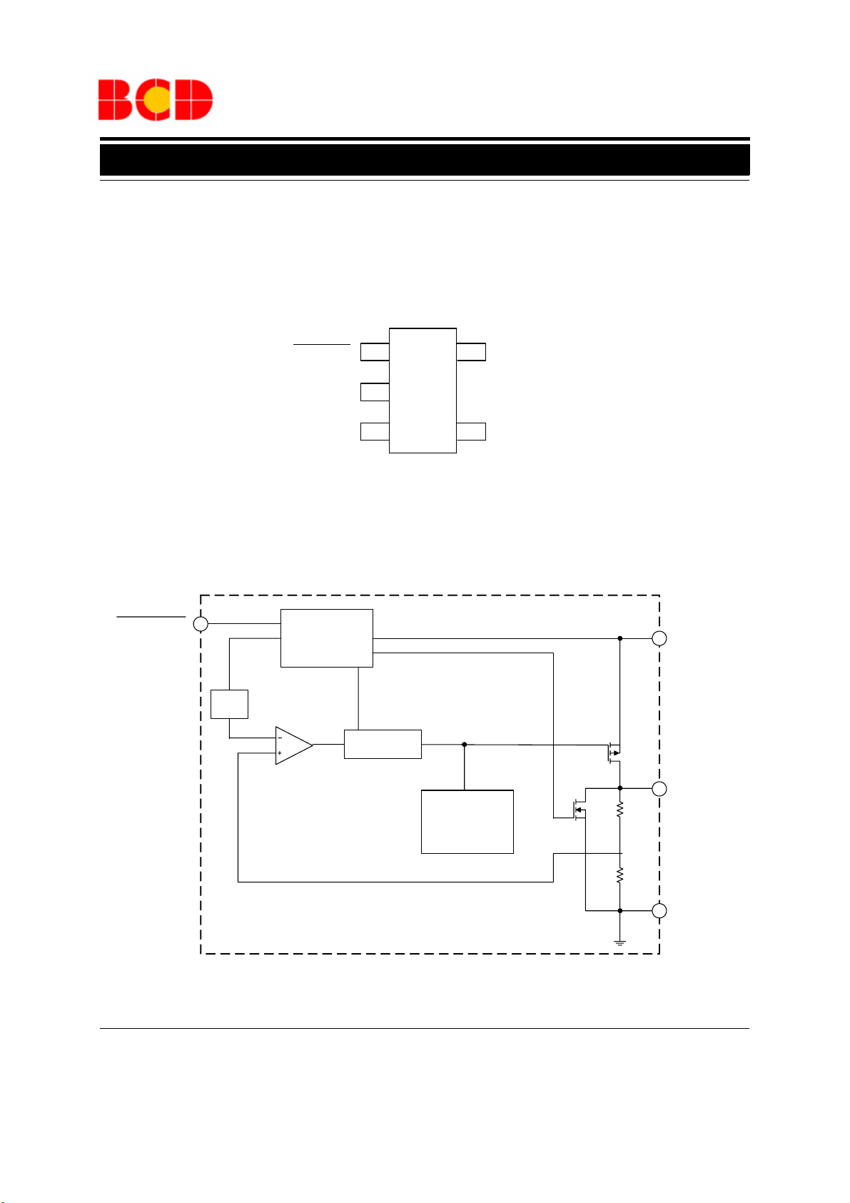
SOT-23-5
Figure 1. Package Type of AP2128
Sept. 2010 Rev. 2.0 BCD Semiconductor Manufacturing Limited
1
Page 2
Data Sheet
300mA HIGH SPEED, EXTREMELY LOW NOISE CMOS LDO REGULATOR AP2128
Pin Configuration
K Package
(SOT-23-5)
Shutdown
Figure 2. Pin Configuration of AP2128 (Top View)
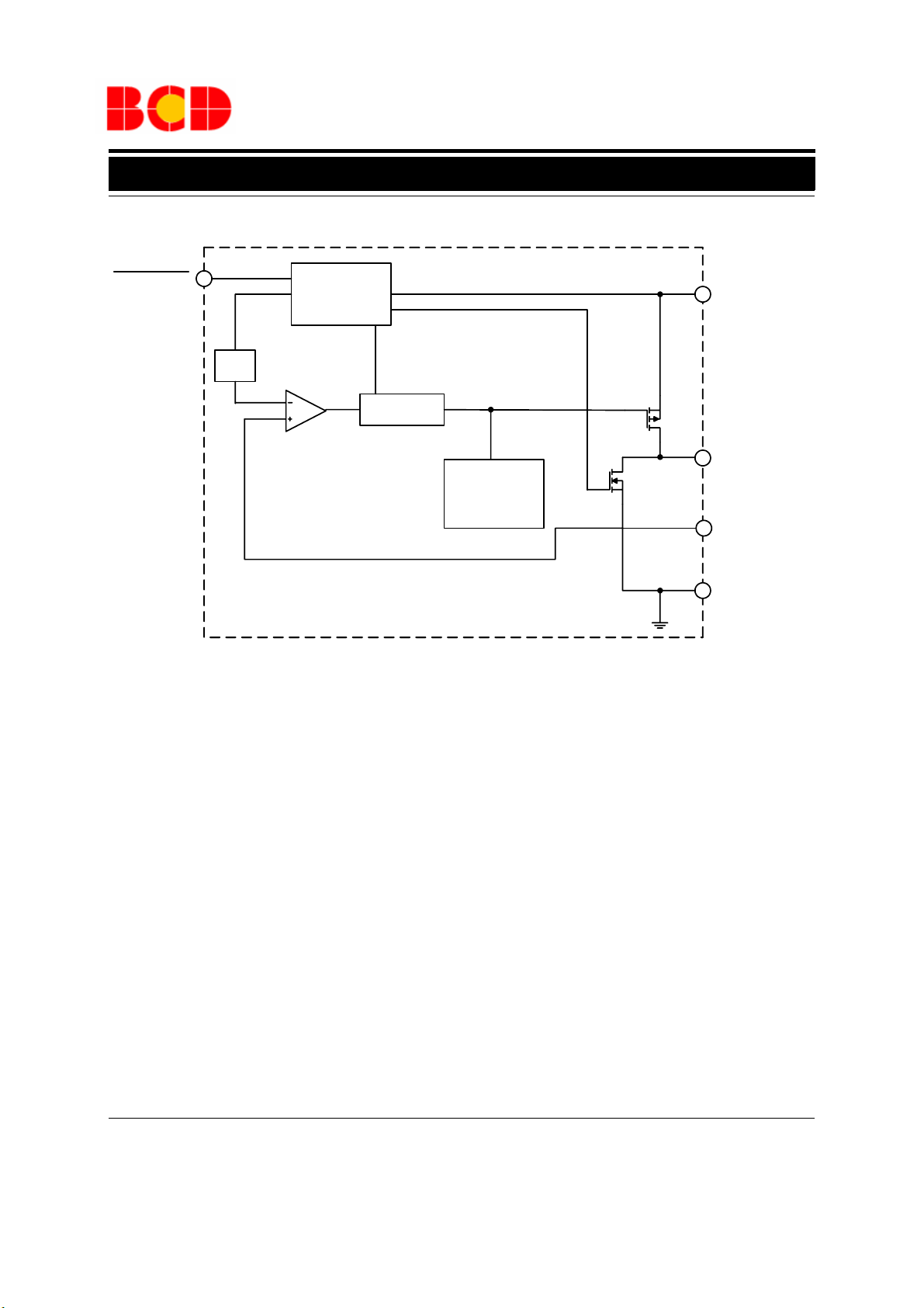
Functional Block Diagram
SHUTDOWN
1
Logic Control
V
REF
GND
V
IN
Shutdown
and
ADJ/NC
1
2
34
MOS Driver
5
V
OUT
3
VIN
4
Current Limint
And
Thermal
Protection
VOUT
2
GND
Fixed Version
Sept. 2010 Rev. 2.0 BCD Semiconductor Manufacturing Limited
2
Page 3
Data Sheet
300mA HIGH SPEED, EXTREMELY LOW NOISE CMOS LDO REGULATOR AP2128
Functional Block Diagram (Continued)
SHUTDOWN
1
V
REF
Shutdown
and
Logic Control
MOS Driver
Current Limint
And
Thermal
Protection
3
VIN
4
VOUT
5
ADJ
2
GND
Adjustable Version
Figure 3. Functional Block Diagram of AP2128
Sept. 2010 Rev. 2.0 BCD Semiconductor Manufacturing Limited
3
Page 4
Data Sheet
300mA HIGH SPEED, EXTREMELY LOW NOISE CMOS LDO REGULATOR AP2128
Ordering Information
AP2128 -
Circuit Type
Package
K: SOT-23-5
Product Package
Temperature
Range
G1: Green
TR: Tape and Reel
ADJ: ADJ Output
1.0: Fixed Output 1.0V
1.2: Fixed Output 1.2V
1.5: Fixed Output 1.5V
1.8: Fixed Output 1.8V
2.5: Fixed Output 2.5V
2.8: Fixed Output 2.8V
3.0: Fixed Output 3.0V
3.3: Fixed Output 3.3V
3.9: Fixed Output 3.9V
4.2: Fixed Output 4.2V
4.75: Fixed Output 4.75V
5.2: Fixed Output 5.2V
Part Number Marking ID Packing Type
AP2128K- ADJTRG1
AP2128K-1.0TRG1 FAJ Tape & Reel
AP2128K-1.2TRG1 FAK Tape & Reel
FAD Tape & Reel
AP2128K-1.5TRG1 GAN Tape & Reel
AP2128K-1.8TRG1 GAP Tape & Reel
AP2128K-2.5TRG1 GAQ Tape & Reel
AP2128 SOT-23-5
BCD Semiconductor's products, as designated with "G1" suffix in the part number, are RoHS compliant and Green.
-40 to 85oC
AP2128K-2.8TRG1 GAR Tape & Reel
AP2128K-3.0TRG1
AP2128K-3.3TRG1 FAL
AP2128K-3.9TRG1 GBU Tape & Reel
AP2128K-4.2TRG1 GAZ Tape & Reel
AP2128K-4.75TRG1 GFZ Tape & Reel
AP2128K-5.2TRG1 GAV Tape & Reel
GAW Tape & Reel
Tap e & Ree l
Sept. 2010 Rev. 2.0 BCD Semiconductor Manufacturing Limited
4
Page 5
Data Sheet
300mA HIGH SPEED, EXTREMELY LOW NOISE CMOS LDO REGULATOR AP2128
Absolute Maximum Ratings (Note 1)
Parameter Symbol Value Unit
Input Voltage V
Shutdown Input Voltage V
Output Current I
Junction Temperature T
Storage Temperature Range T
Lead Temperature (Soldering, 10sec) T
LEAD
Thermal Resistance θ
IN
CE
OUT
J
STG
JA
6.5 V
-0.3 to VIN+0.3 V
450 mA
o
C/W
o
o
o
150
-65 to 150
260
250
C
C
C
ESD (Human Body Model) ESD 6000 V
ESD (Machine Model) ESD 200 V
Note 1: Stresses greater than those listed under "Absolute Maximum Ratings" may cause permanent damage to the device.
These are stress ratings only, and functional operation of the device at these or any other conditions beyond those indicated
under "Recommended Operating Conditions" is not implied. Exposure to "Absolute Maximum Ratings" for extended periods
may affect device reliability.
Recommended Operating Conditions
Parameter Symbol Min Max Unit
Input Voltage V
Operating Ambient Temperature Range T
IN
A
Sept. 2010 Rev. 2.0 BCD Semiconductor Manufacturing Limited
5
2.5 6 V
-40 85
o
C
Page 6
Data Sheet
300mA HIGH SPEED, EXTREMELY LOW NOISE CMOS LDO REGULATOR AP2128
Electrical Characteristics
(AP2128-ADJ, V
min=2.5V, CIN=1µF, C
IN
OUT
=1µF,
Bold typeface applies over -40oC≤TA≤
85oC,
unless otherwise specified.)
Parameter Symbol Conditions Min Typ Max Unit
OUT
VIN=2.5V
1mA≤I
VIN=2.5V,
V
OUT
VIN=2.5V
V
IN
)
1mA≤I
V
IN
)
I
OUT
VIN=2.5V, I
VIN=2.5V,
V
SHUTDOWN
≤300mA
OUT
=98%×V
=2.5V,
≤300mA
OUT
=2.5V to 6V
=30mA
OUT
in off mode
0.784 0.8 0.816 V
2.5 6 V
300 400 mA
OUT
450 mA
0.6 %/A
0.06 %/V
=0mA 60 90 µA
0.1 1.0 µA
Reference Voltage
V
Input Voltage V
Maximum Output Current
Current Limit
Load Regulation
Line Regulation
I
OUT(MAX)
I
LIMIT
∆V
/(∆I
OUT*VOUT
∆V
/(∆VIN*V
Quiescent Current I
Standby Current
I
REF
IN
OUT
OUT
Q
STD
f=100Hz 68 dB
Power Supply
Rejection Ratio
PSRR
Ripple 1Vp-p
=3V
V
IN
f=1KHz 68 dB
f=10KHz 54 dB
UP
)
I
OUT
V
=30mA,
OUT
-40oC≤TA≤
=0V 50 mA
TA=25oC, 10Hz ≤f≤100kHz,
=0.8V
V
OUT
85oC
±100
ppm/
50 µs
60
µVrm s
Output Voltage
(∆V
OUT/VOUT
Temperature Coefficient
Short Current Limit I
Soft Start Time t
RMS Output Noise
Shutdown
"High" Voltage Shutdown input voltage "High" 1.5 6 V
V
/∆T
SHORT
NOISE
o
C
Shutdown
V
R
Shutdown
tance
Thermal Shutdown 165
Thermal Shutdown Hysteresis 30
Thermal Resistance
"Low" Voltage Shutdown input voltage "Low" 0 0.4 V
Discharge MOSFET
OUT
DS(ON)
Pull Down Resis-
θ
JC
Shutdown input voltage "Low" 60 Ω
3MΩ
SOT-23-5 150
o
C/W
o
C
o
C
Sept. 2010 Rev. 2.0 BCD Semiconductor Manufacturing Limited
6
Page 7

Data Sheet
300mA HIGH SPEED, EXTREMELY LOW NOISE CMOS LDO REGULATOR AP2128
Electrical Characteristics (Continued)
(AP2128-1.0V/1.2V/1.5V/1.8V, VINmin.=2.5V, CIN=1µF, C
erwise specified.)
Parameter Symbol Conditions Min Typ Max Unit
Output Voltage
V
Input Voltage V
Maximum Output Current
Current Limit
Load Regulation
Line Regulation
Dropout Voltage
I
OUT(MAX)
I
LIMIT
∆V
/(∆I
OUT*VOUT
∆V
/(∆VIN*V
V
Quiescent Current I
(∆V
OUT/VOUT
I
PSRR
Standby Current
Power Supply
Rejection Ratio
Output Voltage
Temperature Coefficient
Short Current Limit I
SHORT
Soft Start Time t
Shutdown
"High" Voltage Shutdown input voltage "High" 1.5 6 V
OUT
IN
OUT
OUT
OUT
DROP
Q
STD
/∆T
UP
VIN=2.5V
1mA≤I
VIN=2.5V,
V
OUT
VIN=2.5V
V
IN
)
1mA≤I
V
IN
)
I
OUT
V
OUT
V
OUT
V
OUT
V
OUT
VIN=2.5V, I
VIN=2.5V,
V
SHUTDOWN
Ripple 1Vp-p
V
IN
)
I
OUT
V
OUT
=1µF,
OUT
OUT
Bold typeface applies over -40oC≤TA≤
98%×
≤300mA
V
OUT
85oC,
unless oth-
102%×
V
OUT
2.5 6 V
=98%×V
OUT
300 400 mA
450 mA
=2.5V,
≤300mA
OUT
=2.5V to 6V
=30mA
=1.0V, I
OUT
=1.2V, I
OUT
=1.5V, I
OUT
=1.8V, I
OUT
OUT
in off mode
=300mA 1400 1500
=300mA 1200 1300
=300mA 900 1000
=300mA 600 700
=0mA 60 90 µA
0.1 1.0 µA
0.6 %/A
0.06 %/V
f=100Hz 68 dB
=3V
f=1KHz 68 dB
f=10KHz 54 dB
=30mA,
-40oC≤TA≤
85oC
±100
=0V 50 mA
50 µs
V
mV
ppm/
o
C
Shutdown
V
R
Shutdown Pull Down Resistance
Thermal Shutdown 165
Thermal Shutdown Hysteresis 30
Thermal Resistance
"Low" Voltage Shutdown input voltage "Low" 0 0.4 V
Discharge MOSFET
OUT
DS(ON)
Shutdown input voltage "Low" 60 Ω
3MΩ
θ
JC
SOT-23-5 150
o
o
o
C/W
C
C
Sept. 2010 Rev. 2.0 BCD Semiconductor Manufacturing Limited
7
Page 8

Data Sheet
300mA HIGH SPEED, EXTREMELY LOW NOISE CMOS LDO REGULATOR AP2128
Electrical Characteristics (Continued)
(AP2128-2.5V/2.8V/3.0V/3.3V/3.9V/4.2V/4.75V, VIN=V
face applies over
-40oC≤TA≤
85oC,
unless otherwise specified.)
+1V; AP2128-5.2V, VIN=6V, CIN=1µF, C
OUT
OUT
=1µF,
Bold type-
Parameter Symbol Conditions Min Typ Max Unit
Output Voltage
V
Input Voltage V
Maximum Output Current
Current Limit
Load Regulation
Line Regulation
Dropout Voltage
I
OUT(MAX)
I
LIMIT
∆V
/(∆I
OUT*VOUT
∆V
/(∆VIN*V
V
Quiescent Current I
(∆V
OUT/VOUT
I
PSRR
Standby Current
Power Supply
Rejection Ratio
Output Voltage
Temperature Coefficient
Short Current Limit I
SHORT
OUT
IN
OUT
OUT
DROP
Q
STD
/∆T
OUT
)
)
)
VIN=V
1mA≤I
VIN-V
V
OUT
VIN-V
V
IN-VOUT
1mA≤I
V
OUT
I
OUT
V
OUT
3.9V, 4.2V, I
V
OUT
I
OUT
VIN=V
VIN=V
V
SHUTDOWN
AP2128-2.5V to
4.2V, Ripple
1Vp-p
V
IN=VOUT
AP2128-4.75V ,
Ripple 0.5Vp-p
V
IN=VOUT
AP2128-5.2V ,
Ripple 0.5Vp-p
V
IN
I
OUT
V
OUT
OUT
OUT
+1V
≤300mA
98%×
V
OUT
102%×
V
OUT
2.5 6 V
=1V,
OUT
=98%×V
OUT
OUT
=1V
=1V,
≤300mA
OUT
+0.5V≤VIN≤6V,
=30mA
=2.5V, 2.8V, 3.0V, 3.3V,
=300mA
OUT
=4.75V and 5.2V,
=300mA
OUT
OUT
+1V, I
+1V,
=0mA 60 90 µA
OUT
in off mode
300 400 mA
450 mA
0.6 %/A
0.06 %/V
170 300
140 300
0.1 1.0 µA
f=100Hz 68
f=1KHz 68
+1V
f=10KHz 54
f=100Hz 63
f=1KHz 63
+1V
f=10KHz 45
f=100Hz 63
f=1KHz 63
=6V
=30mA,
f=10KHz 45
-40oC≤TA≤
85oC
±100
=0V 50 mA
ppm/
V
mV
dB
o
C
Sept. 2010 Rev. 2.0 BCD Semiconductor Manufacturing Limited
8
Page 9

Data Sheet
300mA HIGH SPEED, EXTREMELY LOW NOISE CMOS LDO REGULATOR AP2128
Electrical Characteristics (Continued)
(AP2128-2.5V/2.8V/3.0V/3.3V/3.9V/4.2V/4.75V, VIN=V
face applies over
-40oC≤TA≤
85oC,
unless otherwise specified.)
Parameter Symbol Conditions Min Typ Max Unit
Soft Start Time t
Shutdown
"High" Voltage Shutdown input voltage "High" 1.5 6 V
UP
+1V; AP2128-5.2V, VIN=6V, CIN=1µF, C
OUT
=1µF,
OUT
Bold type-
50 µs
Shutdown
V
R
DS(ON)
Shutdown
tance
"Low" Voltage Shutdown input voltage "Low" 0 0.4 V
Discharge MOSFET
OUT
Pull Down Resis-
Shutdown input voltage "Low" 60 Ω
3MΩ
Thermal Shutdown 165
Thermal Shutdown Hysteresis 30
Thermal Resistance
θ
JC
SOT-23-5 150
o
C/W
o
C
o
C
Sept. 2010 Rev. 2.0 BCD Semiconductor Manufacturing Limited
9
Page 10

Data Sheet
300mA HIGH SPEED, EXTREMELY LOW NOISE CMOS LDO REGULATOR AP2128
Typical Performance Characteristics
1.0
3.5
0.9
0.8
3.0
0.7
2.5
0.6
2.0
0.5
0.4
1.5
0.3
Output Voltge (V)
Output Voltage (V)
1.0
0.2
0.5
0.1
0.0
0.0
0 100 200 300 400 500
0 50 100 150 200 250 300 350 400 450 500
VIN=2.5V, V
Output Current (V)
Output Current (mA)
Tc=-40oC
Tc=25oC
Tc=85oC
V
=4.4V
IN
OUT
TC=-40oC
TC=25oC
TC=125oC
=0.8V
Figure 4. Output Voltage vs. Output Current
3.5
3.0
2.5
2.0
1.5
=250C, V
T
C
VIN=3.8V
VIN=4.3V
VIN=6V
OUT
=3.3V
Output Voltage (V)
1.0
0.5
0.0
0.00.10.20.30.40.5
Output Current (A)
3.5
3.0
2.5
2.0
1.5
=4.3V, V
V
IN
TC=-40oC
TC=25oC
TC=85oC
Output Voltage (V)
1.0
0.5
0.0
0.0 0.1 0.2 0.3 0.4 0.5
Output Current (A)
Figure 5. Output Voltage vs. Output Current
6.0
5.5
5.0
4.5
4.0
3.5
3.0
2.5
2.0
Output Voltage (V)
1.5
1.0
0.5
0.0
0.0 0.1 0.2 0.3 0.4 0.5
Output Current (A)
V
=6V, V
IN
OUT
TC=-40oC
TC=25oC
TC=85oC
OUT
=3.3V
=5.2V
Figure 6. Output Voltage vs. Output Current Figure 7. Output Voltage vs. Output Current
Sept. 2010 Rev. 2.0 BCD Semiconductor Manufacturing Limited
10
Page 11

Data Sheet
300mA HIGH SPEED, EXTREMELY LOW NOISE CMOS LDO REGULATOR AP2128
Typical Performance Characteristics (Continued)
240
220
200
180
160
140
120
100
Dropout Voltage (mV)
TC=-40oC
TC=25oC
TC=85oC
V
=3.3V
OUT
80
60
40
20
0
50 100 150 200 250 300
Output Current (mA)
Figure 8. Dropout Voltage vs. Output Current
0.20
0.18
0.16
0.14
0.12
0.10
0.08
0.06
Dropout Voltage (V)
0.04
0.02
0.00
-40-200 20406080
Case Temperature (oC)
I
=10mA
OUT
I
=150mA
OUT
I
=300mA
OUT
=4.3V, V
V
IN
OUT
=3.3V
180
160
140
120
100
80
60
Dropout Voltage (mV)
40
20
TC=-40oC
TC=25oC
TC=85oC
=6V, V
OUT
=5.2V
V
IN
0
0.00 0.05 0.10 0.15 0.20 0.25 0.30
Output Current (A)
Figure 9. Dropout Voltage vs. Output Current
160
150
140
130
120
110
100
90
80
70
60
50
Dropout Voltage (mV)
40
30
20
10
0
-40-200 20406080
Case Temperature (oC)
V
=6V, V
IN
I
OUT
I
OUT
I
OUT
=10mA
=150mA
=300mA
=5.2V
OUT
Figure 10. Dropout Voltage vs. Case Temperature
Figure 11. Dropout Voltage vs. Case Temperature
Sept. 2010 Rev. 2.0 BCD Semiconductor Manufacturing Limited
11
Page 12

Data Sheet
300mA HIGH SPEED, EXTREMELY LOW NOISE CMOS LDO REGULATOR AP2128
Typical Performance Characteristics (Continued)
120
115
110
105
100
95
90
85
80
75
70
Quiescent Current (µA)
65
60
55
50
TC=-40oC
TC=25oC
TC=85oC
V
=2.5V, V
IN
0 50 100 150 200 250 300
OUT
=0.8V
Output Current (mA)
Figure 12. Quiescent Current vs. Output Current
115
110
105
100
Quiescent Current (µA)
TC=-40oC
TC=25oC
TC=85oC
=6V, V
OUT
=5.2V
V
IN
95
90
85
80
75
0.00 0.05 0.10 0.15 0.20 0.25 0.30
Output Current (A)
115
110
105
100
95
90
85
80
75
Quiescent Current (µA)
70
65
TC=-40oC
TC=25oC
TC=85oC
=4.3V, V
V
IN
0 50 100 150 200 250 300
OUT
=3.3V
Output Current (mA)
Figure 13. Quiescent Current vs. Output Current
70
68
66
64
62
60
58
56
Quiescent Current (µA)
54
52
50
-40-20 0 20406080100120
Case Temperature (oC)
I
OUT
V
=0
=2.5V, V
IN
OUT
=0.8V
Figure 14. Quiescent Current vs. Output Current
Figure 15. Quiescent Current vs. Case Temperature
Sept. 2010 Rev. 2.0 BCD Semiconductor Manufacturing Limited
12
Page 13

Data Sheet
300mA HIGH SPEED, EXTREMELY LOW NOISE CMOS LDO REGULATOR AP2128
Typical Performance Characteristics (Continued)
71
70
69
68
67
66
65
Quiescent Current (µA)
64
63
62
-40-20 0 20406080100120
=4.3V, V
V
IN
I
=0
OUT
=3.3V
OUT
Case Temperature (oC)
74
72
70
68
66
64
Quiescent Current (µA)
62
60
-40-20 0 20406080100120
Case Temperature (oC)
I
=0
OUT
=6V, V
OUT
=5.2V
V
IN
Figure 16. Quiescent Current vs. Case Temperature Figure 17. Quiescent Current vs. Case Temperature
80
70
60
50
40
30
Quiescent Current (µA)
20
10
0
1.0 1.5 2.0 2.5 3.0 3.5 4.0 4.5 5.0 5.5 6.0
TC=25oC
=0, V
OUT
=0.8V
I
OUT
Input Voltage (V)
80
70
60
50
40
30
20
Quiescent Current (µA)
10
0
0123456
Input Voltage (V)
I
OUT
TC=25oC
=0, V
OUT
=3.3V
Figure 18. Quiescent Current vs. Input Voltage
Figure 19. Quiescent Current vs. Input Voltage
Sept. 2010 Rev. 2.0 BCD Semiconductor Manufacturing Limited
13
Page 14

Data Sheet
300mA HIGH SPEED, EXTREMELY LOW NOISE CMOS LDO REGULATOR AP2128
Typical Performance Characteristics (Continued)
80
TC=25oC
=0, V
OUT
=5.2V
I
70
OUT
60
50
40
30
Quiescent Current (µA)
20
10
0
0123456
Input Voltage (V)
0.807
0.806
0.805
0.804
0.803
Output Voltage (V)
0.802
0.801
-40-20 0 20406080100120
Case Temperature (oC)
VIN=2.5V, CIN=C
=10mA, V
I
OUT
Figure 20. Quiescent Current vs. Input Voltage Figure 21. Output Voltage vs. Case Temperature
3.348
3.346
3.344
3.342
3.340
3.338
3.336
3.334
3.332
Output Voltage (V)
3.330
3.328
3.326
-40 -20 0 20 40 60 80 100 120
=4.3V, V
V
IN
I
OUT
Case Temperature (oC)
=10mA
OUT
=3.3V
5.250
5.245
5.240
5.235
5.230
5.225
5.220
5.215
Output Voltage (V)
5.210
5.205
5.200
5.195
-40-20 0 20406080100120
Case Temperature (oC)
V
OUT
=6V, V
IN
OUT
=0.8V
I
OUT
=1µF
=10mA
OUT
=5.2V
Figure 22. Output Voltage vs. Case Temperature Figure 23. Output Voltage vs. Case Temperature
Sept. 2010 Rev. 2.0 BCD Semiconductor Manufacturing Limited
14
Page 15

Data Sheet
300mA HIGH SPEED, EXTREMELY LOW NOISE CMOS LDO REGULATOR AP2128
Typical Performance Characteristics (Continued)
VIN=2.5V, V
34
32
30
28
Short Current (mA)
26
-40-20 0 20406080100120
=0.8V, CIN=C
OUT
=1µF
OUT
Case Temperature (oC)
1.0
0.9
0.8
0.7
0.6
0.5
0.4
0.3
Output Voltge (V)
0.2
0.1
0.0
012345678
V
OUT
TC=-40oC
TC=25oC
TC=85oC
=0.8V
Input Voltage (V)
56
VIN=6V, V
54
52
50
48
46
44
42
40
38
Short Current (mA)
36
34
32
30
-40-20 0 20406080100120
OUT
=5.2V
Case Temperature (oC)
Figure 25. Short Current vs. Case TemperatureFigure 24. Short Current vs. Case Temperature
1.0
0.9
0.8
0.7
0.6
0.5
0.4
Output Voltge (V)
0.3
0.2
0.1
0.0
0123456
Input Voltage (V)
V
TC=-40oC
TC=25oC
TC=85oC
=0.8V
OUT
Figure 26. Output Voltage vs. Input Voltage (I
=0mA) Figure 27. Output Voltage vs. Input Voltage (I
OUT
OUT
=300mA)
Sept. 2010 Rev. 2.0 BCD Semiconductor Manufacturing Limited
15
Page 16

Data Sheet
300mA HIGH SPEED, EXTREMELY LOW NOISE CMOS LDO REGULATOR AP2128
Typical Performance Characteristics (Continued)
Output Voltage (V)
3.5
3.0
2.5
2.0
1.5
1.0
0.5
0.0
TC=-40oC
TC=25oC
TC=85oC
=0, V
OUT
=3.3V
Input Voltage (V)
I
OUT
0.0 0.5 1.0 1.5 2.0 2.5 3.0 3.5
Figure 28. Output Voltage vs. Input Voltage
2.0
1.8
1.6
1.4
1.2
1.0
0.8
0.6
Power Dissipation (W)
0.4
0.2
0.0
-40 -20 0 20 40 60 80 100 120
Case Temperature (oC)
V
=0.8V
OUT
No heatsink
6
TC=-40oC
5
TC=25oC
TC=85oC
4
=0, V
OUT
=5.2V
I
OUT
3
2
Output Voltage (V)
1
0
0123456
Input Voltage (V)
Figure 29. Output Voltage vs. Input Voltage
I
OUT
V
OUT
Figure 30. Power Dissipation vs. Case Temperature
(Conditions: C
I
Figure 31. Load Transient
IN=COUT
OUT
=1µF, VIN=2.5V, V
=10mA to 300mA)
OUT
=0.8V,
Sept. 2010 Rev. 2.0 BCD Semiconductor Manufacturing Limited
16
Page 17

Data Sheet
300mA HIGH SPEED, EXTREMELY LOW NOISE CMOS LDO REGULATOR AP2128
Typical Performance Characteristics (Continued)
I
OUT
V
OUT
(Conditions: C
I
V
IN
Figure 32. Load Transient
IN=COUT
OUT
=1µF, VIN=4.4V, V
=10mA to 300mA)
OUT
=3.3V
V
V
IN
OUT
V
(Conditions: I
OUT
Figure 33. Line Transient
=30mA, CIN=C
OUT
=2.5 to 3.5V, V
V
IN
OUT
OUT
=0.8V)
=1µF,
V
V
OUT
Figure 34. Line Transient
(Conditions: I
V
IN
=30mA, CIN=C
OUT
=4 to 5V, V
OUT
=3.3V)
OUT
=1µF,
Shutdown
Figure 35. Soft Start Time
(Conditions: I
V
Shutdown
=0mA, CIN=C
OUT
=0 to 2V, V
OUT
OUT
=3.3V)
=1µF,
Sept. 2010 Rev. 2.0 BCD Semiconductor Manufacturing Limited
17
Page 18

Data Sheet
300mA HIGH SPEED, EXTREMELY LOW NOISE CMOS LDO REGULATOR AP2128
Typical Performance Characteristics (Continued)
V
V
Shutdown
OUT
100
PSRR (dB)
Figure 36. Soft Start Time
(Conditions: I
V
Shutdown
90
80
70
60
50
40
30
20
10
0
100 1000 10000 100000
=0mA, CIN=C
OUT
=0 to 2V, V
I
I
ripple=1Vpp, C
Frequency (Hz)
OUT
OUT
OUT
=10mA
=300mA
=0.8V)
=1µF, V
OUT
OUT
=1µF,
=3.3V
OUT
100
90
80
70
60
50
40
PSRR (dB)
30
20
10
0
100 1000 10000 100000
I
=10mA
OUT
I
=300mA
OUT
ripple=1Vpp, C
OUT
=1µF, V
OUT
=0.8V
Frequency (Hz)
Figure 37. PSRR vs. Frequency
70
60
50
PSRR (dB)
40
30
I
=10mA
20
10
OUT
I
=300mA
OUT
V
OUT
=5.2V, C
=1µF, ripple=0.5Vpp
OUT
100 1k 10k 100k
Frequency (Hz)
Figure 38. PSRR vs. Frequency
Figure 39. PSRR vs. Frequency
Sept. 2010 Rev. 2.0 BCD Semiconductor Manufacturing Limited
18
Page 19

Data Sheet
300mA HIGH SPEED, EXTREMELY LOW NOISE CMOS LDO REGULATOR AP2128
Typical Application
V
IN
V
=0.8(1+R1/R2) V
OUT
V
IN
C
IN
1µF
V
V
IN
IN
AP2128
GND
V
OUT
V
OUT
R1
ADJShutdown
C
OUT
1µF
R2
V
OUT
V
OUT
AP2128
Shutdown
C
=1.0V to 5.2V
V
OUT
IN
1µF
Figure 40. Typical Application of AP2128
GND
Sept. 2010 Rev. 2.0 BCD Semiconductor Manufacturing Limited
19
C
OUT
1µF
Page 20
Data Sheet
300mA HIGH SPEED, EXTREMELY LOW NOISE CMOS LDO REGULATOR AP2128
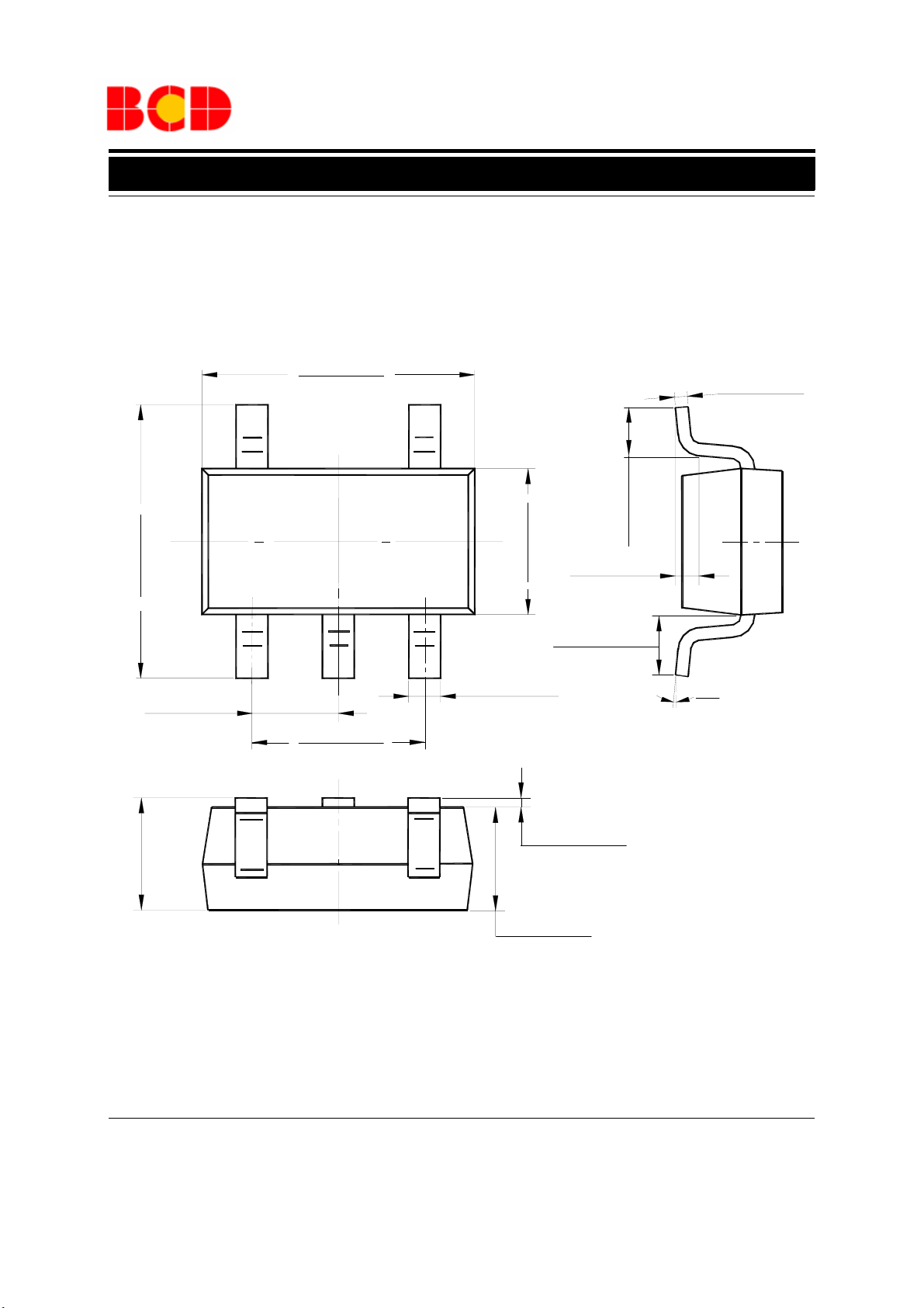
Mechanical Dimensions
SOT-23-5 Unit: mm(inch)
2.820(0.111)
3.020(0.119)
)
)
4
2
2
1
0
0
.
.
0
)
)
7
)
)
4
6
0
1
1
1
.
.
0
0
(
(
0
0
5
5
6
9
.
.
2
2
9
6
5
0
0
.
.
0
0
(
(
0
0
0
0
5
7
.
.
1
1
0.200(0.008)
0
(
(
0
0
0
0
3
6
.
.
0
0
0.100(0.004)
0.200(0.008)
0.950(0.037)
P
Y
T
)
7
5
0
.
X
0
A
(
0
M
5
4
.
1
1.800(0.071)
2.000(0.079)
0.300(0.012)
0.400(0.016)
0
0
0
0
0
9
.
.
1
0
0
3
0
0
7
.
0
R
0
(
0
0
0
.
0
(
0
5
1
.
5
3
0
.
0
(
)
)
.
0
1
0
5
(
)
8
2
0
.
0
(
F
E
0°
8°
)
.
0
0
0
)
.
0
6
0
Sept. 2010 Rev. 2.0 BCD Semiconductor Manufacturing Limited
20
Page 21

BCD Semiconductor Manufacturing Limited
IMPORTANT NOTICE
IMPORTANT NOTICE
BCD Semiconductor Manufacturing Limited reserves the right to make changes without further notice to any products or specifi-
BCD Semiconductor Manufacturing Limited reserves the right to make changes without further notice to any products or specifi-
cations herein. BCD Semiconductor Manufacturing Limited does not assume any responsibility for use of any its products for any
cations herein. BCD Semiconductor Manufacturing Limited does not assume any responsibility for use of any its products for any
particular purpose, nor does BCD Semiconductor Manufacturing Limited assume any liability arising out of the application or use
particular purpose, nor does BCD Semiconductor Manufacturing Limited assume any liability arising out of the application or use
of any its products or circuits. BCD Semiconductor Manufacturing Limited does not convey any license under its patent rights or
of any its products or circuits. BCD Semiconductor Manufacturing Limited does not convey any license under its patent rights or
other rights nor the rights of others.
other rights nor the rights of others.
http://www.bcdsemi.com
MAIN SITE
MAIN SITE
- Headquarters
BCD Semiconductor Manufacturing Limited
BCD Semiconductor Manufactur ing Limited
- Wafer Fab
No. 1600, Zi Xing Road, Shanghai ZiZhu Science-based Industrial Park, 200241, China
Shanghai SIM-BCD Semiconductor Manufacturing Limited
Tel: +86-21-24162266, Fax: +86-21-24162277
800, Yi Shan Road, Shanghai 200233, China
Tel: +86-21-6485 1491, Fax: +86-21-5450 0008
REGIONAL SALES OFFICE
Shenzhen Office
REGIONAL SALES OFFICE
Shanghai SIM-BCD Semiconductor Manufacturing Co., Ltd., Shenzhen Office
Shenzhen Office
Unit A Room 1203, Skyworth Bldg., Gaoxin Ave.1.S., Nanshan District, Shenzhen,
Shanghai SIM-BCD Semiconductor Manufacturing Co., Ltd. Shenzhen Office
China
Advanced Analog Circuits (Shanghai) Corporation Shenzhen Office
Tel: +86-755-8826 7951
Room E, 5F, Noble Center, No.1006, 3rd Fuzhong Road, Futian District, Shenzhen 518026, China
Fax: +86-755-8826 7865
Tel: +86-755-8826 7951
Fax: +86-755-8826 7865
- Wafer Fab
BCD Semiconductor Manufacturing Limited
Shanghai SIM-BCD Semiconductor Manufacturing Co., Ltd.
- IC Design Group
800 Yi Shan Road, Shanghai 200233, China
Advanced Analog Circuits (Shanghai) Corporation
Tel: +86-21-6485 1491, Fax: +86-21-5450 0008
8F, Zone B, 900, Yi Shan Road, Shanghai 200233, China
Tel: +86-21-6495 9539, Fax: +86-21-6485 9673
Taiwan Office
BCD Semiconductor (Taiwan) Company Limited
Taiwan Office
4F, 298-1, Rui Guang Road, Nei-Hu District, Taipei,
BCD Semiconductor (Taiwan) Company Limited
Tai wan
4F, 298-1, Rui Guang Road, Nei-Hu District, Taipei,
Tel: +886-2-2656 2808
Taiwan
Fax: +886-2-2656 2806
Tel: +886-2-2656 2808
Fax: +886-2-2656 2806
USA Office
BCD Semiconductor Corp.
USA Office
30920 Huntwood Ave. Hayward,
BCD Semiconductor Corporation
CA 94544, USA
30920 Huntwood Ave. Hayward,
Tel : +1-510-324-2988
CA 94544, U.S.A
Fax: +1-510-324-2788
Tel : +1-510-324-2988
Fax: +1-510-324-2788
 Loading...