

Page 1
Data Sheet
300mA HIGH SPEED, EXTREMELY LOW NOISE CMOS LDO REGULATOR AP2125
General Description
The AP2125 series are 300mA, positive voltage regulator ICs fabricated by CMOS process.
Each of these ICs is equipped with a voltage reference,
an error amplifier, a resistor network for setting output
voltage, a chip enable circuit, a current limit circuit and
OTSD (over temperature shut down) circuit to prevent
the IC from over current and over temperature.
The AP2125 series have features of high ripple rejection, low dropout voltage, low noise, high output voltage accuracy and low current consumption which
make them ideal for use in various battery-powered
apparatus.
The AP2125 have 1.8V, 2.5V, 2.8V, 3.0V, 3.3V, 4.15V
and 4.2V fixed voltage versions.
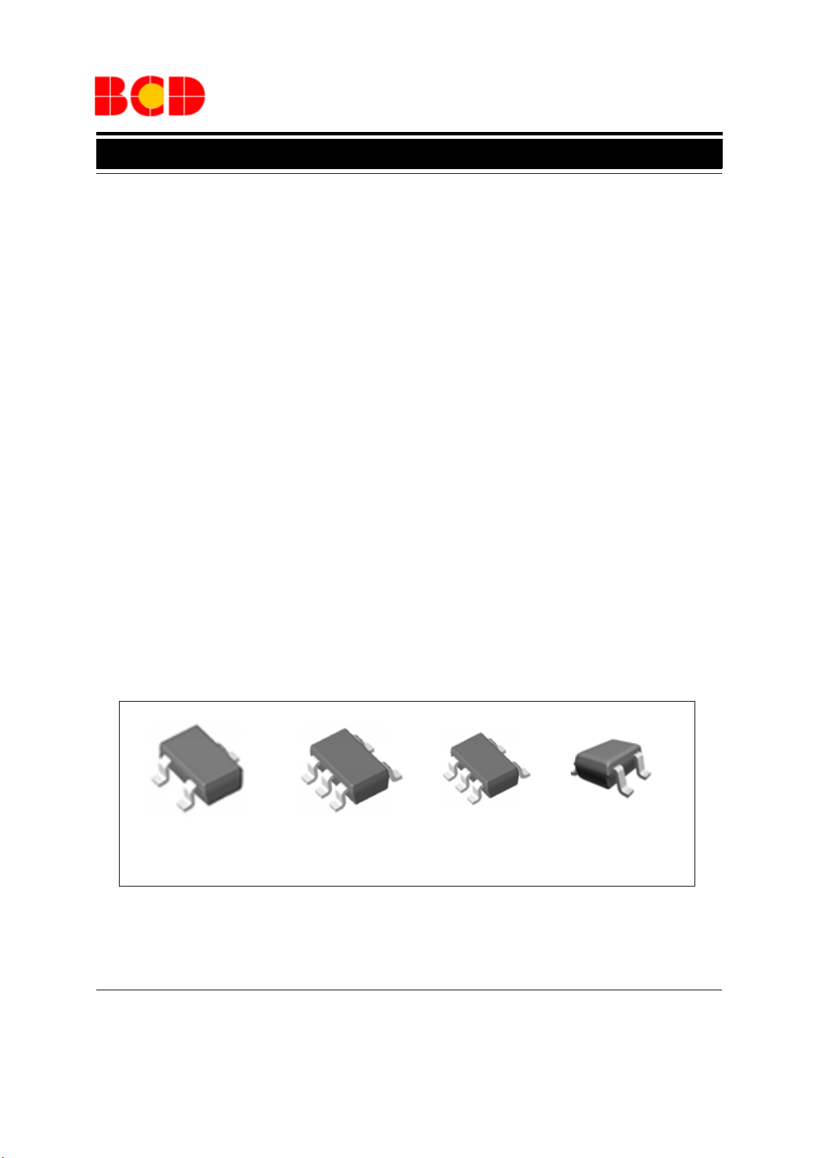
These ICs are available in tiny SC-70-5 and SC-82
packages as well as industry standard SOT-23-3 and
SOT-23-5 packages.
Features
· Excellent Ripple Rejection: 70dB Typical (1.8V
Version)
· Low Dropout Voltage: 65mV (I
3.3V Version)
· Low Standby Current: 0.01µA Typical
· Low Quiescent Current: 60µA Typical
· Extremely Low Noise: 50µVrms Typical
· Maximum Output Current: 300mA (Min.)
· High Output Voltage Accuracy:
· Compatible with Low ESR Ceramic Capacitor
· Excellent Line/Load Regulation
±2%
OUT
=100mA,
Applications
· CDMA/GSM Cellular Handsets
· Battery-powered Equipments
· Laptops, Palmtops, Notebook Computers
· Hand-held Instruments
· PCMCIA Cards
· Portable Information Appliances
SOT-23-3 SOT-23-5 SC-70-5
Figure 1. Package Types of AP2125
BCD Semiconductor Manufacturing LimitedSep. 2012 Rev. 1. 5
1
SC-82
Page 2
Data Sheet
3
2
1
V
IN
GND
V
OUT
1
2
34
5 V
OUT
NC
CE
GND
V
IN
1
2
3
4
CE
GND V
OUT
V
IN
300mA HIGH SPEED, EXTREMELY LOW NOISE CMOS LDO REGULATOR AP2125
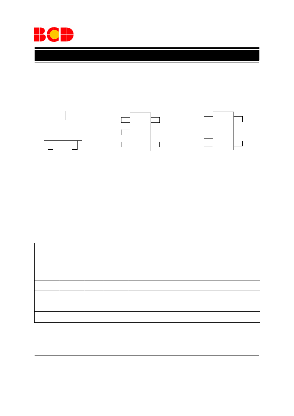
Pin Configuration
N Package
(SOT-23-3)
K/KS Package
KC Package
(SOT-23-5/SC-70-5)
Figure 2. Pin Configuration of AP2125 (Top View)
(SC-82)
Pin Description
Pin Number
Pin Name Function
SOT-23-3 SOT-23-5/
SC-70-5
314V
1 2 2 GND Ground
3 1 CE Active high enable input pin. Logic high=enable, logic low=shutdown
4 NC No connection
253V
SC-82
IN
OUT
Input voltage
Regulated output voltage
BCD Semiconductor Manufacturing LimitedSep. 2012 Rev. 1. 5
2
Page 3
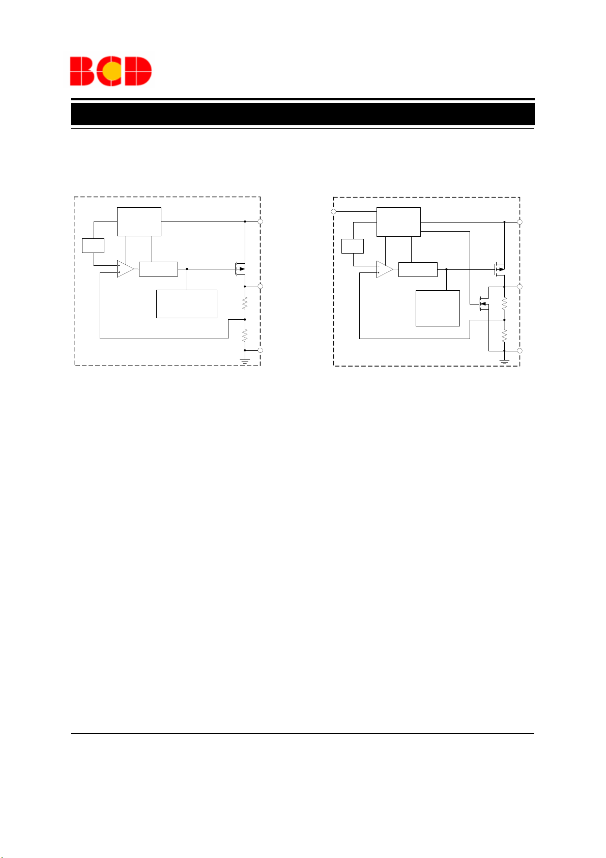
Data Sheet
V
REF
Shutdown
and
Logic Control
MOS Driver
Current Limit
and
Thermal Protection
V
REF
Shutdown
and
Logic Control
MOS Driver
Current Limit
and
Thermal
Protection
300mA HIGH SPEED, EXTREMELY LOW NOISE CMOS LDO REGULATOR AP2125
Functional Block Diagram
3 (1)
3
V
IN
CE
1 (4)
V
IN
SOT-23-3
2
V
OUT
1
GND
A(B)
A SOT-23-5/SC-70-5
B SC-82
Figure 3. Functional Block Diagram of AP2125
5 (3)
2 (2)
V
OUT
GND
BCD Semiconductor Manufacturing LimitedSep. 2012 Rev. 1. 5
3
Page 4
Data Sheet
300mA HIGH SPEED, EXTREMELY LOW NOISE CMOS LDO REGULATOR AP2125
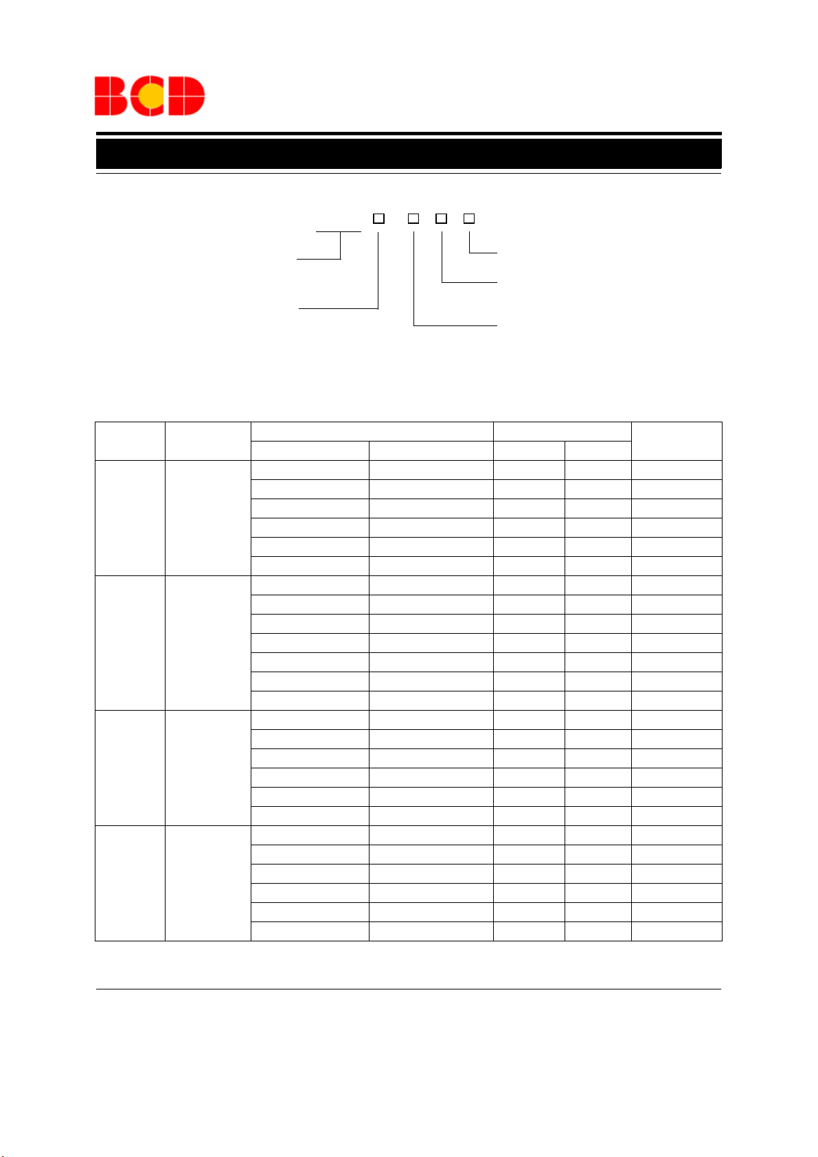
Ordering Information
AP2125 -
Package
SOT-23-3
SOT-23-5
SC-70-5
SC-82
Circuit Type
Package
N: SOT-23-3
K: SOT-23-5
KS: SC-70-5
KC: SC-82
Temperature
Range
o
-40 to 85
-40 to 85
-40 to 85
-40 to 85
C
o
C
o
C
o
C
E1: Lead Free
G1: Green
TR: Tape and Reel
1.8: Fixed Output 1.8V
2.5: Fixed Output 2.5V
2.8: Fixed Output 2.8V
3.0: Fixed Output 3.0V
3.3: Fixed Output 3.3V
4.15: Fixed Output 4.15V
4.2: Fixed Output 4.2V
Part Number Marking ID
Lead Free Green Lead Free Green
AP2125N-1.8TRE1 AP2125N-1.8TRG1 EJ2 GJ2 Tape & Reel
AP2125N-2.5TRE1 AP2125N-2.5TRG1 EJ4 GJ4 Tape & Reel
AP2125N-2.8TRE1 AP2125N-2.8TRG1 EJ5 GJ5 Tape & Reel
AP2125N-3.0TRE1 AP2125N-3.0TRG1 EJ6 GJ6 Tape & Reel
AP2125N-3.3TRE1 AP2125N-3.3TRG1 EJ7 GJ7 Tape & Reel
AP2125N-4.2TRE1 AP2125N-4.2TRG1 EJ3 GJ3 Tape & Reel
AP2125K-1.8TRE1 AP2125K-1.8TRG1 ECB GCB Tape & Reel
AP2125K-2.5TRE1 AP2125K-2.5TRG1 ECD GCD Tape & Reel
AP2125K-2.8TRE1 AP2125K-2.8TRG1 ECE GCE Tape & Reel
AP2125K-3.0TRE1 AP2125K-3.0TRG1 ECF GCF Tape & Reel
AP2125K-3.3TRE1 AP2125K-3.3TRG1 ECG GCG Tape & Reel
AP2125K-4.15TRG1 GCJ Tape & Reel
AP2125K-4.2TRE1 AP2125K-4.2TRG1 ECC GCC Tape & Reel
AP2125KS-1.8TRE1 AP2125KS-1.8TRG1 26 B6 Tape & Reel
AP2125KS-2.5TRE1 AP2125KS-2.5TRG1 35 C5 Tape & Reel
AP2125KS-2.8TRE1 AP2125KS-2.8TRG1 27 B7 Tape & Reel
AP2125KS-3.0TRE1 AP2125KS-3.0TRG1 36 C6 Tape & Reel
AP2125KS-3.3TRE1 AP2125KS-3.3TRG1 28 B8 Tape & Reel
AP2125KS-4.2TRE1 AP2125KS-4.2TRG1 34 C4 Tape & Reel
AP2125KC-1.8TRE1 AP2125KC-1.8TRG1 91 T1 Tape & Reel
AP2125KC-2.5TRE1 AP2125KC-2.5TRG1 96 T6 Tape & Reel
AP2125KC-2.8TRE1 AP2125KC-2.8TRG1 92 T2 Tape & Reel
AP2125KC-3.0TRE1 AP2125KC-3.0TRG1 97 T7 Tape & Reel
AP2125KC-3.3TRE1 AP2125KC-3.3TRG1 93 T3 Tape & Reel
AP2125KC-4.2TRE1 AP2125KC-4.2TRG1 95 T5 Tape & Reel
Packing Type
BCD Semiconductor's Pb-free products, as designated with "E1" suffix in the part number, are RoHS compliant. Products with
"G1" suffix are available in green packages.
BCD Semiconductor Manufacturing LimitedSep. 2012 Rev. 1. 5
4
Page 5
Data Sheet
300mA HIGH SPEED, EXTREMELY LOW NOISE CMOS LDO REGULATOR AP2125
Absolute Maximum Ratings (Note 1)
Parameter Symbol Value Unit
Input Voltage V
Enable Input Voltage V
Output Current I
Junction Temperature T
Storage Temperature Range T
Lead Temperature (Soldering, 10sec) T
LEAD
IN
CE
OUT
J
STG
6.5 V
-0.3 to VIN+0.3 V
450 mA
150
-65 to 150
260
o
o
o
C
C
C
SOT-23-3 200
Thermal Resistance
θ
JA
SC-70-5 300
SOT-23-5 200
o
C/W
SC-82 300
ESD (Human Body Model) ESD 6000 V
ESD (Machine Model) ESD 400 V
Note 1: Stresses greater than those listed under "Absolute Maximum Ratings" may cause permanent damage to the device.
These are stress ratings only, and functional operation of the device at these or any other conditions beyond those indicated
under "Recommended Operating Conditions" is not implied. Exposure to "Absolute Maximum Ratings" for extended periods
may affect device reliability.
Recommended Operating Conditions
Parameter Symbol Min Max Unit
Input Voltage V
Operating Ambient Temperature Range T
IN
A
5
V
+0.5V 6 V
OUT
-40 85
BCD Semiconductor Manufacturing LimitedSep. 2012 Rev. 1. 5
o
C
Page 6

Data Sheet
300mA HIGH SPEED, EXTREMELY LOW NOISE CMOS LDO REGULATOR AP2125
Electrical Characteristics
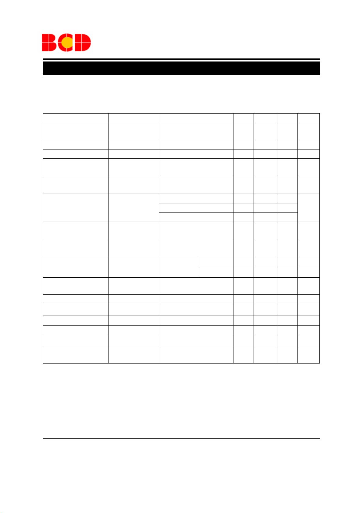
AP2125-1.8 Electrical Characteristics
(VIN=2.8V, TA=25oC, CIN=1μF, C
Parameter Symbol Conditions Min Typ Max Unit
Output Voltage
Input Voltage V
Maximum Output Current I
Load Regulation
Line Regulation
Dropout Voltage
OUT
OUT(MAX)
V
V
=1μF,
V
OUT
IN
RLOAD
RLINE
V
DROP
Bold
typeface applies over -40oC≤TJ≤
VIN=2.8V
1mA≤I
VIN-V
OUT
OUT
≤30mA
=1V, V
VIN=2.8V
OUT
≤300mA
1mA≤I
2.8V≤VIN≤6V
=30mA
I
OUT
I
=10mA 10 12
OUT
=100mA 100 120
I
OUT
=300mA 300 360
I
OUT
85oC,
unless otherwise specified.)
1.764 1.8 1.836 V
6V
=1.76V 300 360 mA
OUT
615mV
115mV
mV
Quiescent Current
Standby Current
Power Supply
Rejection Ratio
Output Voltage
Temperature Coefficient
(ΔV
OUT/VOUT
Short Current Limit I
RMS Output Noise
I
I
STD
PSRR
SHORT
V
NOISE
Q
VIN=2.8V, I
VIN=2.8V
V
Ripple 0.5Vp-p
V
)/ΔTI
OUT
V
10Hz ≤f≤100kHz
in OFF mode
CE
OUT
=0mA
60 90
0.01 1.0
f=100Hz 70 dB
=2.8V
IN
=30mA
=0V 50 mA
OUT
f=1KHz 70 dB
±100
50
μA
μA
ppm/
μVrm s
CE "High" Voltage CE input voltage "High" 1.5 V
CE "Low" Voltage CE input voltage "Low" 0.4 V
Thermal Shutdown 160
Thermal Shutdown Hysteresis
25
o
o
o
C
C
C
BCD Semiconductor Manufacturing LimitedSep. 2012 Rev. 1. 5
6
Page 7
Data Sheet
300mA HIGH SPEED, EXTREMELY LOW NOISE CMOS LDO REGULATOR AP2125
Electrical Characteristics (Continued)
AP2125-2.5 Electrical Characteristics
(VIN=3.5V, TA=25oC, CIN=1μF, C
Parameter Symbol Conditions Min Typ Max Unit
Output Voltage
Input Voltage V
Maximum Output Current I
Load Regulation
Line Regulation
Dropout Voltage
OUT
OUT(MAX)
V
V
=1μF,
V
OUT
IN
RLOAD
RLINE
V
DROP
Bold
typeface applies over -40oC≤TJ≤
VIN=3.5V
1mA≤I
VIN-V
OUT
OUT
≤30mA
=1V, V
VIN=3.5V
OUT
≤300mA
1mA≤I
3.5V≤VIN≤6V
=30mA
I
OUT
I
=10mA 6.5 10
OUT
=100mA 65 100
I
OUT
=300mA 200 300
I
OUT
85oC,
unless otherwise specified.)
2.45 2.5 2.55 V
6V
=2.45V 300 360 mA
OUT
10 15 mV
115mV
mV
Quiescent Current
Standby Current
Power Supply
Rejection Ratio
Output Voltage
Temperature Coefficient
(ΔV
OUT/VOUT
Short Current Limit I
RMS Output Noise
I
I
STD
PSRR
SHORT
V
NOISE
Q
VIN=3.5V, I
VIN=3.5V
V
Ripple 0.5Vp-p
V
)/ΔTI
OUT
V
10Hz ≤f≤100kHz
in OFF mode
CE
OUT
=0mA
60 90
0.01 1.0
f=100Hz 65 dB
=3.5V
IN
=30mA
=0V 50 mA
OUT
f=1KHz 65 dB
±100
50
μA
μA
ppm/
μVrm s
CE "High" Voltage CE input voltage "High" 1.5 V
CE "Low" Voltage CE input voltage "Low" 0.4 V
Thermal Shutdown 160
Thermal Shutdown Hysteresis
25
o
o
o
C
C
C
Sep. 2012 Rev. 1. 5 BCD Semiconductor Manufacturing Limited
7
Page 8

Data Sheet
300mA HIGH SPEED, EXTREMELY LOW NOISE CMOS LDO REGULATOR AP2125
Electrical Characteristics (Continued)
AP2125-2.8 Electrical Characteristics
(VIN=3.8V, TA=25oC, CIN=1μF, C
Parameter Symbol Conditions Min Typ Max Unit
Output Voltage
Input Voltage V
Maximum Output Current I
Load Regulation
Line Regulation
Dropout Voltage
OUT
OUT(MAX)
V
V
=1μF,
V
OUT
IN
RLOAD
RLINE
V
DROP
Bold
typeface applies over -40oC≤TJ≤
VIN=3.8V
1mA≤I
VIN-V
OUT
OUT
≤30mA
=1V, V
VIN=3.8V
OUT
≤300mA
1mA≤I
3.8V≤VIN≤6V
=30mA
I
OUT
I
=10mA 6.5 10
OUT
=100mA 65 100
I
OUT
=300mA 200 300
I
OUT
85oC,
unless otherwise specified.)
2.744 2.8 2.856 V
6V
=2.74V 300 360 mA
OUT
11 15 m V
115mV
mV
Quiescent Current
Standby Current
Power Supply
Rejection Ratio
Output Voltage
Temperature Coefficient
(ΔV
OUT/VOUT
Short Current Limit I
RMS Output Noise
I
I
STD
PSRR
SHORT
V
NOISE
Q
VIN=3.8V, I
VIN=3.8V
V
Ripple 0.5Vp-p
V
)/ΔTI
OUT
V
10Hz ≤f≤100kHz
in OFF mode
CE
OUT
=0mA
60 90
0.01 1.0
f=100Hz 65 dB
=3.8V
IN
=30mA
=0V 50 mA
OUT
f=1KHz 65 dB
±100
50
μA
μA
ppm/
μVrm s
CE "High" Voltage CE input voltage "High" 1.5 V
CE "Low" Voltage CE input voltage "Low" 0.4 V
Thermal Shutdown 160
Thermal Shutdown Hysteresis
25
o
o
o
C
C
C
BCD Semiconductor Manufacturing LimitedSep. 2012 Rev. 1. 5
8
Page 9

Data Sheet
300mA HIGH SPEED, EXTREMELY LOW NOISE CMOS LDO REGULATOR AP2125
Electrical Characteristics (Continued)
AP2125-3.0 Electrical Characteristics
(VIN=4.0V, TA=25oC, CIN=1μF, C
Parameter Symbol Conditions Min Typ Max Unit
Output Voltage
Input Voltage V
Maximum Output Current I
Load Regulation
Line Regulation
Dropout Voltage
OUT
OUT(MAX)
V
V
=1μF,
V
OUT
IN
RLOAD
RLINE
V
DROP
Bold
typeface applies over -40oC≤TJ≤
VIN=4.0V
1mA≤I
VIN-V
OUT
OUT
≤30mA
=1V, V
VIN=4.0V
OUT
≤300mA
1mA≤I
4.0V≤VIN≤6V
=30mA
I
OUT
I
=10mA 6.5 10
OUT
=100mA 65 100
I
OUT
=300mA 200 300
I
OUT
85oC,
unless otherwise specified.)
2.94 3.0 3.06 V
6V
=2.94V 300 360 mA
OUT
12 15 mV
115mV
mV
Quiescent Current
Standby Current
Power Supply
Rejection Ratio
Output Voltage
Temperature Coefficient
(ΔV
OUT/VOUT
Short Current Limit I
RMS Output Noise
I
I
STD
PSRR
SHORT
V
NOISE
Q
VIN=4.0V, I
VIN=4.0V
V
Ripple 0.5Vp-p
V
)/ΔTI
OUT
V
10Hz ≤f≤100kHz
in OFF mode
CE
OUT
=0mA
60 90
0.01 1.0
f=100Hz 65 dB
=4.0V
IN
=30mA
=0V 50 mA
OUT
f=1KHz 65 dB
±100
50
μA
μA
ppm/
μVrm s
CE "High" Voltage CE input voltage "High" 1.5 V
CE "Low" Voltage CE input voltage "Low" 0.4 V
Thermal Shutdown 160
Thermal Shutdown Hysteresis
25
o
o
o
C
C
C
Sep. 2012 Rev. 1. 5 BCD Semiconductor Manufacturing Limited
9
Page 10

Data Sheet
300mA HIGH SPEED, EXTREMELY LOW NOISE CMOS LDO REGULATOR AP2125
Electrical Characteristics (Continued)
AP2125-3.3 Electrical Characteristics
(VIN=4.3V, TA=25oC, CIN=1μF, C
Parameter Symbol Conditions Min Typ Max Unit
Output Voltage
Input Voltage V
Maximum Output Current I
Load Regulation
Line Regulation
Dropout Voltage
OUT
OUT(MAX)
V
V
=1μF,
V
OUT
IN
RLOAD
RLINE
V
DROP
Bold
typeface applies over -40oC≤TJ≤
VIN=4.3V
1mA≤I
VIN-V
OUT
OUT
≤30mA
=1V, V
VIN=4.3V
OUT
≤300mA
1mA≤I
4.3V≤VIN≤6V
=30mA
I
OUT
I
=10mA 6.5 10
OUT
=100mA 65 100
I
OUT
=300mA 200 300
I
OUT
85oC,
unless otherwise specified.)
3.234 3.3 3.366 V
6V
=3.23V 300 360 mA
OUT
13 15 mV
115mV
mV
Quiescent Current
Standby Current
Power Supply
Rejection Ratio
Output Voltage
Temperature Coefficient
(ΔV
OUT/VOUT
Short Current Limit I
RMS Output Noise
I
I
STD
PSRR
SHORT
V
NOISE
Q
VIN=4.3V, I
VIN=4.3V
V
Ripple 0.5Vp-p
V
)/ΔTI
OUT
V
10Hz ≤f≤100kHz
in OFF mode
CE
OUT
=0mA
60 90
0.01 1.0
f=100Hz 65 dB
=4.3V
IN
=30mA
=0V 50 mA
OUT
f=1KHz 65 dB
±100
50
μA
μA
ppm/
μVrm s
CE "High" Voltage CE input voltage "High" 1.5 V
CE "Low" Voltage CE input voltage "Low" 0.4 V
Thermal Shutdown 160
Thermal Shutdown Hysteresis
25
o
o
o
C
C
C
10
BCD Semiconductor Manufacturing LimitedSep. 2012 Rev. 1. 5
Page 11

Data Sheet
300mA HIGH SPEED, EXTREMELY LOW NOISE CMOS LDO REGULATOR AP2125
Electrical Characteristics (Continued)
AP2125-4.15 Electrical Characteristics
(VIN=5.15V, TA=25oC, CIN=1μF, C
Parameter Symbol Conditions Min Typ Max Unit
Output Voltage
Input Voltage V
Maximum Output Current I
Load Regulation
Line Regulation
V
V
Dropout Voltage
=1μF,
OUT
V
OUT
IN
OUT(MAX)
RLOAD
RLINE
V
DROP
Bold
typeface applies over -40oC≤TJ≤
VIN=5.15V
1mA≤I
VIN-V
OUT
OUT
≤30mA
=1V, V
OUT
VIN=5.15V
OUT
≤300mA
1mA≤I
5.15V≤VIN≤6V
=30mA
I
OUT
I
=10mA 6.5 10
OUT
=100mA 65 100
I
OUT
=300mA 200 300
I
OUT
85oC,
unless otherwise specified.)
4.067 4.15 4.233 V
6V
=4.06V 300 360 mA
13 15 mV
115mV
mV
Quiescent Current
Standby Current
Power Supply
Rejection Ratio
Output Voltage
Temperature Coefficient
(ΔV
OUT/VOUT
Short Current Limit I
RMS Output Noise
I
I
STD
PSRR
SHORT
V
NOISE
Q
VIN=5.15V, I
VIN=5.15V
V
Ripple 0.5Vp-p
V
)/ΔTI
OUT
V
10Hz ≤f≤100kHz
in OFF mode
CE
OUT
=0mA
60 90
0.01 1.0
f=100Hz 65 dB
=5.15V
IN
=30mA
=0V 50 mA
OUT
f=1KHz 65 dB
±100
50
μA
μA
ppm/
μVrm s
CE "High" Voltage CE input voltage "High" 1.5 V
CE "Low" Voltage CE input voltage "Low" 0.4 V
Thermal Shutdown 160
Thermal Shutdown Hysteresis
25
o
o
o
C
C
C
Sep. 2012 Rev. 1. 5 BCD Semiconductor Manufacturing Limited
11
Page 12

Data Sheet
300mA HIGH SPEED, EXTREMELY LOW NOISE CMOS LDO REGULATOR AP2125
Electrical Characteristics (Continued)
AP2125-4.2 Electrical Characteristics
(VIN=5.2V, TA=25oC, CIN=1μF, C
Parameter Symbol Conditions Min Typ Max Unit
Output Voltage
Input Voltage V
Maximum Output Current I
Load Regulation
Line Regulation
Dropout Voltage
OUT
OUT(MAX)
V
V
=1μF,
V
OUT
IN
RLOAD
RLINE
V
DROP
Bold
typeface applies over -40oC≤TJ≤
VIN=5.2V
1mA≤I
VIN-V
OUT
OUT
≤30mA
=1V, V
VIN=5.2V
OUT
≤300mA
1mA≤I
5.2V≤VIN≤6V
=30mA
I
OUT
I
=10mA 6.5 10
OUT
=100mA 65 100
I
OUT
=300mA 200 300
I
OUT
85oC,
unless otherwise specified.)
4.116 4.2 4.284 V
6V
=4.12V 300 360 mA
OUT
13 15 mV
115mV
mV
Quiescent Current
Standby Current
Power Supply
Rejection Ratio
Output Voltage
Temperature Coefficient
(ΔV
OUT/VOUT
Short Current Limit I
RMS Output Noise
I
I
STD
PSRR
SHORT
V
NOISE
Q
VIN=5.2V, I
VIN=5.2V
V
Ripple 0.5Vp-p
V
)/ΔTI
OUT
V
10Hz ≤f≤100kHz
in OFF mode
CE
OUT
=0mA
60 90
0.01 1.0
f=100Hz 65 dB
=5.2V
IN
=30mA
=0V 50 mA
OUT
f=1KHz 65 dB
±100
50
μA
μA
ppm/
μVrm s
CE "High" Voltage CE input voltage "High" 1.5 V
CE "Low" Voltage CE input voltage "Low" 0.4 V
Thermal Shutdown 160
Thermal Shutdown Hysteresis
25
o
o
o
C
C
C
12
BCD Semiconductor Manufacturing LimitedSep. 2012 Rev. 1. 5
Page 13

Data Sheet
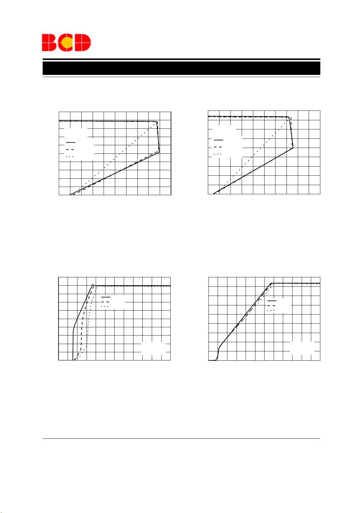
0 50 100 150 200 250 300
1.70
1.72
1.74
1.76
1.78
1.80
1.82
1.84
1.86
1.88
1.90
AP2125-1.8
VIN=2.8V
TC=25oC
Output Voltage (V)
Output Current (mA)
0 50 100 150 200 250 300
3.30
3.32
3.34
3.36
3.38
3.40
3.42
3.44
3.46
3.48
3.50
AP2125-3.3
VIN=4.3V
TC=25oC
Output Voltage (V)
Output Current (mA)
0 30 60 90 120 150 180 210 240 270 300
0
40
80
120
160
200
240
280
320
360
400
AP2125-1.8
VIN=2.8V
TC=-40oC
TC=25oC
TC=85oC
Dropout Voltage (mV)
Output Current (mA)
0 30 60 90 120 1 50 180 210 240 270 300
0
40
80
120
160
200
240
280
320
360
400
TC=-40oC
T
C
=25oC
TC=85oC
AP2125-3.3
V
IN
=4.3V
Dropout Voltage (mV)
Output Current (mA)
300mA HIGH SPEED, EXTREMELY LOW NOISE CMOS LDO REGULATOR AP2125
Typical Performance Characteristics
Figure 4. Output Voltage vs. Output Current
Figure 6. Dropout Voltage vs. Output Current
Figure 5. Output Voltage vs. Output Current
Figure 7. Dropout Voltage vs. Output Current
Sep. 2012 Rev. 1. 5 BCD Semiconductor Manufacturing Limited
13
Page 14

Data Sheet
-25 0 25 50 75
0
40
80
120
160
200
240
280
320
360
400
AP2125-1.8
V
IN
=2.8V
I
OUT
=10mA
I
OUT
=100mA
I
OUT
=200mA
I
OUT
=300mA
Dropout Voltage (mV)
Case Temperature (oC)
0 50 100 150 200 250 300 350 400 450 500
0.0
0.2
0.4
0.6
0.8
1.0
1.2
1.4
1.6
1.8
2.0
AP2125-1.8
T
C
=25oC
Output Voltage (V)
Output Current (mA)
VIN=2.8V
VIN=6V
-25 0 25 50 75
0
40
80
120
160
200
240
280
320
360
400
AP2125-3.3
V
IN
=4.3V
I
OUT
=10mA
I
OUT
=100mA
I
OUT
=200mA
I
OUT
=300mA
Dropout Voltage (mV)
Case Temperature (oC)
0 50 100 150 200 250 300 350 400 450 500
0.0
0.4
0.8
1.2
1.6
2.0
2.4
2.8
3.2
3.6
AP2125-3.3
T
C
=25oC
Output Voltage (V)
Output Current (mA)
VIN=4.3V
VIN=6V
300mA HIGH SPEED, EXTREMELY LOW NOISE CMOS LDO REGULATOR AP2125
Typical Performance Characteristics (Continued)
Figure 8. Dropout Voltage vs. Case Temperature
Figure 10. Current Limit
Figure 9. Dropout Voltage vs. Case Temperature
Figure 11. Current Limit
BCD Semiconductor Manufacturing LimitedSep. 2012 Rev. 1. 5
14
Page 15
Data Sheet
0 50 100 150 200 250 300 350 400 450 500
0.0
0.2
0.4
0.6
0.8
1.0
1.2
1.4
1.6
1.8
2.0
AP2125-1.8
V
IN
=2.8V
Output Voltage (V)
Output Current (mA)
TC=-40oC
TC=25oC
TC=85oC
0 50 100 150 200 250 300 350 400 450 500
0.0
0.4
0.8
1.2
1.6
2.0
2.4
2.8
3.2
3.6
AP2125-3.3
V
IN
=4.3V
Output Voltage (V)
Output Current (mA)
TC=-40oC
TC=25oC
TC=85oC
0.0 0.5 1.0 1.5 2.0 2.5 3.0 3.5 4.0 4.5 5.0 5.5 6.0
0.0
0.2
0.4
0.6
0.8
1.0
1.2
1.4
1.6
1.8
2.0
AP2125-1.8
T
C
=25oC
Output Voltage (V)
Input Voltage (V)
1mA
100mA
300mA
0.0 0.5 1.0 1.5 2.0 2.5 3.0 3.5 4.0 4.5 5.0 5.5 6.0
0.0
0.4
0.8
1.2
1.6
2.0
2.4
2.8
3.2
3.6
AP2125-3.3
T
C
=25oC
Output Voltage (V)
Input Voltage (V)
1mA
100mA
300mA
300mA HIGH SPEED, EXTREMELY LOW NOISE CMOS LDO REGULATOR AP2125
Typical Performance Characteristics (Continued)
Figure 12. Current Limit
Figure 13. Current Limit
Figure 14. Output Voltage vs. Input Voltage Figure 15. Output Voltage vs. Input Voltage
Sep. 2012 Rev. 1. 5 BCD Semiconductor Manufacturing Limited
15
Page 16

Data Sheet
-25 0 25 50 75
1.70
1.72
1.74
1.76
1.78
1.80
1.82
1.84
1.86
1.88
1.90
AP2125-1.8
V
IN
=2.8V
Output Voltage (V)
Case Temperature (oC)
I
OUT
=10mA
I
OUT
=30mA
I
OUT
=100mA
I
OUT
=300mA
0.00.51.01.52.02.53.03.54.04.55.05.56.0
0.0
0.2
0.4
0.6
0.8
1.0
1.2
1.4
1.6
1.8
2.0
AP2125-1.8
T
C
=25oC
No Load
Output Voltage (V)
Input Voltage (V)
TC=-40oC
TC=25oC
TC=85oC
0.00.51.01.52.02.53.03.54.04.55.05.56.0
0.0
0.4
0.8
1.2
1.6
2.0
2.4
2.8
3.2
3.6
AP2125-3.3
T
C
=25oC
No Load
Output Voltage (V)
Input Voltage (V)
TC=-40oC
TC=25oC
TC=85oC
-25 0 25 50 75
3.20
3.22
3.24
3.26
3.28
3.30
3.32
3.34
3.36
3.38
3.40
AP2125-3.3
V
IN
=4.3V
Output Voltage (V)
Case Temperature (oC)
I
OUT
=10mA
I
OUT
=30mA
I
OUT
=100mA
I
OUT
=300mA
300mA HIGH SPEED, EXTREMELY LOW NOISE CMOS LDO REGULATOR AP2125
Typical Performance Characteristics (Continued)
Figure 16. Output Voltage vs. Input Voltage
Figure 18. Output Voltage vs. Case Temperature
Figure 17. Output Voltage vs. Input Voltage
Figure 19. Output Voltage vs. Case Temperature
BCD Semiconductor Manufacturing LimitedSep. 2012 Rev. 1. 5
16
Page 17

Data Sheet
0123456
0
10
20
30
40
50
60
70
80
90
100
AP2125-1.8
No Load
TC=-40oC
TC=25oC
TC=85oC
Supply Current (μA)
Input Voltage (V)
0123456
0
10
20
30
40
50
60
70
80
90
100
TC=-40oC
TC=25oC
TC=85oC
AP2125-3.3
No Load
Supply Current (μA)
Input Voltage (V)
-40 -20 0 20 40 60 80
40
44
48
52
56
60
64
68
72
76
80
Supply Current (μA)
Case Temperature (oC)
AP2125-1.8
V
IN
=2.8V
No Load
-40-20 0 20406080
40
44
48
52
56
60
64
68
72
76
80
AP2125-3.3
V
IN
=4.3V
No Load
Supply Current (μA)
Case Temperature (oC)
300mA HIGH SPEED, EXTREMELY LOW NOISE CMOS LDO REGULATOR AP2125
Typical Performance Characteristics (Continued)
Figure 20. Supply Current vs. Input Voltage
Figure 22. Supply Current vs. Case Temperature
Sep. 2012 Rev. 1. 5 BCD Semiconductor Manufacturing Limited
Figure 21. Supply Current vs. Input Voltage
Figure 23. Supply Current vs. Case Temperature
17
Page 18

Data Sheet
0 50 100 150 200 250 300 350 400 450 500
0
10
20
30
40
50
60
70
80
90
100
110
120
130
AP2125-1.8
V
IN
=2.8V
Supply Current (μA)
Output Current (mA)
TC=-40oC
TC=25oC
TC=85oC
0 50 100 150 200 250 300 350 400
0
10
20
30
40
50
60
70
80
90
100
110
120
130
140
150
AP2125-3.3
V
IN
=4.3V
Supply Current (μA)
Output Current (mA)
TC=-40oC
TC=25oC
TC=85oC
0 40 80 120 160 200 240 280 320 360 400 440 480
0
10
20
30
40
50
60
70
80
90
100
110
120
AP2125-1.8
TC=25oC
Supply Current (μA)
Output Current (mA)
VIN=2.8V
VIN=6V
0 40 80 120 160 200 240 280 320 360 400
0
15
30
45
60
75
90
105
120
135
150
AP2125-3.3
T
C
=25oC
Supply Current (μA)
Output Current (mA)
VIN=4.3V
VIN=6V
300mA HIGH SPEED, EXTREMELY LOW NOISE CMOS LDO REGULATOR AP2125
Typical Performance Characteristics (Continued)
Figure 24. Supply Current vs. Output Current
Figure 26. Supply Current vs. Output Current
Figure 25. Supply Current vs. Output Current
Figure 27. Supply Current vs. Output Current
BCD Semiconductor Manufacturing LimitedSep. 2012 Rev. 1. 5
18
Page 19

Data Sheet
300mA HIGH SPEED, EXTREMELY LOW NOISE CMOS LDO REGULATOR AP2125
Typical Performance Characteristics (Continued)
4.8
3.8
( 1 V / D i v )
IN
V
2.8
0.02
0
-0.02
(0 .02 V/D iv)
OUT
V
Δ
(Conditions: I
1.84
1.82
(0.02V/Div)
OUT
1.8
V
Time (40μs/Div)
Figure 28. Line Transient
=30mA, C
OUT
=1μF, VIN=2.8 to 3.8V)
OUT
AP2125-1.8
AP2125-1.8
5
4.5
(0.5V/Div)
IN
4
V
0.05
0
(0 .05 V/D iv)
-0.05
OUT
V
Δ
(Conditions: I
3.34
3.32
(0.02V/Div)
OUT
3.3
V
Time (100μs/Div)
Figure 29. Line Transient
=30mA, C
OUT
=1μF, VIN=4 to 5V)
OUT
AP2125-3.3
AP2125-3.3
100
50
(50mA/Div)
OUT
0
I
Time (40μs/Div)
Figure 30. Load Transient
(Conditions: I
C
=10 to 100mA, CIN=1μF,
OUT
=1μF, VIN=2.8 V)
OUT
100
50
(50mA/Div)
OUT
0
I
Time (40μs/Div)
Figure 31. Load Transient
(Conditions: I
C
=10 to 100mA, CIN=1μF,
OUT
=1μF, VIN=4.3 V)
OUT
Sep. 2012 Rev. 1. 5 BCD Semiconductor Manufacturing Limited
19
Page 20

Data Sheet
10 100 1k 10k 100k
0
10
20
30
40
50
60
70
80
90
100
PSRR (dB)
Frequency (Hz)
AP2125-1.8
VIN=2.8V
I
OUT
=30mA
10 100 1k 10k 100k
0
10
20
30
40
50
60
70
80
90
100
PSRR (dB)
Frequency (Hz)
AP2125-3.3
VIN=4.3V
I
OUT
=30mA
0 50 100 150 200 250 300
0.1
1
10
100
1000
Stable Area
AP2125-1.8
C
IN
= 1μF
C
OUT
= 1μF
ESR (Ω)
Output Current (mA)
300mA HIGH SPEED, EXTREMELY LOW NOISE CMOS LDO REGULATOR AP2125
Typical Performance Characteristics (Continued)
3
2
(1V/Div)
CE
V
1
AP2125-2.8
0
3
2
(1V/Div)
OUT
1
v
0
Time (200μs/Div)
Figure 32. Enable Input Response and Auto-discharge
(Conditions: V
C
=1μF, VIN=3V, no load)
OUT
=0 to 3V, CIN=1μF,
CE
Figure 33. ESR vs. Output Current
Figure 34. PSRR
Figure 35. PSRR
BCD Semiconductor Manufacturing LimitedSep. 2012 Rev. 1. 5
20
Page 21

Data Sheet
30 40 50 60 70 80 90 100 110 120
0
50
100
150
200
250
300
350
400
450
500
550
600
Power Dissipation (mW)
Ambient Temperature (oC)
AP2125-1.8
Package: SC-70-5
No Heatsink
30 40 50 60 70 80 90 100 110 120
0
100
200
300
400
500
600
700
800
Power Dissipation (mW)
Ambient Temperature (oC)
AP2125-3.3
Package: SC-70-5
No Heatsink
300mA HIGH SPEED, EXTREMELY LOW NOISE CMOS LDO REGULATOR AP2125
Typical Performance Characteristics (Continued)
Figure 36. Power Dissipation vs. Ambient Temperature
Sep. 2012 Rev. 1. 5 BCD Semiconductor Manufacturing Limited
Figure 37. Power Dissipation vs. Ambient Temperature
21
Page 22

Data Sheet
V
IN
AP2125-1.8
C
IN
1μF
C
OUT
1μF
V
OUT
V
IN
V
OUT
GND
V
IN
AP2125-3.0
C
IN
1μF
C
OUT
1μF
V
OUT
V
IN
V
OUT
GND
CE
NC
VIN=2.8V
V
OUT
=1.8V
V
OUT
=3VVIN=4V
300mA HIGH SPEED, EXTREMELY LOW NOISE CMOS LDO REGULATOR AP2125
Typical Application
Figure 38. Typical Application of AP2125
22
BCD Semiconductor Manufacturing LimitedSep. 2012 Rev. 1. 5
Page 23
Data Sheet
2.820(0.111)
3.020(0.119)
2.650(0.104)
2.950(0.116)
0.950(0.037)
TYP
0.300(0.012)
0.500(0.020)
1.500(0.059)
1.700(0.067)
1.800(0.071)
2.000(0.079)
0.300(0.012)
0.600(0.024)
0.100(0.004)
0.200(0.008)
0.000(0.000)
0.150(0.006)
0.900(0.035)
1.300(0.051)
1.450(0.057)
MAX.
0.200(0.008)
0
8
300mA HIGH SPEED, EXTREMELY LOW NOISE CMOS LDO REGULATOR AP2125
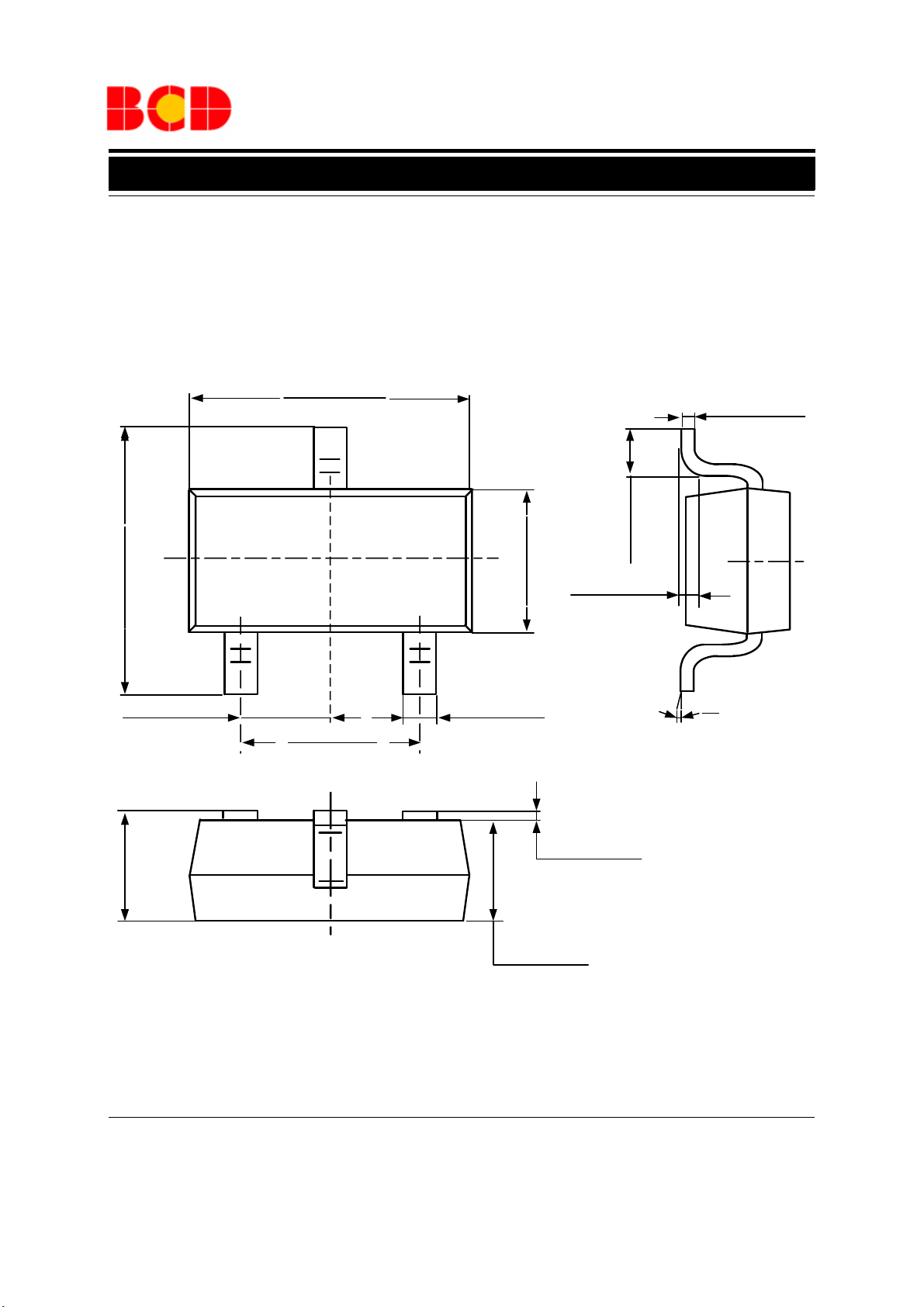
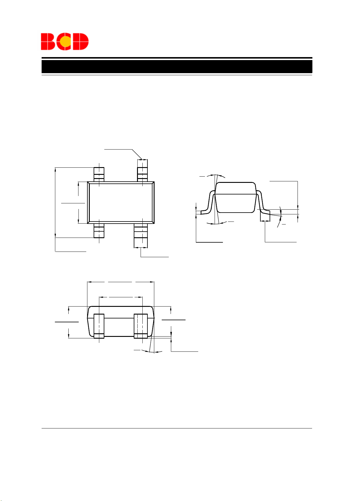
Mechanical Dimensions
SOT-23-3 Unit: mm(inch)
°
°
Sep. 2012 Rev. 1. 5 BCD Semiconductor Manufacturing Limited
23
Page 24

Data Sheet
2.820(0.111)
2
.
6
5
0
(
0
.
1
0
4
)
1
.
5
0
0
(
0
.
0
5
9
)
0
.
0
0
0
(
0
.
0
0
0
)
0.300(0.012)
0.950(0.037)
0
.
9
0
0
(
0
.
0
3
5
)
0.100(0.004)
0.200(0.008)
0
.
3
0
0
(
0
.
0
1
2
)
8°
0°
3.020(0.119)
1
.
7
0
0
(
0
.
0
6
7
)
2
.
9
5
0
(
0
.
1
1
6
)
0.400(0.016)
0
.
1
5
0
(
0
.
0
0
6
)
1
.
3
0
0
(
0
.
0
5
1
)
0.200(0.008)
0
.
6
0
0
(
0
.
0
2
4
)
1.800(0.071)
2.000(0.079)
0
.
7
0
0
(
0
.
0
2
8
)
R
E
F
T
Y
P
1
.
4
5
0
(
0
.
0
5
7
)
M
A
X
300mA HIGH SPEED, EXTREMELY LOW NOISE CMOS LDO REGULATOR AP2125
Mechanical Dimensions (Continued)
SOT-23-5 Unit: mm(inch)
24
BCD Semiconductor Manufacturing LimitedSep. 2012 Rev. 1. 5
Page 25

Data Sheet
2.000(0.079)
2.200(0.087)
2.150(0.085)
2.450(0.096)
1.150(0.045)
1.350(0.053)
0.650(0.026)TYP
1.200(0.047)
1.400(0.055)
0.150(0.006)
0.350(0.014)
0.525(0.021)REF
0.080(0.003)
0.150(0.006)
0°
8°
0.200(0.008)
0.260(0.010)
0.460(0.018)
0.000(0.000)
0.100(0.004)
0.900(0.035)
1.000(0.039)
0.900(0.035)
1.100(0.043)
300mA HIGH SPEED, EXTREMELY LOW NOISE CMOS LDO REGULATOR AP2125
Mechanical Dimensions (Continued)
SC-70-5 Unit: mm(inch)
Sep. 2012 Rev. 1. 5 BCD Semiconductor Manufacturing Limited
25
Page 26
Data Sheet
1.800(0.071)
2.400(0.094)
1.150(0.045)
1.350(0.053)
0.250(0.010)
0.400(0.016)
0.350(0.014)
0.500(0.020)
1.300(0.051)
Typ
1.800(0.071)
2.200(0.087)
0.700(0.027)
1.000(0.039)
0.800(0.031)
1.100(0.043)
0.000(0.000)
0.100(0.004)
0.100(0.004)
0.260(0.010)
0.260(0.010)
0.460(0.018)
0.150(0.006)
Typ
4
12
4
12
4
12
0
8
300mA HIGH SPEED, EXTREMELY LOW NOISE CMOS LDO REGULATOR AP2125
Mechanical Dimensions (Continued)
SC-82 Unit: mm(inch)
°
°
°
°
°
°
°
°
BCD Semiconductor Manufacturing LimitedSep. 2012 Rev. 1. 5
26
Page 27
BCD Semiconductor Manufacturing Limited
IMPORTANT NOTICE
IMPORTANT NOTICE
BCD Semiconductor Manufacturing Limited reserves the right to make changes without further notice to any products or specifi-
BCD Semiconductor Manufacturing Limited reserves the right to make changes without further notice to any products or specifi-
cations herein. BCD Semiconductor Manufacturing Limited does not assume any responsibility for use of any its products for any
cations herein. BCD Semiconductor Manufacturing Limited does not assume any responsibility for use of any its products for any
particular purpose, nor does BCD Semiconductor Manufacturing Limited assume any liability arising out of the application or use
particular purpose, nor does BCD Semiconductor Manufacturing Limited assume any liability arising out of the application or use
of any its products or circuits. BCD Semiconductor Manufacturing Limited does not convey any license under its patent rights or
of any its products or circuits. BCD Semiconductor Manufacturing Limited does not convey any license under its patent rights or
other rights nor the rights of others.
other rights nor the rights of others.
http://www.bcdsemi.com
MAIN SITE
MAIN SITE
- Headquarters
BCD Semiconductor Manufacturing Limited
BCD Semiconductor Manufactur ing Limited
- Wafer Fab
No. 1600, Zi Xing Road, Shanghai ZiZhu Science-based Industrial Park, 200241, China
Shanghai SIM-BCD Semiconductor Manufacturing Limited
Tel: +86-21-24162266, Fax: +86-21-24162277
800, Yi Shan Road, Shanghai 200233, China
Tel: +86-21-6485 1491, Fax: +86-21-5450 0008
REGIONAL SALES OFFICE
Shenzhen Office
REGIONAL SALES OFFICE
Shanghai SIM-BCD Semiconductor Manufacturing Co., Ltd., Shenzhen Office
Shenzhen Office
Unit A Room 1203, Skyworth Bldg., Gaoxin Ave.1.S., Nanshan District, Shenzhen,
Shanghai SIM-BCD Semiconductor Manufacturing Co., Ltd. Shenzhen Office
China
Advanced Analog Circuits (Shanghai) Corporation Shenzhen Office
Tel: +86-755-8826 7951
Room E, 5F, Noble Center, No.1006, 3rd Fuzhong Road, Futian District, Shenzhen 518026, China
Fax: +86-755-8826 7865
Tel: +86-755-8826 7951
Fax: +86-755-8826 7865
- Wafer Fab
BCD Semiconductor Manufacturing Limited
Shanghai SIM-BCD Semiconductor Manufacturing Co., Ltd.
- IC Design Group
800 Yi Shan Road, Shanghai 200233, China
Advanced Analog Circuits (Shanghai) Corporation
Tel: +86-21-6485 1491, Fax: +86-21-5450 0008
8F, Zone B, 900, Yi Shan Road, Shanghai 200233, China
Tel: +86-21-6495 9539, Fax: +86-21-6485 9673
Taiwan Office
BCD Semiconductor (Taiwan) Company Limited
Taiwan Office
4F, 298-1, Rui Guang Road, Nei-Hu District, Taipei,
BCD Semiconductor (Taiwan) Company Limited
Tai wan
4F, 298-1, Rui Guang Road, Nei-Hu District, Taipei,
Tel: +886-2-2656 2808
Taiwan
Fax: +886-2-2656 2806
Tel: +886-2-2656 2808
Fax: +886-2-2656 2806
USA Office
BCD Semiconductor Corp.
USA Office
30920 Huntwood Ave. Hayward,
BCD Semiconductor Corporation
CA 94544, USA
30920 Huntwood Ave. Hayward,
Tel : +1-510-324-2988
CA 94544, U.S.A
Fax: +1-510-324-2788
Tel : +1-510-324-2988
Fax: +1-510-324-2788
 Loading...