

Page 1
Data Sheet
HIGH SPEED, EXTREMELY LOW NOISE LDO REGULATOR AP2120
General Description
The AP2120 series are positive voltage regulator ICs
fabricated by CMOS process. Each of these ICs consists of a voltage reference, an error amplifier, a resistor network for setting output voltage, a current limit
circuit for current protection.
The AP2120 series feature high supply voltage ripple
rejection, low dropout voltage, low noise, high output
voltage accuracy, and low current consumption which
make them ideal for use in various battery-powered
devices.
The AP2120 series have 1.2V, 1.3V, 1.5V, 1.8V, 2.5V,
2.8V, 3.0V, 3.2V, 3.3V, 3.6V, 4.0V and 5.0V versions.
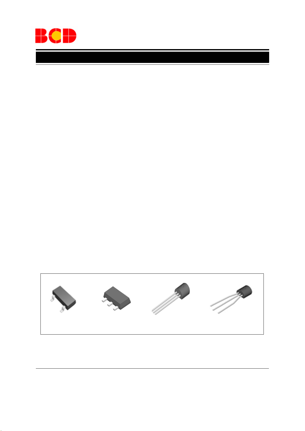
The AP2120 are available in standard SOT-23, SOT-89
and TO-92 packages.
Features
· Low Dropout Voltage at I
Typical (Except 1.2V, 1.3V and 1.5V Versions)
· Low Quiescent Current: 25μA Typical
· High Ripple Rejection: 65dB Typical (f=1kHz)
· Output Current: More Than 150mA (250mA
Limit)
· Extremely Low Noise: 15μVrm s@ V
1.3V, 1.5V (10Hz to 100kHz)
· Excellent Line Regulation: 4mV Typical
· Excellent Load Regulation: 12mV Typical
· High Output Voltage Accuracy: ±2%
· Excellent Line Transient Response and Load
Transient Response
· Compatible with Low ESR Ceramic Capacitor (as
Low as 1μF)
=100mA: 200mV
OUT
OUT
=1.2V,
Applications
· Mobile Phones, Cordless Phones
· Wireless Communication Equipment
· Portable Games
· Cameras, Video Recorders
· Sub-board Power Supplies for Telecom Equip-
ment
· Battery Powered Equipment
SOT-23
Mar. 2013 Rev. 1. 4 BCD Semiconductor Manufacturing Limited
SOT-89
Figure 1. Package Types of AP2120
TO-92 (Bulk Packing)
1
TO-92 (Ammo Packing)
Page 2
Data Sheet
3
2
1
3
2
1
1
2
3
1
2
3
123
HIGH SPEED, EXTREMELY LOW NOISE LDO REGULATOR AP2120
Pin Configuration
GND
N
V
V
N/NA Package
(SOT-23)
IN
OUT
Z Package
(TO-92 (Bulk Packing))
V
V
NA
GND
V
OUT
IN
IN
V
R Package
(SOT-89)
OUT
GND
Z Package
(TO-92 (Ammo Packing))
V
V
OUT
IN
V
V
IN
OUT
GND
Figure 2. Pin Configuration of AP2120 (Top View)
GND
Pin Description
Pin Number
SOT-23 (N) SOT-23 (NA) SOT-89/
TO-92
1 3 1 GND Ground
223V
312V
Mar. 2013 Rev. 1. 4 BCD Semiconductor Manufacturing Limited
Pin Name Function
OUT
IN
Regulated Output Voltage
Input Voltage
2
Page 3
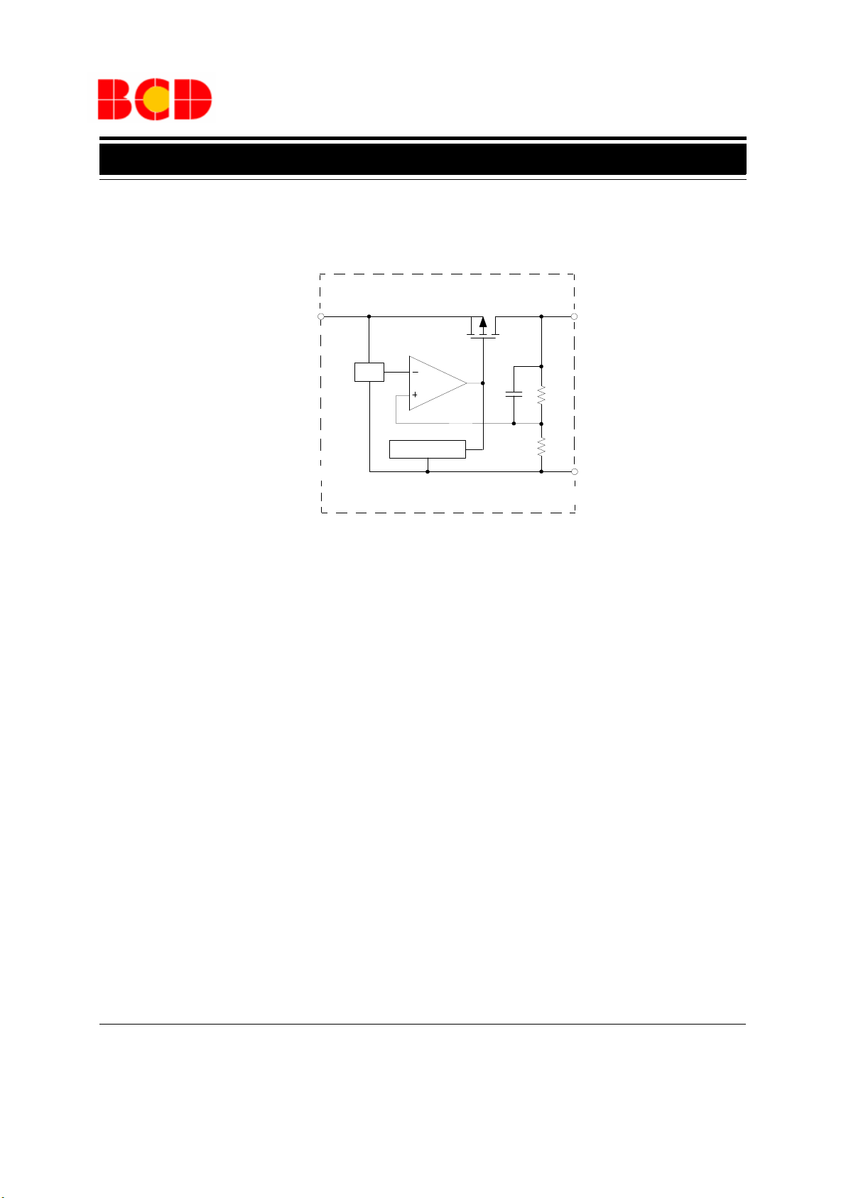
Data Sheet
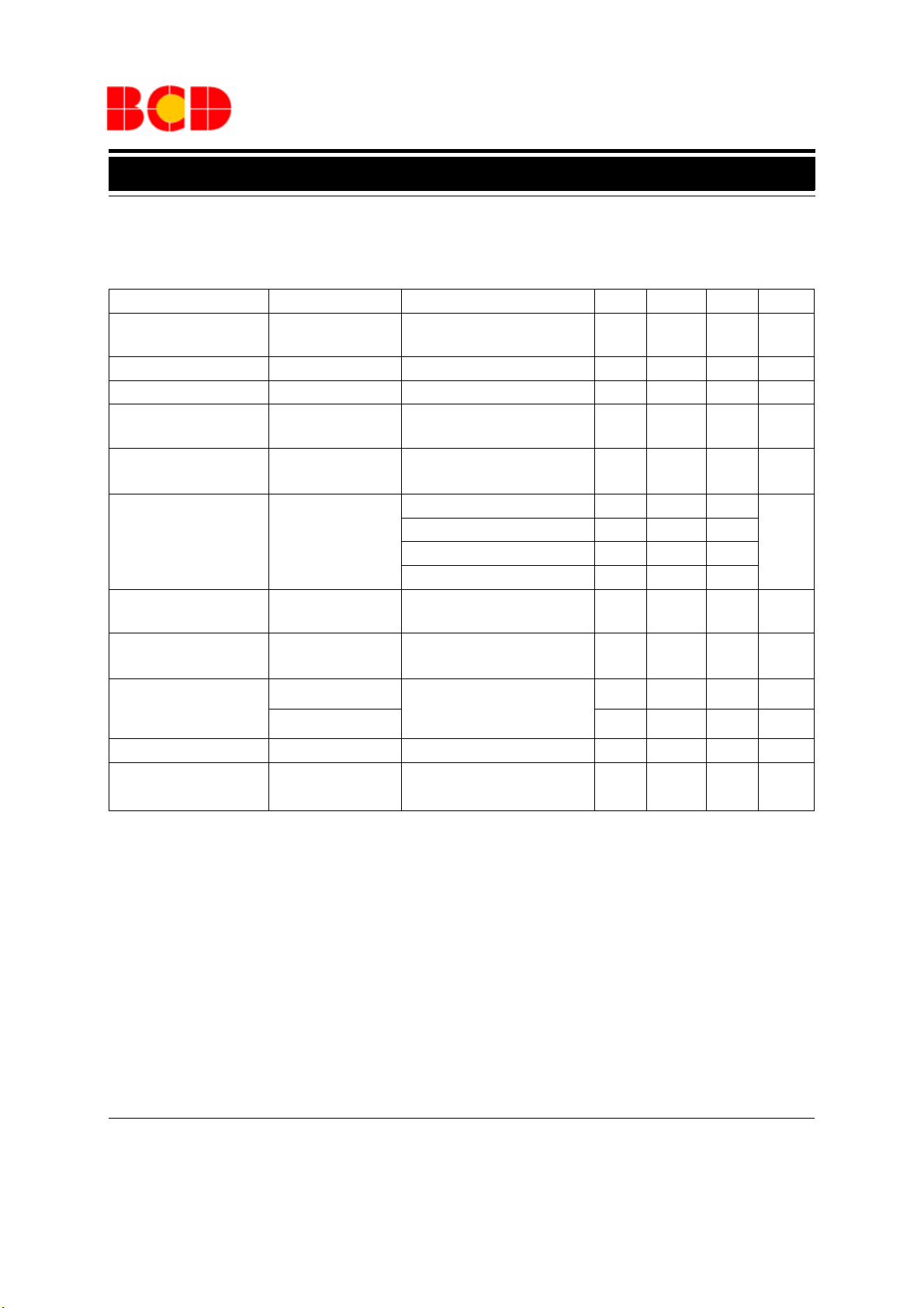
VREF
CURRENT LIMIT
HIGH SPEED, EXTREMELY LOW NOISE LDO REGULATOR AP2120
Functional Block Diagram
3(1){2}
V
IN
2(2){3}
1(3){1}
Figure 3. Functional Block Diagram of AP2120
V
OUT
GND
A(B){C}
A for SOT-23 (N)
B for SOT-23 (NA)
C for SOT-89/TO-92
Mar. 2013 Rev. 1. 4 BCD Semiconductor Manufacturing Limited
3
Page 4
Data Sheet
HIGH SPEED, EXTREMELY LOW NOISE LDO REGULATOR AP2120
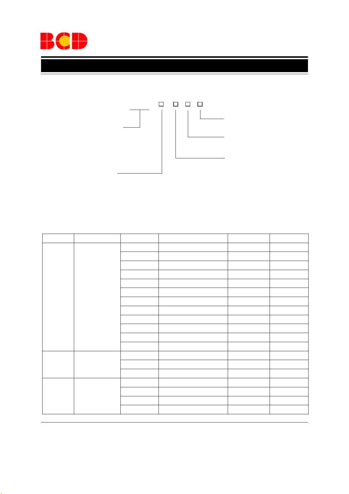
Ordering Information
AP2120 -
G1: Green
Circuit Type
TR: Tape and Reel or Ammo
Package
N/NA: SOT-23
R: SOT-89
Z: TO-92
Blank: Bulk
1.2: Fixed Output 1.2V
1.3: Fixed Output 1.3V
1.5: Fixed Output 1.5V
1.8: Fixed Output 1.8V
2.5: Fixed Output 2.5V
2.8: Fixed Output 2.8V
3.0: Fixed Output 3.0V
3.2: Fixed Output 3.2V
3.3: Fixed Output 3.3V
3.6: Fixed Output 3.6V
4.0: Fixed Output 4.0V
5.0: Fixed Output 5.0V
Package Temperature Range Output Voltage Part Number Marking ID Packing Type
1.2V(N) AP2120N-1.2TRG1 GR4 Tape & Reel
1.3V(N) AP2120N-1.3TRG1 GR5 Tape & Reel
1.5V(N) AP2120N-1.5TRG1 GR6 Tape & Reel
1.8V(N) AP2120N-1.8TRG1 GR7 Tape & Reel
2.5V(N) AP2120N-2.5TRG1 GR8 Tape & Reel
SOT-23
SOT-23
SOT-89
-40 to 85
-40 to 85
-40 to 85
o
C
o
C
o
C
2.8V(N) AP2120N-2.8TRG1 GR9 Tape & Reel
3.0V(N) AP2120N-3.0TRG1 GS2 Tape & Reel
3.2V(N) AP2120N-3.2TRG1 GS3 Tape & Reel
3.3V(N) AP2120N-3.3TRG1 GS4 Tape & Reel
3.6V(N) AP2120N-3.6TRG1 GZ8 Tape & Reel
4.0V(N) AP2120N-4.0TRG1 GZ9 Tape & Reel
5.0V(N) AP2120N-5.0TRG1 GS5 Tape & Reel
3.3V(NA) AP2120NA-3.3TRG1 GZ1 Tape & Reel
3.6V(NA) AP2120NA-3.6TRG1 GAA Tape & Reel
4.0V(NA) AP2120NA-4.0TRG1 GBA Tape & Reel
1.2V AP2120R-1.2TRG1 G13Q Tape & Reel
1.3V AP2120R-1.3TRG1 G17Q Tape & Reel
1.5V AP2120R-1.5TRG1 G22Q Tape & Reel
1.8V AP2120R-1.8TRG1 G27Q Tape & Reel
Mar. 2013 Rev. 1. 4 BCD Semiconductor Manufacturing Limited
4
Page 5
Data Sheet
HIGH SPEED, EXTREMELY LOW NOISE LDO REGULATOR AP2120
Ordering Information (Continued)
Package Temperature Range Output Voltage Part Number Marking ID Packing Type
2.5V AP2120R-2.5TRG1 G28Q Tape & Reel
2.8V AP2120R-2.8TRG1 G31Q Tape & Reel
3.0V AP2120R-3.0TRG1 G33Q Tape & Reel
SOT-89
TO-92
-40 to 85
-40 to 85
o
C
o
C
3.2V AP2120R-3.2TRG1 G37Q Tape & Reel
3.3V AP2120R-3.3TRG1 G41Q Tape & Reel
3.6V AP2120R-3.6TRG1 G42Q Tape & Reel
4.0V AP2120R-4.0TRG1 G43Q Tape & Reel
5.0V AP2120R-5.0TRG1 G70Q Tape & Reel
1.2V AP2120Z-1.2G1 2120Z-1.2G1 Bulk
1.2V AP2120Z-1.2TRG1 2120Z-1.2G1 Ammo
1.3V AP2120Z-1.3G1 2120Z-1.3G1 Bulk
1.3V AP2120Z-1.3TRG1 2120Z-1.3G1 Ammo
1.5V AP2120Z-1.5G1 2120Z-1.5G1 Bulk
1.5V AP2120Z-1.5TRG1 2120Z-1.5G1 Ammo
1.8V AP2120Z-1.8G1 2120Z-1.8G1 Bulk
1.8V AP2120Z-1.8TRG1 2120Z-1.8G1 Ammo
2.5V AP2120Z-2.5G1 2120Z-2.5G1 Bulk
2.5V AP2120Z-2.5TRG1 2120Z-2.5G1 Ammo
2.8V AP2120Z-2.8G1 2120Z-2.8G1 Bulk
2.8V AP2120Z-2.8TRG1 2120Z-2.8G1 Ammo
3.0V AP2120Z-3.0G1 2120Z-3.0G1 Bulk
3.0V AP2120Z-3.0TRG1 2120Z-3.0G1 Ammo
3.2V AP2120Z-3.2G1 2120Z-3.2G1 Bulk
3.2V AP2120Z-3.2TRG1 2120Z-3.2G1 Ammo
3.3V AP2120Z-3.3G1 2120Z-3.3G1 Bulk
3.3V AP2120Z-3.3TRG1 2120Z-3.3G1 Ammo
3.6V AP2120Z-3.6G1 2120Z-3.6G1 Bulk
3.6V AP2120Z-3.6TRG1 2120Z-3.6G1 Ammo
4.0V AP2120Z-4.0G1 2120Z-4.0G1 Bulk
4.0V AP2120Z-4.0TRG1 2120Z-4.0G1 Ammo
5.0V AP2120Z-5.0G1 2120Z-5.0G1 Bulk
5.0V AP2120Z-5.0TRG1 2120Z-5.0G1 Ammo
BCD Semiconductor's products, as designated with "G1" suffix in the part number, are RoHS compliant and Green.
Mar. 2013 Rev. 1. 4
BCD Semiconductor Manufacturing Limited
5
Page 6
Data Sheet
HIGH SPEED, EXTREMELY LOW NOISE LDO REGULATOR AP2120
Absolute Maximum Ratings (Note 1)
Parameter Symbol Value Unit
Input Voltage V
Enable Input Voltage V
Output Current I
Junction Temperature T
Storage Temperature Range T
Lead Temperature (Soldering, 10sec) T
LEAD
IN
CE
OUT
J
STG
6.5 V
-0.3 to VIN+0.3 V
300 mA
150
-65 to 150
260
o
o
o
C
C
C
SOT-23 250
Thermal Resistance (Note 2)
θ
JA
SOT-89 165
o
C/W
TO-92 180
ESD (Human Body Model) ESD 2000 V
ESD (Machine Model) ESD 200 V
Note 1: Stresses greater than those listed under "Absolute Maximum Ratings" may cause permanent damage to the device.
These are stress ratings only, and functional operation of the device at these or any other conditions beyond those indicated
under "Recommended Operating Conditions" is not implied. Exposure to "Absolute Maximum Ratings" for extended periods
may affect device reliability.
Note 2: Absolute maximum ratings indicate limits beyond which damage to the component may occur. Electrical specifications do not apply when operating the device outside of its operating ratings. The maximum allowable power dissipation is a
function of the maximum junction temperature, T
perature, T
)/θ
T
A
The maximum allowable power dissipation at any ambient temperature is calculated using: P
A.
Exceeding the maximum allowable power dissipation will result in excessive die temperature.
JA.
the junction-to-ambient thermal resistance, θ
J(max),
and the ambient tem-
JA,
=(T
D(max)
J(max)
-
Recommended Operating Conditions
Parameter Symbol Min Max Unit
Input Voltage V
Operating Junction Temperature Range T
IN
J
Mar. 2013 Rev. 1. 4 BCD Semiconductor Manufacturing Limited
6
26 V
-40 85
o
C
Page 7

Data Sheet
HIGH SPEED, EXTREMELY LOW NOISE LDO REGULATOR AP2120
Electrical Characteristics
AP2120-1.2 Electrical Characteristics
(VIN=2.2V, TJ=25oC, CIN=1μF, C
Parameter Symbol Conditions Min Typ Max Unit
Output Voltage
Input Voltage V
Output Current I
Load Regulation
Line Regulation
V
V
Dropout Voltage
OUT
=1μF,
V
OUT
OUT
RLOAD
RLINE
V
DROP
Bold
typeface applies over -40oC≤TJ≤
VIN=2.2V
1mA≤I
IN
VIN-V
≤30mA
OUT
=1V 150 mA
OUT
VIN=2.2V
OUT
≤80mA
1mA≤I
2.2V≤VIN≤6V
=30mA
I
OUT
I
=10mA 700 900
OUT
I
=100mA 700 900
OUT
=150mA 700 900
I
OUT
I
=200mA 700 900
OUT
85oC,
unless otherwise specified.)
1.176 1.2 1.224 V
12 40 mV
416mV
6V
mV
Quiescent Current
Power Supply
Rejection Ratio
(ΔV
ΔV
OUT/VOUT
Output Voltage
Temperature Coefficient
Short Current Limit I
RMS Output Noise
I
PSRR
OUT
LIMIT
V
NOISE
Q
VIN=2.2V, I
Ripple 0.5Vp-p, f=1kHz
=2.2V
V
IN
/ΔT
I
=30mA
)/ΔT
OUT
V
=0V 50 mA
OUT
TA=25oC, I
OUT
OUT
=0mA
=0
25 50
μA
65 dB
±120
±100
15
μV/
ppm/
μVrm s
o
C
o
C
10Hz ≤f≤100kHz
Mar. 2013 Rev. 1. 4
BCD Semiconductor Manufacturing Limited
7
Page 8
Data Sheet
HIGH SPEED, EXTREMELY LOW NOISE LDO REGULATOR AP2120
Electrical Characteristics (Continued)
AP2120-1.3 Electrical Characteristics
(VIN=2.3V, TJ=25oC, CIN=1μF, C
Parameter Symbol Conditions Min Typ Max Unit
Output Voltage
Input Voltage V
Output Current I
Load Regulation
Line Regulation
Dropout Voltage
OUT
V
V
=1μF,
V
OUT
OUT
RLOAD
RLINE
V
DROP
Bold
typeface applies over -40oC≤TJ≤
VIN=2.3V
1mA≤I
IN
VIN-V
≤30mA
OUT
=1V 150 mA
OUT
VIN=2.3V
OUT
≤80mA
1mA≤I
2.3V≤VIN≤6V
=30mA
I
OUT
I
=10mA 600 800
OUT
I
=100mA 600 800
OUT
=150mA 600 800
I
OUT
I
=200mA 600 800
OUT
85oC,
unless otherwise specified.)
1.274 1.3 1.326 V
12 40 mV
416mV
6V
mV
Quiescent Current
Power Supply
Rejection Ratio
(ΔV
ΔV
OUT/VOUT
Output Voltage
Temperature Coefficient
Short Current Limit I
RMS Output Noise
I
PSRR
OUT
LIMIT
V
NOISE
Q
VIN=2.3V, I
Ripple 0.5Vp-p, f=1kHz
=2.3V
V
IN
/ΔT
I
=30mA
)/ΔT
OUT
V
=0V 50 mA
OUT
TA=25oC, I
OUT
OUT
=0mA
=0
25 50
μA
65 dB
±130
±100
15
μV/
ppm/
μVrms
o
C
o
C
10Hz ≤f≤100kHz
Mar. 2013 Rev. 1. 4 BCD Semiconductor Manufacturing Limited
8
Page 9

Data Sheet
HIGH SPEED, EXTREMELY LOW NOISE LDO REGULATOR AP2120
Electrical Characteristics (Continued)
AP2120-1.5 Electrical Characteristics
(VIN=2.5V, TJ=25oC, CIN=1μF, C
Parameter Symbol Conditions Min Typ Max Unit
Output Voltage
Input Voltage V
Output Current I
Load Regulation
Line Regulation
V
V
Dropout Voltage
OUT
=1μF,
V
OUT
OUT
RLOAD
RLINE
V
DROP
Bold
typeface applies over -40oC≤TJ≤
VIN=2.5V
1mA≤I
IN
VIN-V
≤30mA
OUT
=1V 150 mA
OUT
VIN=2.5V
OUT
≤80mA
1mA≤I
2.3V≤VIN≤6V
=30mA
I
OUT
I
=10mA 400 600
OUT
I
=100mA 400 600
OUT
=150mA 400 600
I
OUT
I
=200mA 400 600
OUT
85oC,
unless otherwise specified.)
1.47 1.5 1.53 V
12 40 mV
416mV
6V
mV
Quiescent Current
Power Supply
Rejection Ratio
(ΔV
ΔV
OUT/VOUT
Output Voltage
Temperature Coefficient
Short Current Limit I
RMS Output Noise
I
PSRR
OUT
LIMIT
V
NOISE
Q
VIN=2.5V, I
Ripple 0.5Vp-p, f=1kHz
=2.5V
V
IN
/ΔT
I
=30mA
)/ΔT
OUT
V
=0V 50 mA
OUT
TA=25oC, I
OUT
OUT
=0mA
=0
25 50
μA
65 dB
±150
±100
15
μV/
ppm/
μVrm s
o
C
o
C
10Hz ≤f≤100kHz
Mar. 2013 Rev. 1. 4
BCD Semiconductor Manufacturing Limited
9
Page 10

Data Sheet
HIGH SPEED, EXTREMELY LOW NOISE LDO REGULATOR AP2120
Electrical Characteristics (Continued)
AP2120-1.8 Electrical Characteristics
(VIN=2.8V, TJ=25oC, CIN=1μF, C
Parameter Symbol Conditions Min Typ Max Unit
Output Voltage
Input Voltage V
Output Current I
Load Regulation
Line Regulation
Dropout Voltage
OUT
V
V
=1μF,
V
OUT
OUT
RLOAD
RLINE
V
DROP
Bold
typeface applies over -40oC≤TJ≤
VIN=2.8V
1mA≤I
IN
VIN-V
≤30mA
OUT
=1V 150 mA
OUT
VIN=2.8V
OUT
≤80mA
1mA≤I
2.3V≤VIN≤6V
=30mA
I
OUT
I
=10mA 20 40
OUT
=100mA 200 300
I
OUT
=150mA 300 500
I
OUT
85oC,
unless otherwise specified.)
1.764 1.8 1.836 V
12 40 mV
416mV
6V
mV
Quiescent Current
Power Supply
Rejection Ratio
(ΔV
ΔV
OUT/VOUT
Output Voltage
Temperature Coefficient
Short Current Limit I
RMS Output Noise
I
PSRR
OUT
LIMIT
V
NOISE
Q
VIN=2.8V, I
Ripple 0.5Vp-p, f=1kHz
=2.8V
V
IN
/ΔT
I
=30mA
)/ΔT
OUT
V
=0V 50 mA
OUT
TA=25oC
10Hz ≤f≤100kHz
OUT
=0mA
25 50
μA
65 dB
±180
±100
30
μV/
ppm/
μVrms
o
C
o
C
Mar. 2013 Rev. 1. 4 BCD Semiconductor Manufacturing Limited
10
Page 11

Data Sheet
HIGH SPEED, EXTREMELY LOW NOISE LDO REGULATOR AP2120
Electrical Characteristics (Continued)
AP2120-2.5 Electrical Characteristics
(VIN=3.5V, TJ=25oC, CIN=1μF, C
Parameter Symbol Conditions Min Typ Max Unit
Output Voltage
Input Voltage V
Output Current I
Load Regulation
Line Regulation
Dropout Voltage
OUT
V
V
=1μF,
V
OUT
IN
OUT
RLOAD
RLINE
V
DROP
Bold
typeface applies over -40oC≤TJ≤
VIN=3.5V
1mA≤I
VIN-V
≤30mA
OUT
=1V 150 mA
OUT
VIN=3.5V
OUT
≤80mA
1mA≤I
3V≤VIN≤6V
=30mA
I
OUT
I
=10mA 20 40
OUT
=100mA 200 300
I
OUT
=150mA 300 500
I
OUT
85oC,
unless otherwise specified.)
2.45 2.5 2.55 V
12 40 mV
416mV
6V
mV
Quiescent Current
Power Supply
Rejection Ratio
(ΔV
ΔV
OUT/VOUT
Output Voltage
Temperature Coefficient
Short Current Limit I
RMS Output Noise
I
PSRR
OUT
LIMIT
V
NOISE
Q
VIN=3.5V, I
Ripple 0.5Vp-p, f=1kHz
=3.5V
V
IN
/ΔT
I
=30mA
)/ΔT
OUT
V
=0V 50 mA
OUT
TA=25oC
10Hz ≤f≤100kHz
OUT
=0mA
25 50
μA
65 dB
±250
±100
30
μV/
ppm/
μVrm s
o
C
o
C
Mar. 2013 Rev. 1. 4
BCD Semiconductor Manufacturing Limited
11
Page 12

Data Sheet
HIGH SPEED, EXTREMELY LOW NOISE LDO REGULATOR AP2120
Electrical Characteristics (Continued)
AP2120-2.8 Electrical Characteristics
(VIN=3.8V, TJ=25oC, CIN=1μF, C
Parameter Symbol Conditions Min Typ Max Unit
Output Voltage
Input Voltage V
Output Current I
Load Regulation
Line Regulation
Dropout Voltage
OUT
V
V
=1μF,
V
OUT
OUT
RLOAD
RLINE
V
DROP
Bold
typeface applies over -40oC≤TJ≤
VIN=3.8V
1mA≤I
IN
VIN-V
≤30mA
OUT
=1V 150 mA
OUT
VIN=3.8V
OUT
≤80mA
1mA≤I
3.3V≤VIN≤6V
=30mA
I
OUT
I
=10mA 20 40
OUT
=100mA 200 300
I
OUT
=150mA 300 500
I
OUT
85oC,
unless otherwise specified.)
2.744 2.8 2.856 V
12 40 mV
416mV
6V
mV
Quiescent Current
Power Supply
Rejection Ratio
(ΔV
ΔV
OUT/VOUT
Output Voltage
Temperature Coefficient
Short Current Limit I
RMS Output Noise
I
PSRR
OUT
LIMIT
V
NOISE
Q
VIN=3.8V, I
Ripple 0.5Vp-p, f=1kHz
=3.8V
V
IN
/ΔT
I
=30mA
)/ΔT
OUT
V
=0V 50 mA
OUT
TA=25oC
10Hz ≤f≤100kHz
OUT
=0mA
25 50
μA
65 dB
±280
±100
30
μV/
ppm/
μVrm s
o
C
o
C
Mar. 2013 Rev. 1. 4 BCD Semiconductor Manufacturing Limited
12
Page 13

Data Sheet
HIGH SPEED, EXTREMELY LOW NOISE LDO REGULATOR AP2120
Electrical Characteristics (Continued)
AP2120-3.0 Electrical Characteristics
(VIN=4V, TJ=25oC, CIN=1μF, C
Parameter Symbol Conditions Min Typ Max Unit
Output Voltage
Input Voltage V
Output Current I
Load Regulation
Line Regulation
Dropout Voltage
=1μF,
OUT
V
V
V
OUT
OUT
RLOAD
RLINE
V
DROP
Bold
typeface applies over -40oC≤TJ≤
VIN=4V
1mA≤I
OUT
IN
VIN-V
=1V 150 mA
OUT
VIN=4V
1mA≤I
OUT
3.5V≤VIN≤6V
=30mA
I
OUT
I
=10mA 20 40
OUT
=100mA 200 300
I
OUT
I
=150mA 300 500
OUT
≤30mA
≤80mA
85oC,
unless otherwise specified.)
2.94 3.0 3.06 V
12 40 mV
416mV
6V
mV
Quiescent Current
Power Supply
Rejection Ratio
(ΔV
ΔV
OUT/VOUT
Output Voltage
Temperature Coefficient
Short Current Limit I
RMS Output Noise
I
PSRR
OUT
LIMIT
V
NOISE
Q
VIN=4V, I
Ripple 0.5Vp-p, f=1kHz
=4V
V
IN
/ΔT
I
=30mA
)/ΔT
OUT
V
=0V 50 mA
OUT
TA=25oC
OUT
=0mA
25 50
μA
65 dB
±300
±100
30
μV/
ppm/
μVrms
o
C
o
C
10Hz ≤f≤100kHz
Mar. 2013 Rev. 1. 4
BCD Semiconductor Manufacturing Limited
13
Page 14

Data Sheet
HIGH SPEED, EXTREMELY LOW NOISE LDO REGULATOR AP2120
Electrical Characteristics (Continued)
AP2120-3.2 Electrical Characteristics
(VIN=4.2V, TJ=25oC, CIN=1μF, C
Parameter Symbol Conditions Min Typ Max Unit
Output Voltage
Input Voltage V
Output Current I
Load Regulation
Line Regulation
Dropout Voltage
OUT
V
V
=1μF,
V
OUT
IN
OUT
RLOAD
RLINE
V
DROP
Bold
typeface applies over -40oC≤TJ≤
VIN=4.2V
1mA≤I
VIN-V
≤30mA
OUT
=1V 150 mA
OUT
VIN=4.2V
OUT
≤ 80mA
1mA≤ I
3.7V≤VIN≤6V
=30mA
I
OUT
I
=10mA 20 40
OUT
=100mA 200 300
I
OUT
=150mA 300 500
I
OUT
85oC,
unless otherwise specified.)
3.136 3.2 3.264 V
12 40 mV
416mV
6V
mV
Quiescent Current
Power Supply
Rejection Ratio
(ΔV
ΔV
OUT/VOUT
Output Voltage
Temperature Coefficient
Short Current Limit I
RMS Output Noise
I
PSRR
OUT
LIMIT
V
NOISE
Q
VIN=4.2V, I
Ripple 0.5Vp-p, f=1kHz
=4.2V
V
IN
/ΔT
I
=30mA
)/ΔT
OUT
V
=0V 50 mA
OUT
TA=25oC
10Hz ≤f≤100kHz
OUT
=0mA
25 50
μA
65 dB
±320
±100
30
μV/
ppm/
μVrms
o
C
o
C
Mar. 2013 Rev. 1. 4 BCD Semiconductor Manufacturing Limited
14
Page 15

Data Sheet
HIGH SPEED, EXTREMELY LOW NOISE LDO REGULATOR AP2120
Electrical Characteristics (Continued)
AP2120-3.3 Electrical Characteristics
(VIN=4.3V, TJ=25oC, CIN=1μF, C
Parameter Symbol Conditions Min Typ Max Unit
Output Voltage
Input Voltage V
Output Current I
Load Regulation
Line Regulation
Dropout Voltage
OUT
V
V
=1μF,
V
OUT
IN
OUT
RLOAD
RLINE
V
DROP
Bold
typeface applies over -40oC≤TJ≤
VIN=4.3V
1mA≤I
VIN-V
≤30mA
OUT
=1V 150 mA
OUT
VIN=4.3V
OUT
≤ 80mA
1mA≤ I
3.8V≤VIN≤6V
=30mA
I
OUT
I
=10mA 20 40
OUT
=100mA 200 300
I
OUT
=150mA 300 500
I
OUT
85oC,
unless otherwise specified.)
3.234 3.3 3.366 V
12 40 mV
416mV
6V
mV
Quiescent Current
Power Supply
Rejection Ratio
(ΔV
ΔV
OUT/VOUT
Output Voltage
Temperature Coefficient
Short Current Limit I
RMS Output Noise
I
PSRR
OUT
LIMIT
V
NOISE
Q
VIN=4.3V, I
Ripple 0.5Vp-p, f=1kHz
=4.3V
V
IN
/ΔT
I
=30mA
)/ΔT
OUT
V
=0V 50 mA
OUT
TA=25oC
10Hz ≤f≤100kHz
OUT
=0mA
25 50
μA
65 dB
±330
±100
30
μV/
ppm/
μVrms
o
C
o
C
Mar. 2013 Rev. 1. 4
BCD Semiconductor Manufacturing Limited
15
Page 16

Data Sheet
HIGH SPEED, EXTREMELY LOW NOISE LDO REGULATOR AP2120
Electrical Characteristics (Continued)
AP2120-3.6 Electrical Characteristics
(VIN=4.6V, TJ=25oC, CIN=1μF, C
Parameter Symbol Conditions Min Typ Max Unit
Output Voltage
Input Voltage V
Output Current I
Load Regulation
Line Regulation
Dropout Voltage
OUT
V
V
=1μF,
V
OUT
IN
OUT
RLOAD
RLINE
V
DROP
Bold
typeface applies over -40oC≤TJ≤
VIN=4.6V
1mA≤I
VIN-V
≤30mA
OUT
=1V 150 mA
OUT
VIN=4.6V
OUT
≤ 80mA
1mA≤ I
4.6V≤VIN≤6V
=30mA
I
OUT
I
=10mA 20 40
OUT
=100mA 200 300
I
OUT
I
=150mA 300 500
OUT
85oC,
unless otherwise specified.)
3.528 3.6 3.672 V
12 40 mV
416mV
6V
mV
Quiescent Current
Power Supply
Rejection Ratio
(ΔV
ΔV
OUT/VOUT
Output Voltage
Temperature Coefficient
Short Current Limit I
RMS Output Noise
I
PSRR
OUT
LIMIT
V
NOISE
Q
VIN=4.6V, I
Ripple 0.5Vp-p, f=1kHz
=4.6V
V
IN
/ΔT
I
=30mA
)/ΔT
OUT
V
=0V 50 mA
OUT
TA=25oC
OUT
=0mA
25 50
μA
65 dB
±330
±100
30
μV/
ppm/
μVrms
o
C
o
C
10Hz ≤f≤100kHz
Mar. 2013 Rev. 1. 4 BCD Semiconductor Manufacturing Limited
16
Page 17

Data Sheet
HIGH SPEED, EXTREMELY LOW NOISE LDO REGULATOR AP2120
Electrical Characteristics (Continued)
AP2120-4.0 Electrical Characteristics
(VIN=5.0V, TJ=25oC, CIN=1μF, C
Parameter Symbol Conditions Min Typ Max Unit
Output Voltage
Input Voltage V
Output Current I
Load Regulation
Line Regulation
Dropout Voltage
OUT
V
V
=1μF,
V
OUT
IN
OUT
RLOAD
RLINE
V
DROP
Bold
typeface applies over -40oC≤TJ≤
VIN=5.0V
1mA≤I
VIN-V
≤30mA
OUT
=1V 150 mA
OUT
VIN=5.0V
OUT
≤ 80mA
1mA≤ I
5V≤VIN≤6V
=30mA
I
OUT
I
=10mA 20 40
OUT
I
=100mA 200 300
OUT
=150mA 300 500
I
OUT
85oC,
unless otherwise specified.)
3.92 4.0 4.08 V
12 40 mV
416mV
6V
mV
Quiescent Current
Power Supply
Rejection Ratio
(ΔV
ΔV
OUT/VOUT
Output Voltage
Temperature Coefficient
Short Current Limit I
RMS Output Noise
I
PSRR
OUT
LIMIT
V
NOISE
Q
VIN=5.0V, I
Ripple 0.5Vp-p, f=1kHz
=5.0V
V
IN
/ΔT
I
=30mA
)/ΔT
OUT
V
=0V 50 mA
OUT
TA=25oC
OUT
=0mA
25 50
μA
65 dB
±330
±100
30
μV/
ppm/
μVrm s
o
C
o
C
10Hz ≤f≤100kHz
Mar. 2013 Rev. 1. 4
BCD Semiconductor Manufacturing Limited
17
Page 18

Data Sheet
HIGH SPEED, EXTREMELY LOW NOISE LDO REGULATOR AP2120
Electrical Characteristics (Continued)
AP2120-5.0 Electrical Characteristics
(VIN=6.0V, TJ=25oC, CIN=1μF, C
Parameter Symbol Conditions Min Typ Max Unit
Output Voltage
Input Voltage V
Output Current I
Load Regulation
Line Regulation
Dropout Voltage
OUT
V
V
=1μF,
V
OUT
IN
OUT
RLOAD
RLINE
V
DROP
Bold
typeface applies over -40oC≤TJ≤
VIN=6.0V
1mA≤I
VIN-V
≤30mA
OUT
=1V 150 mA
OUT
VIN=4.3V
OUT
≤ 80mA
1mA≤ I
5.5V≤VIN≤6V
=30mA
I
OUT
I
=10mA 20 40
OUT
=100mA 200 300
I
OUT
=150mA 300 500
I
OUT
85oC,
unless otherwise specified.)
4.9 5.0 5.1 V
12 40 mV
416mV
6V
mV
Quiescent Current
Power Supply
Rejection Ratio
(ΔV
ΔV
OUT/VOUT
Output Voltage
Temperature Coefficient
Short Current Limit I
RMS Output Noise
I
PSRR
OUT
LIMIT
V
NOISE
Q
VIN=6.0V, I
Ripple 0.5Vp-p, f=1kHz
=6.0V
V
IN
/ΔT
I
=30mA
)/ΔT
OUT
V
=0V 50 mA
OUT
TA=25oC
10Hz ≤f≤100kHz
OUT
=0mA
25 50
μA
65 dB
±330
±100
30
μV/
ppm/
μVrms
o
C
o
C
Mar. 2013 Rev. 1. 4 BCD Semiconductor Manufacturing Limited
18
Page 19
Data Sheet
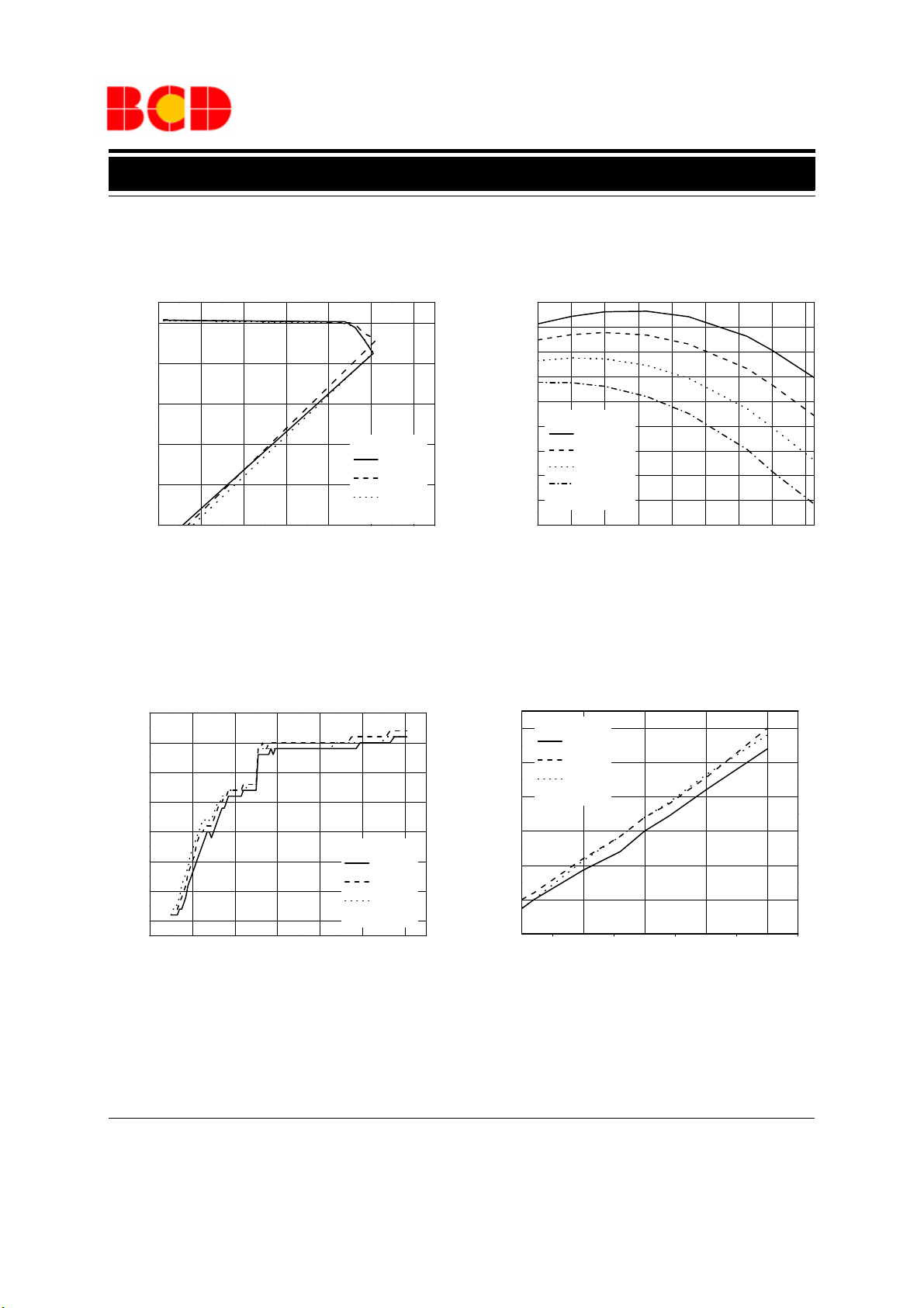
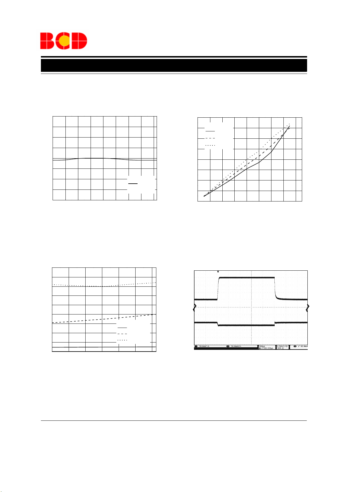
0.00 0.05 0.10 0.15 0.20 0.25 0.30
0.0
0.5
1.0
1.5
2.0
2.5
Output Voltage (V)
Output Current (A)
AP2120-2.5
TC=-40oC
TC=25oC
TC=85oC
V
IN
=3.5V
-40-20 0 20406080100120
2.490
2.495
2.500
2.505
2.510
2.515
2.520
2.525
2.530
2.535
Output Voltage (V)
Case Temperature (oC)
AP2120-2.5
I
OUT
=10mA
I
OUT
=50mA
I
OUT
=100mA
I
OUT
=150mA
V
IN
=3.5V
0123456
0
5
10
15
20
25
30
35
Quiescent Current (μA)
Input Voltage (V)
AP2120-2.5
TC=-40oC
TC=25oC
TC=85oC
I
OUT
=0
0.00 0.05 0.10 0.15 0.20
25
30
35
40
45
50
55
Quiescent Current (μA)
Output Current (A)
AP2120-2.5
TC=-40oC
TC=25oC
TC=85oC
V
IN
=3.5V
HIGH SPEED, EXTREMELY LOW NOISE LDO REGULATOR AP2120
Typical Performance Characteristics
Figure 4. Output Voltage vs. Output Current
Figure 6. Quiescent Current vs. Input Voltage
Mar. 2013 Rev. 1. 4
Figure 5. Output Voltage vs. Case Temperature
Figure 7. Quiescent Current vs. Output Current
BCD Semiconductor Manufacturing Limited
19
Page 20
Data Sheet
-40-20 0 20406080100120
10
15
20
25
30
35
40
45
50
Quiescent Current (μA)
Case Temperature (oC)
AP2120-2.5
VIN=3.5V
I
OUT
=0
0.00 0.02 0.04 0.06 0.08 0.10 0.12 0.14 0.16
0
50
100
150
200
250
300
350
400
Dropout Voltage (V)
Output Current (A)
AP2120-2.5
TC=-40oC
TC=25oC
TC=85oC
-40 -20 0 20 40 60 80
0
50
100
150
200
250
300
350
400
450
Dropout Voltage (V)
Case Temperature (oC)
AP2120-2.5
I
OUT
=10mA
I
OUT
=80mA
I
OUT
=150mA
HIGH SPEED, EXTREMELY LOW NOISE LDO REGULATOR AP2120
Typical Performance Characteristics (Continued)
Figure 8. Quiescent Current vs. Case Temperature
Figure 10. Dropout Voltage vs. Case Temperature
Mar. 2013 Rev. 1. 4 BCD Semiconductor Manufacturing Limited
Figure 9. Dropout Voltage vs. Output Current
150
100
50
(5 0m A/ Di v)
0
OUT
I
50
0
-50
(50mV/Div)
-100
OUT
V
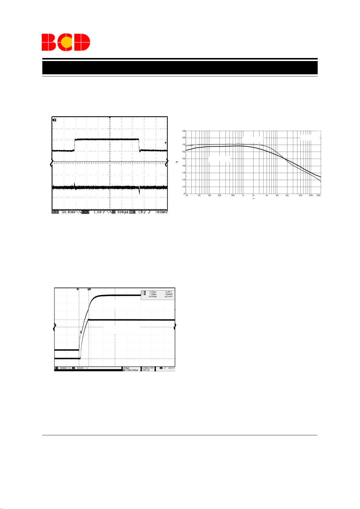
Figure 11. Load Transient (I
OUT
AP2120-2.5
=0 to 150mA)
20
Page 21
Data Sheet
HIGH SPEED, EXTREMELY LOW NOISE LDO REGULATOR AP2120
Typical Performance Characteristics (Continued)
2
1
( 1 V / D i v )
IN
V
0
50
(50mV/Div)
0
OUT
-50
V
Figure 12. Line Transient
(Condition:VIN=2.5V to 3.5,I
3.5
3.0
2.5
2.0
1.5
1.0
(0.5V/Div)
0.5
IN
V
0
Input Voltage
Output Voltage
AP2120-2.5
=10mA)
OUT
AP2120-2.5
3.0
2.5
2.0
1.5
1.0
0.5
0
(0.5V/Div)
OUT
V
=10mA
I
OUT
I
=150mA
OUT
Figure 13. PSRR vs. Frequency
AP2120-2.5
Figure 14. Start-up
Mar. 2013 Rev. 1. 4
BCD Semiconductor Manufacturing Limited
21
Page 22
Data Sheet
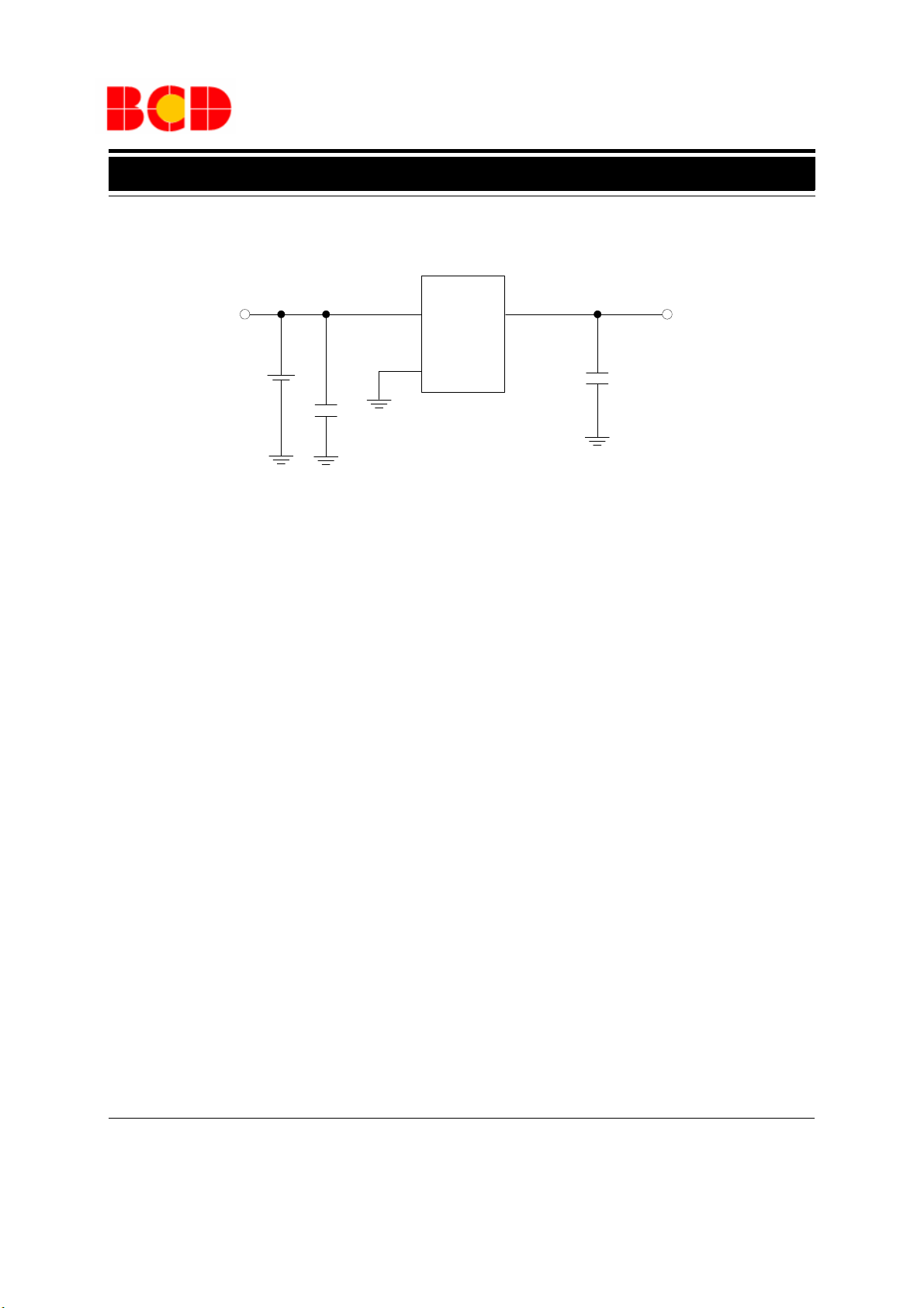
V
IN
AP2120-2.5
C
IN
1μF
C
OUT
1μF
V
OUT
V
IN
V
OUT
GND
VIN=3.5V
V
OUT
=2.5V
HIGH SPEED, EXTREMELY LOW NOISE LDO REGULATOR AP2120
Typical Application
Note: Filter capacitors are required at the AP2120's input and output. 1μF capacitor is required at the input. The
minimum output capacitance required for stability should be more than 1μF with ESR from 0.01Ω to 100Ω.
Ceramic capacitors are recommended.
Figure 15. Typical Application of AP2120
Mar. 2013 Rev. 1. 4 BCD Semiconductor Manufacturing Limited
22
Page 23
Data Sheet
2.300(0.091)
2.500(0.098)
1.200(0.047)
1.400(0.055)
0.890(0.035)
1.030(0.041)
0.300(0.012)
0.510(0.020)
1.900(0.075)REF
2.800(0.110)
3.000(0.118)
2.0°
3.0 °
0.500(0.020)
0.700(0.028)
1.050(0.041)REF
0.010(0.0004)
0.100(0.004)
0.900(0.035)
1.100(0.043)
4×
R0.100(0.004)
7.0°
7.0°
0.550(0.022)REF
0.200(0.008)MIN
0.100(0.004) GAUGE PLANE
0.080(0.003)
0.180(0.007)
R0.100(0.004)
0.0°~10.0°
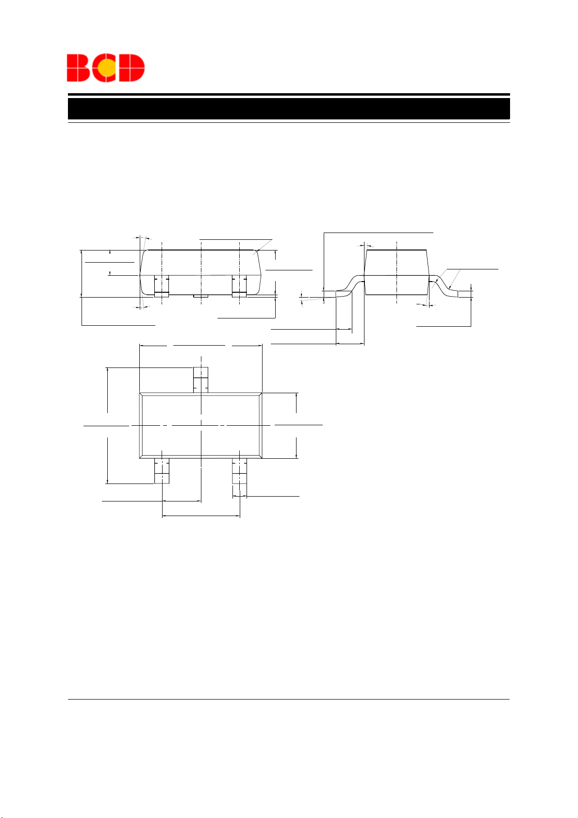
HIGH SPEED, EXTREMELY LOW NOISE LDO REGULATOR AP2120
Mechanical Dimensions
SOT-23 Unit: mm(inch)
Mar. 2013 Rev. 1. 4
BCD Semiconductor Manufacturing Limited
23
Page 24
Data Sheet
45
1.030(0.041)REF
1.550(0.061)REF
4.400(0.173)
4.600(0.181)
0.900(0.035)
1.100(0.043)
3.950(0.156)
4.250(0.167)
3.000(0.118)
TYP
0.480(0.019)
2.300(0.091)
2.600(0.102)
0.320(0.013)
0.520(0.020)
3
10
2.060(0.081)REF
1.400(0.055)
1.600(0.063)
0.350(0.014)
0.450(0.018)
R0.150(0.006)
3
10
1.500(0.059)
0.320(0.013)REF
1.620(0.064)REF
2.210(0.087)REF
0.320(0.013)
0.520(0.020)
1.800(0.071)
HIGH SPEED, EXTREMELY LOW NOISE LDO REGULATOR AP2120
Mechanical Dimensions (Continued)
SOT-89
Unit: mm(inch)
Mar. 2013 Rev. 1. 4 BCD Semiconductor Manufacturing Limited
24
Page 25
Data Sheet
2.420(0.095)
2.660(0.105)
0.360(0.014)
0.760(0.030)
Φ
1.600(0.063)
MAX
12.500(0.492)
15.500(0.610)
1.270(0.050)
TYP
3.300(0.130)
3.700(0.146)
4.300(0.169)
4.700(0.185)
1.000(0.039)
1.400(0.055)
4.400(0.173)
4.800(0.189)
3.430(0.135)
MIN
0.320(0.013)
0.510(0.020)
0.000(0.000)
0.380(0.015)
HIGH SPEED, EXTREMELY LOW NOISE LDO REGULATOR AP2120
Mechanical Dimensions (Continued)
TO-92 (Bulk Packing)
Unit: mm(inch)
Mar. 2013 Rev. 1. 4
BCD Semiconductor Manufacturing Limited
25
Page 26

Data Sheet
4.300(0.169)
4.700(0.185)
1
2.500(0.492)14.500(0.571)
2.540(0. 100
)
Ty
p
1.270(0.050
)
Typ
0. (0. 015)
0.
550
(0.022
)
4.400(0. 173
)
4.
800
(
0.
189
)
3.430(0.135
)
MIN
0.320(0.013
)
0
. 510(0. 020)
0.000(0.000
)
0.380(0.015
)
MAX
1. 100(0. 043
1.400(0.055
)
3.300(0.130)
3.800(0.150)
Φ
1.600(0.063)
)
380
2.500(0. 098
)
4.000(0.157
)
13. 000(0.512
)
15.000(0.591
)
HIGH SPEED, EXTREMELY LOW NOISE LDO REGULATOR AP2120
Mechanical Dimensions (Continued)
TO-92 (Ammo Packing)
Unit: mm(inch)
Mar. 2013 Rev. 1. 4 BCD Semiconductor Manufacturing Limited
26
Page 27

BCD Semiconductor Manufacturing Limited
IMPORTANT NOTICE
http://www.bcdsemi.com
BCD Semiconductor Manufacturing Limited reserves the right to make changes without further notice to any products or specifications herein. BCD Semiconductor Manufacturing Limited does not assume any responsibility for use of any its products for any
IMPORTANT NOTICE
IMPORTANT NOTICE
particular purpose, nor does BCD Semiconductor Manufacturing Limited assume any liability arising out of the application or use
of any its products or circuits. BCD Semiconductor Manufacturing Limited does not convey any license under its patent rights or
BCD Semiconductor Manufacturing Limited reserves the right to make changes without further notice to any products or specifi-
BCD Semiconductor Manufacturing Limited reserves the right to make changes without further notice to any products or specifi-
other rights nor the rights of others.
cations herein. BCD Semiconductor Manufacturing Limited does not assume any responsibility for use of any its products for any
cations herein. BCD Semiconductor Manufacturing Limited does not assume any responsibility for use of any its products for any
particular purpose, nor does BCD Semiconductor Manufacturing Limited assume any liability arising out of the application or use
particular purpose, nor does BCD Semiconductor Manufacturing Limited assume any liability arising out of the application or use
MAIN SITE
of any its products or circuits. BCD Semiconductor Manufacturing Limited does not convey any license under its patent rights or
of any its products or circuits. BCD Semiconductor Manufacturing Limited does not convey any license under its patent rights or
- Headquarters
BCD (Shanghai) Micro-electronics Limited
other rights nor the rights of others.
other rights nor the rights of others.
No. 1600, Zi Xing Road, Shanghai ZiZhu Science-based Industrial Park, 200241, P. R.C.
Tel: +86-021-2416-2266, Fax: +86-021-2416-2277
MAIN SITE
MAIN SITE
REGIONAL SALES OFFICE
- Headquarters
BCD Semiconductor Manufacturing Limited
BCD Semiconductor Manufactur ing Limited
Shenzhen Office
- Wafer Fab
No. 1600, Zi Xing Road, Shanghai ZiZhu Science-based Industrial Park, 200241, China
Shanghai SIM-BCD Semiconductor Manufacturing Co., Ltd., Shenzhen Office
Shanghai SIM-BCD Semiconductor Manufacturing Limited
Tel: +86-21-24162266, Fax: +86-21-24162277
Unit A Room 1203,Skyworth Bldg., Gaoxin Ave.1.S., Nanshan District
800, Yi Shan Road, Shanghai 200233, China
Shenzhen 518057, China
Tel: +86-21-6485 1491, Fax: +86-21-5450 0008
REGIONAL SALES OFFICE
Tel: +86-0755-8660-4900, Fax: +86-0755-8660-4958
Shenzhen Office
REGIONAL SALES OFFICE
Shanghai SIM-BCD Semiconductor Manufacturing Co., Ltd., Shenzhen Office
Taiwan Office (Hsinchu)
Shenzhen Office
Unit A Room 1203, Skyworth Bldg., Gaoxin Ave.1.S., Nanshan District, Shenzhen,
BCD Semiconductor (Taiwan) Company Limited
Shanghai SIM-BCD Semiconductor Manufacturing Co., Ltd. Shenzhen Office
China
8F, No.176, Sec. 2, Gong-Dao 5th Road, East District
Advanced Analog Circuits (Shanghai) Corporation Shenzhen Office
Tel: +86-755-8826 7951
HsinChu City 300, Taiwan, R.O.C
Room E, 5F, Noble Center, No.1006, 3rd Fuzhong Road, Futian District, Shenzhen 518026, China
Fax: +86-755-8826 7865
Tel: +886-3-5160181, Fax: +886-3-5160181
Tel: +86-755-8826 7951
Fax: +86-755-8826 7865
- Wafer Fab
Shanghai SIM-BCD Semiconductor Manufacturing Co., Ltd.
800 Yishan Road, Shanghai 200233, China
Tel: +021-6485-1491, Fax: +86-021-5450-0008
- Wafer Fab
BCD Semiconductor Manufacturing Limited
Shanghai SIM-BCD Semiconductor Manufacturing Co., Ltd.
Taiwan Office (Taipei)
- IC Design Group
800 Yi Shan Road, Shanghai 200233, China
BCD Semiconductor (Taiwan) Company Limited
Advanced Analog Circuits (Shanghai) Corporation
Tel: +86-21-6485 1491, Fax: +86-21-5450 0008
3F, No.17, Lane 171, Sec. 2, Jiu-Zong Rd., Nei-Hu Dist., Taipei(114), Taiwan, R.O.C
8F, Zone B, 900, Yi Shan Road, Shanghai 200233, China
Tel: +886-2-2656 2808
Tel: +86-21-6495 9539, Fax: +86-21-6485 9673
Fax: +886-2-2656-2806/26562950
Taiwan Office
BCD Semiconductor (Taiwan) Company Limited
USA Office
Taiwan Office
4F, 298-1, Rui Guang Road, Nei-Hu District, Taipei,
BCD Semiconductor Corp.
BCD Semiconductor (Taiwan) Company Limited
Tai wan
48460 Kato Road, Fremont, CA 94538, USA
4F, 298-1, Rui Guang Road, Nei-Hu District, Taipei,
Tel: +886-2-2656 2808
Tel: +1-510-668-1950
Taiwan
Fax: +886-2-2656 2806
Fax: +1-510-668-1990
Tel: +886-2-2656 2808
Fax: +886-2-2656 2806
USA Office
Korea Office
BCD Semiconductor Limited Korea office.
Room 101-1112, Digital-Empire II, 486 Sin-dong,
Yeongtong-Gu, Suwon-city, Gyeonggi-do, Korea
Tel: +82-31-695-8430
BCD Semiconductor Corp.
USA Office
30920 Huntwood Ave. Hayward,
BCD Semiconductor Corporation
CA 94544, USA
30920 Huntwood Ave. Hayward,
Tel : +1-510-324-2988
CA 94544, U.S.A
Fax: +1-510-324-2788
Tel : +1-510-324-2988
Fax: +1-510-324-2788
 Loading...