

Page 1
1.6x Linear DC Fan Driver with VOUT Fully on Control AP2113
Preliminary Datasheet
General Description
The AP2113 is a low dropout high performance linear
regulator which is specially designed to drive a DC
fan, the regulator delivers output current 600mA in
minimum.
The AP2113 provides low quiescent current
consumption 70µA, over current limit protection and
load short current protection with fold-back limitation
50mA, which are ideal for battery powered system
application.
The AP2113 output voltage (V
of V
m
(set FON
larger than 1.0V to guarantee V
An FON
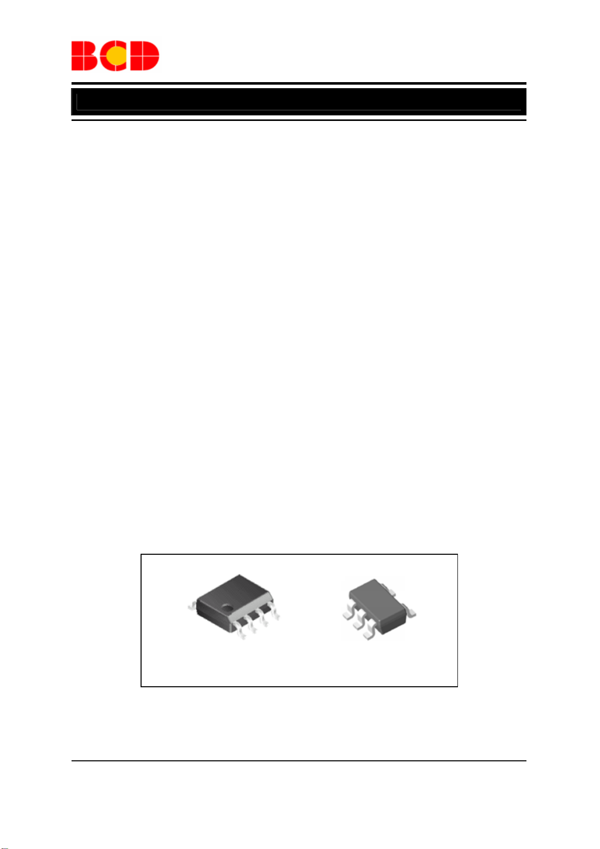
The AP2113 is available in standard SOIC-8 and
SOT-23-5 packages.
input voltage until it reaches VIN voltage
SET
inus dropout voltage (V
________
pin logic high). The V
________
pin turns V
fully on when set logic low.
OUT
) follows 1.6 times
OUT
) at adjustable mode
DROP
voltage must be
SET
1.6 times of V
OUT
SET
Features
• Output Voltage in Adjustable Mode Follows 1.6
Times of V
• Low Quiescent Current: 70µA (Typ)
• Guarantee 0.6A Continuous Load
• Switchable Adjustable Mode/Full Speed Mode
• Over Current Protection
• Short Current Protection with Fold-back
Limitation: 50mA
• Low Dropout Voltage:
150mV @ 600mA (Typ) at Full Speed Mode
200mV @ 600mA (Typ) at Adjustable Mode
• OTSD Protection
• Stable with 1.0µF Flexible Caps: Ceramic,
Tantalum and Aluminum Electrolytic
• Operation Temperature Range: -40°C to 85°C
• ESD: MM 300V, HBM 6000V
.
SET
(V
OUT/VSET
=1.6±3%)
Applications
• Notebook Computer Fan Driver
• Motherboards
• Peripheral Cards
SOIC-8 SOT-23-5
Figure 1. Package Type of AP 2113
Mar. 2012 Rev 1. 3 BCD Semiconductor Manufacturing Limited
1
Page 2
Preliminary Datasheet
1.6x Linear DC Fan Driver with VOUT Fully on Control AP2113
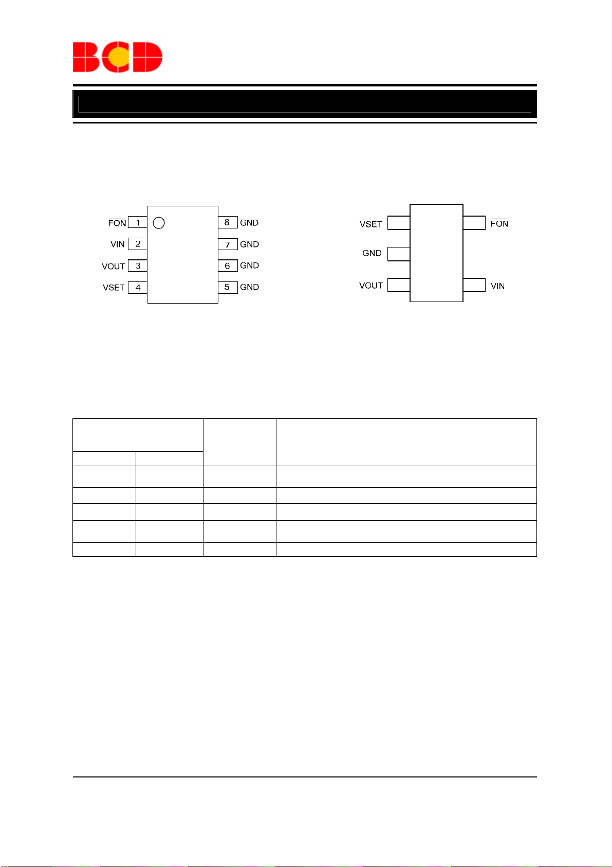
Pin Configuration
M Package K Package
(SOIC-8) (SOT-23-5)
Figure 2. Pin Configuration of AP2113 (Top View)
Pin Descriptions
Pin Number
SOIC-8 SOT-23-5
1 5
2 4 VIN Input voltage
3 3 VOUT Output voltage
4 1 VSET
5, 6, 7, 8 2 GND Ground
Pin Name Function
________
FON
Full speed mode / Adjustable mode selection input pin.
Set low for full speed mode, set high for adjustable mode with 1.6x
Voltage input pin, apply DC voltage into VSET as voltage
reference, the output voltage follows 1.6 times of
1
2
34
5
VSET voltage
Mar. 2012 Rev 1. 3 BCD Semiconductor Manufacturing Limited
2
Page 3
Preliminary Datasheet
1.6x Linear DC Fan Driver with VOUT Fully on Control AP2113
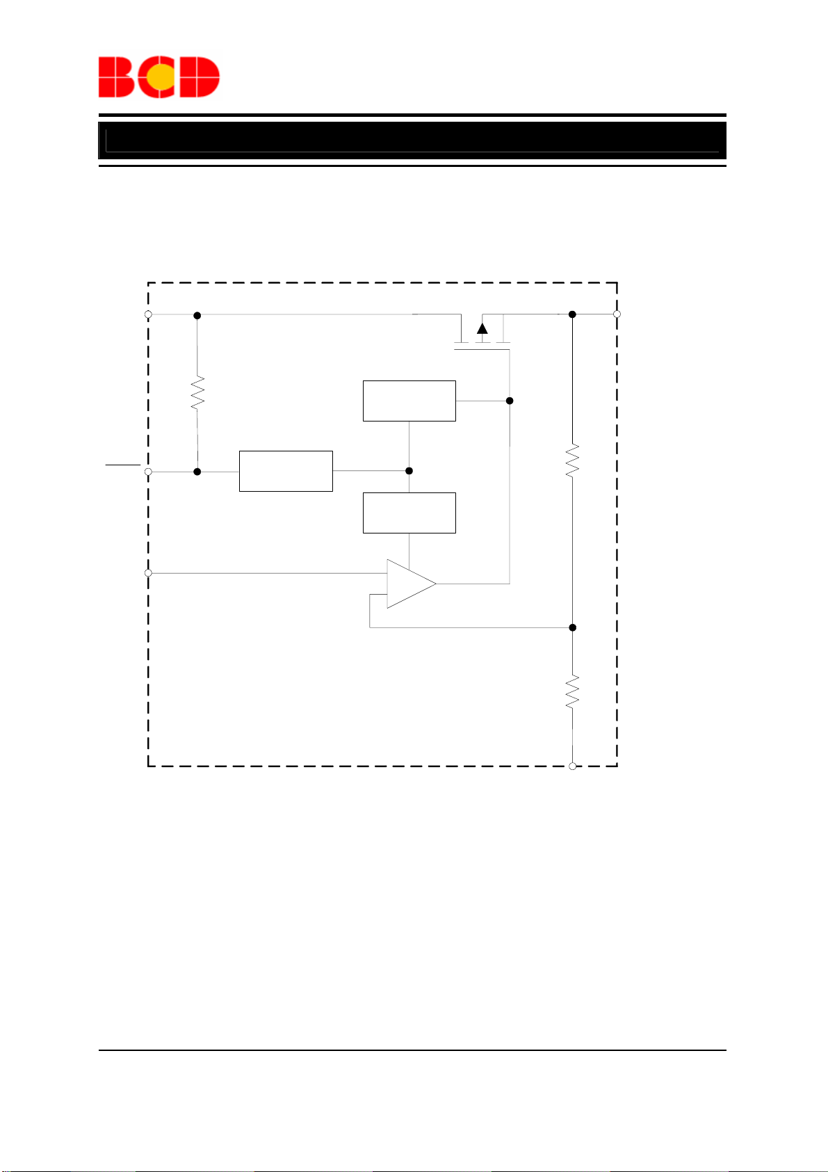
Functional Block Diagram
VIN
FON
VSET
2(4)
1(5)
4(1)
V
OUT
Fully on
Logic
Thermal
Shutdown
Short-Circuit
Protection
-
+
R1=0.6xR2
R1
R2
3(3)
VOUT
A(B)
5, 6, 7, 8 ( 2)
A for SOIC-8
B for SOT-23-5
GND
Figure 3. Functional Block Diagram of AP2113
Mar. 2012 Rev 1. 3 BCD Semiconductor Manufacturing Limited
3
Page 4
Preliminary Datasheet
1.6x Linear DC Fan Driver with VOUT Fully on Control AP2113
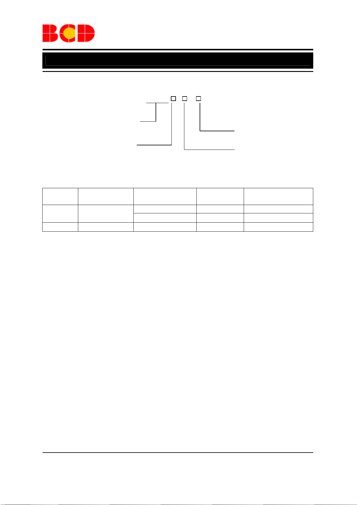
Ordering Information
AP2113 -
Circuit Type
Package
M: SOIC-8
K: SOT-23-5
Package
SOIC-8
SOT-23-5
BCD Semiconductor's Pb-free products, as designated with "G1" suffix in the part number, are RoHS compliant
and Green.
Temperature
Range
-40 to 85°C
-40 to 85°C
Part Number Marking ID Packing Type
AP2113M-G1 2113M-G1 Tube
AP2113MTR-G1 2113M-G1 Tape & Reel
AP2113KTR-G1 G5O Tape & Reel
G1: Green
Blank: Tube
TR: Tape & Reel
Mar. 2012 Rev 1. 3 BCD Semiconductor Manufacturing Limited
4
Page 5

Preliminary Datasheet
1.6x Linear DC Fan Driver with VOUT Fully on Control AP2113
Absolute Maximum Ratings (Note 1)
Parameter Symbol Value Unit
Input Voltage VIN 6.0 V
VSET Input Voltage V
________
FON
Input Voltage
Operating Junction Temperature
Range
Storage Temperature Range T
Thermal Resistance (Junction to
Ambient)(No Heat Sink)
ESD (Machine Model)
ESD (Human Body Model)
Note 1: Stresses greater than those listed under “Absolute Maximum Ratings” may cause permanent damage to
the device. These are stress ratings only, and functional operation of the device at these or any other conditions
beyond those indicated under “Recommended Operating Conditions” is not implied. Exposure to “Absolute
Maximum Ratings” for extended periods may affect device reliability.
5.5 V
SET
150 ºC
T
J
-65 to 150 ºC
STG
θ
JA
6000 V
SOIC-8 144 °C/W
5.5 V
300 V
Recommended Operating Conditions
Parameter Symbol Min Max Unit
Input Voltage VIN 2.5 5.5 V
Operating Ambient Temperature
Range
-40 85 °C
T
A
Mar. 2012 Rev 1. 3 BCD Semiconductor Manufacturing Limited
5
Page 6

_
_
_
Preliminary Datasheet
1.6x Linear DC Fan Driver with VOUT Fully on Control AP2113
Electrical Characteristics
VIN=5.0V, V
range, -40°C≤T
Parameter Symbol Conditions Min Typ Max Unit
=2V, CIN=1µF, C
SET
≤85°C ranges, unless otherwise specified.
A
=1µF, Typical TA=25°C, Bold typeface applies over full temperature
OUT
Quiescent Current IQ
Output Current I
Output Voltage/
VSET Voltage
Line Regulation
Load Regulation
V
(V△
(V△
OUT/VSET
OUT/VOUT
△VIN
OUT/VOUT
△I
Dropout Voltage V
Minimum VSET Voltage V
VSET Pin Current I
Fold-back Short Current I
SHORT
Output Current Limit I
_______
FON
Logic Input High
Level
_______
FON
Logic Input Low
Level
_______
FON
Pin Bias Current
Thermal Shutdown
Temperature
Thermal Shutdown
Hysteresis
T
T
HYOTSD
V
=5V, No Load
FON
V
=0V, No Load
FON
V
OUT
OUT
DROP
1 V
SET
V
SET
V
LIMIT
V
I
OUT
)
VIN=V
)
1mA ≤ I
VIN=5V, V
VIN=5V, V
=5.0V, V
IN
=5.5V, V
IN
OUT
=1V to 3.2V,
SET
=30mA
+1V to 5.5V, I
OUT
≤600mA 0.2 1 %/A
OUT
=2V,
SET
=2V,
SET
=5V 1
SET
=0V 50 mA
OUT
70 100
45
µA
µA
=3.2V 600 mA
1.552 1.6 1.648 V/V
=30mA 0.02 0.1 %/V
OUT
V
=0V , I
FON
V
=5V , I
FON
=600mA
OUT
=600mA
OUT
150 200 mV
200 250 mV
µA
1000 mA
1.6 5.5 V
0 0.4 V
=0V
1.5 10
µA
OTSD
V
FON
165
°C
25
Mar. 2012 Rev 1. 3 BCD Semiconductor Manufacturing Limited
6
Page 7

Preliminary Datasheet
1.6x Linear DC Fan Driver with VOUT Fully on Control AP2113
Typical Performance Characteristics
0.10
Supply Current (mA)
V
=5V
FON
=2V
V
SET
0.08
0.06
0.04
0.02
0.00
=0mA
I
OUT
TA=-40oC
TA=25oC
TA=85oC
Continuous Airflow 10scfm
0.0 0.5 1.0 1.5 2.0 2.5 3.0 3.5 4.0 4.5 5.0 5.5
Input Voltage (V)
Figure 4. Supply Current vs. Input Voltage Figure 5. Supply Current vs. Input Voltage
100
VIN=5V
95
I
=0A
OUT
90
Continuous Airflow 10scfm
85
80
75
70
65
Supply Current (µA)
60
55
50
45
-40 -20 0 20 40 60 80 100
Temperature (OC)
Full Speed Mode
Adjustable Mode
Figure 6. Supply Current vs. Temperature
Mar. 2012 Rev 1. 3 BCD Semiconductor Manufacturing Limited
7
0.10
V
=0V
FON
=0mA
I
OUT
0.08
0.06
0.04
Supply Current (mA)
0.02
0.00
Output Voltage (V)
TA=-40oC
TA=25oC
TA=85oC
Continuous Airflow 10scfm
0.0 0.5 1.0 1.5 2.0 2.5 3.0 3.5 4.0 4.5 5.0 5.5
Input Voltage (V)
5.0
VIN=5V
4.5
4.0
3.5
3.0
2.5
2.0
1.5
=10mA
I
OUT
TA=-40OC
TA=25OC
TA=85OC
Continuous Airflow 10scfm
1.0 1.5 2.0 2.5 3.0
V
Voltage (V)
SET
Figure 7. Output Voltage vs. V
SET
Voltage
Page 8

Preliminary Datasheet
1.6x Linear DC Fan Driver with VOUT Fully on Control AP2113
Typical Performance Characteristics (Continued)
6.0
5.5
5.0
4.5
4.0
3.5
3.0
2.5
2.0
Output Voltage (V)
1.5
1.0
0.5
0.0
0.0 0.2 0.4 0.6 0.8 1.0 1.2 1.4
Figure 8. Output Voltage vs. Output Current Figure 9. Dropout Voltage vs. Output Current
Continuous Airflow 10scfm
Output Current (A)
VIN=5V, V
C
IN=COUT
TC=25oC
V
V
V
V
FON
=1µF
SET
SET
SET
SET
=5V
=1.5V
=2.0V
=2.5V
=3.0V
1.8
I
1.6
1.4
1.2
1.0
0.8
0.6
0.4
FON Logic Low Level (V)
0.2
0.0
=0mA
OUT
TA=-40oC
TA=25oC
TA=85oC
Continuous Airflow 10scfm
123456
Input Voltage (V)
Figure 10. FON
________
Logic Low Level vs. Input Voltage Figure 11. FON
Mar. 2012 Rev 1. 3 BCD Semiconductor Manufacturing Limited
8
0.20
Full Speed Mode
0.18
0.16
0.14
0.12
0.10
0.08
0.06
Dropout Voltage (V)
0.04
0.02
0.00
1.8
1.6
1.4
1.2
1.0
0.8
0.6
0.4
FON Logic High Level (V)
0.2
0.0
TA=-40OC
TA=25OC
TA=85OC
Continuous Airflow 10scfm
0.0 0.1 0.2 0.3 0.4 0.5 0.6
Output Current (A)
Continuous Airflow 10scfm
I
=0mA
OUT
TA=-40oC
TA=25oC
TA=85oC
123456
Input Voltage (V)
________
Logic High Level vs. Input Voltage
Page 9

Preliminary Datasheet
1.6x Linear DC Fan Driver with VOUT Fully on Control AP2113
Typical Performance Characteristics (Continued)
(V
IN
Figure 12. Load Transient
=5V, V
=2V, CIN=C
SET
Slew Rate=250mA/µs)
V
FON
=5V,
=1µF,
OUT
Figure 13. Mode Change Delay Time (V
FON
Off)
Figure 14. Mode Change Delay Time (V
FON
On)
Mar. 2012 Rev 1. 3 BCD Semiconductor Manufacturing Limited
9
Page 10

Preliminary Datasheet
1.6x Linear DC Fan Driver with VOUT Fully on Control AP2113
Typical Application
Figure 15. Typical Application of AP2113
Mar. 2012 Rev 1. 3 BCD Semiconductor Manufacturing Limited
10
Page 11

Preliminary Datasheet
1.6x Linear DC Fan Driver with VOUT Fully on Control AP2113
Mechanical Dimensions
SOIC-8 Unit: mm(inch)
1.000(0.039)
4.700(0.185)
5.100(0.201)
7
°
7
°
1.270(0.050)
TYP
0.100(0.004)
0.300(0.012)
1.350(0.053)
1.750(0.069)
0.675(0.027)
0.725(0.029)
R0.150(0.006)
3.800(0.150)
4.000(0.157)
D
2
°
0
°
8
D
0
1
:
0.320(0.013)
5.800(0.228)
6.200(0.244)
0.800(0.031)
°
8
°
8
0.200(0.008)
0.330(0.013)
0.510(0.020)
0.190(0.007)
0.250(0.010)
0.900(0.035)
1°
5°
0.450(0.017)
0.800(0.031)
)
6
0
0
.
0
(
0
5
1
.
0
R
Note: Eject hole, oriented hole and mold mark is optional.
Mar. 2012 Rev 1. 3 BCD Semiconductor Manufacturing Limited
11
Page 12

Preliminary Datasheet
1.6x Linear DC Fan Driver with VOUT Fully on Control AP2113
Mechanical Dimensions (Continued)
SOT-23-5 Unit: mm(inch)
2.820(0.111)
0.100(0.004)
0.200(0.008)
0°
8°
0.950(0.037)
Y
T
P
3.020(0.119)
1.800(0.071)
2.000(0.079)
0.300(0.012)
0.400(0.016)
0.200(0.008)
0
.
0
0
(
7
0
.
E
F
R
0
)
8
2
0
0
.
0
1
.
0
9
0
.
0
0
(
0
(
0
0
3
.
1
Mar. 2012 Rev 1. 3 BCD Semiconductor Manufacturing Limited
12
0
0
.
0
0
0
(
)
0
0
.
0
0
5
(
)
6
0
3
0
.
5
)
.
)
1
5
0
Page 13

BCD Semiconductor Manufacturing Limited
IMPORTANT NOTICE
IMPORTANT NOTICE
BCD Semiconductor Manufacturing Limited reserves the right to make changes without further notice to any products or specifi-
BCD Semiconductor Manufacturing Limited reserves the right to make changes without further notice to any products or specifi-
cations herein. BCD Semiconductor Manufacturing Limited does not assume any responsibility for use of any its products for any
cations herein. BCD Semiconductor Manufacturing Limited does not assume any responsibility for use of any its products for any
particular purpose, nor does BCD Semiconductor Manufacturing Limited assume any liability arising out of the application or use
particular purpose, nor does BCD Semiconductor Manufacturing Limited assume any liability arising out of the application or use
of any its products or circuits. BCD Semiconductor Manufacturing Limited does not convey any license under its patent rights or
of any its products or circuits. BCD Semiconductor Manufacturing Limited does not convey any license under its patent rights or
other rights nor the rights of others.
other rights nor the rights of others.
http://www.bcdsemi.com
MAIN SITE
MAIN SITE
- Headquarters
BCD Semiconductor Manufacturing Limited
BCD Semiconductor Manufactur ing Limited
- Wafer Fab
No. 1600, Zi Xing Road, Shanghai ZiZhu Science-based Industrial Park, 200241, China
Shanghai SIM-BCD Semiconductor Manufacturing Limited
Tel: +86-21-24162266, Fax: +86-21-24162277
800, Yi Shan Road, Shanghai 200233, China
Tel: +86-21-6485 1491, Fax: +86-21-5450 0008
REGIONAL SALES OFFICE
Shenzhen Office
REGIONAL SALES OFFICE
Shanghai SIM-BCD Semiconductor Manufacturing Co., Ltd., Shenzhen Office
Shenzhen Office
Unit A Room 1203, Skyworth Bldg., Gaoxin Ave.1.S., Nanshan District, Shenzhen,
Shanghai SIM-BCD Semiconductor Manufacturing Co., Ltd. Shenzhen Office
China
Advanced Analog Circuits (Shanghai) Corporation Shenzhen Office
Tel: +86-755-8826 7951
Room E, 5F, Noble Center, No.1006, 3rd Fuzhong Road, Futian District, Shenzhen 518026, China
Fax: +86-755-8826 7865
Tel: +86-755-8826 7951
Fax: +86-755-8826 7865
- Wafer Fab
BCD Semiconductor Manufacturing Limited
Shanghai SIM-BCD Semiconductor Manufacturing Co., Ltd.
- IC Design Group
800 Yi Shan Road, Shanghai 200233, China
Advanced Analog Circuits (Shanghai) Corporation
Tel: +86-21-6485 1491, Fax: +86-21-5450 0008
8F, Zone B, 900, Yi Shan Road, Shanghai 200233, China
Tel: +86-21-6495 9539, Fax: +86-21-6485 9673
Taiwan Office
BCD Semiconductor (Taiwan) Company Limited
Taiwan Office
4F, 298-1, Rui Guang Road, Nei-Hu District, Taipei,
BCD Semiconductor (Taiwan) Company Limited
Tai wan
4F, 298-1, Rui Guang Road, Nei-Hu District, Taipei,
Tel: +886-2-2656 2808
Taiwan
Fax: +886-2-2656 2806
Tel: +886-2-2656 2808
Fax: +886-2-2656 2806
USA Office
BCD Semiconductor Corp.
USA Office
30920 Huntwood Ave. Hayward,
BCD Semiconductor Corporation
CA 94544, USA
30920 Huntwood Ave. Hayward,
Tel : +1-510-324-2988
CA 94544, U.S.A
Fax: +1-510-324-2788
Tel : +1-510-324-2988
Fax: +1-510-324-2788
 Loading...