

Page 1
AP2014/A
SYNCHRON O US PWM CONTROLL E R
Features
• Synchronous Controller in 8-Pin Package
• Operating with single 5V or 12V supply voltage
• Internal 200KHz Oscillator (400KHz for AP2014A)
• Soft-Start Function
• Fixed Frequency Voltage Mode
• 500mA Peak Output Drive Capability
• Protects the output when control FET is shorted
• Lead Free Package SOP-8L
• SOP-8L: Available in “Green” Molding Compound
(No Br, Sb)
• Lead Free Finish/ RoHS Compliant (Note 1)
Applications
• Graphic Card
• Hard Disk Drive
• DDR memory source sink Vtt application
• Low cost on-board DC to DC such as 5V to 3.3V, 2.5V or 1.8V
Ordering Information
AP 2014/A S X - 13
General Description
The AP2014 controller IC is designed to provide a low cost
synchronous Buck regulator for on-board DC to DC converter
applications. With today’s ASIC products requiring supply voltages
at 1.8V and lower, when the output current is as much as 3A and
the input voltage is at either 3.3V or 5V, traditional linear regulator
simply incurs too much loss within itself. The AP2014 together with
dual N-channel MOSFETs provide a low cost solution for such
applications. This device features an internal 200KHz oscillator
(400KHz for "A" version), under-voltage lockout for both Vcc and
Vc supplies, an external programmable soft-start function as well
as output under-voltage detection that latches off the device when
an output short is detected.
Package PackingLead Free
S : SOP-8L
L : Lead Free
G : Green
13 : Tape & Reel
Device
AP2014SL-13 S SOP-8L 2500/Tape & Reel -13
Lead-free
Package
Code
Packaging
(Note 2)
Quantity Part Number Suffix
AP2014SG-13 S SOP-8L 2500/Tape & Reel -13
AP2014ASL-13 S SOP-8L 2500/Tape & Reel -13
Lead-free
AP2014ASG-13 S SOP-8L 2500/Tape & Reel -13
Notes: 1. EU Directive 2002/95/EC (RoHS). All applicable RoHS exemptions applied, see EU Directive 2002/95/EC Annex Notes.
2. Pad layout as shown on Diodes Inc. suggested pad layout document AP02001, which can be found on our website at
http://www.diodes.com/datasheets/ap02001.pdf
.
13” Tape and Reel
AP2014/A Rev. 5 1 of 14 FEBRUARY 2009
www.diodes.com © Diodes Incorporated
Page 2
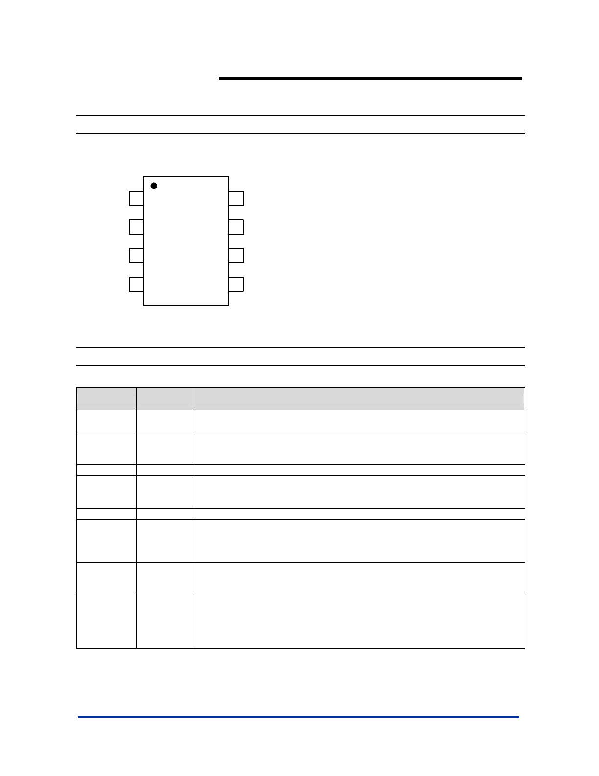
Pin Assignment
( Top View )
AP2014/A
SYNCHRON O US PWM CONTROLL E R
1
FB
VCC
LDrv
GND
2
3
4
SOP-8L
8
7
6
5
SS
Comp
Vc
HDrv
Pin Descriptions
Pin Name Pin No. Description
FB 1
Vcc 2
LDrv 3 Output driver for the s ynchronous power MOSFET.
GND 4
HDrv 5 Output driv er for the high side power MOS F ET.
Vc 6
Comp 7
SS 8
This pin is connected directly to the output of the switching regulator via resistor
divider to provide feedback to the Error amplifier.
This pin provides biasing for the internal blocks of the IC as well as power for the
low side driver. A minimum of 1uF, high frequency capacitor must be connected
from this pin to ground to provide peak drive current capability.
This pin serves as the ground pin and must be connected directly to the ground
plane. A high frequency capacitor (0.1 to 1u F) must be connecte d from V5 and
V12 pins to this pin for noise free operation.
This pin is connected to a voltage that must be at least 4V higher than the bus
voltage of the switcher (assuming 5V threshold MOSFET) and powers the high
side output driver. A minimum of 1uF, high frequency capacitor must be
connected from this pin to ground to provide peak drive current capability.
Compensation pin of the error amplifier. An external resistor and capacitor
network is typically connected from this pin to ground to provide loop
compensation.
This pin provides soft-start for the switching regulator. An internal current source
charges an external capacitor that is connected from this pin to ground which
ramps up the output of the switching regulator, preventing it from overshooting as
well as limi ting the inpu t current. T he converter c an be shutdown by pulling thi s
pin below 0.5V.
AP2014/A Rev. 5 2 of 14 FEBRUARY 2009
www.diodes.com © Diodes Incorporated
Page 3
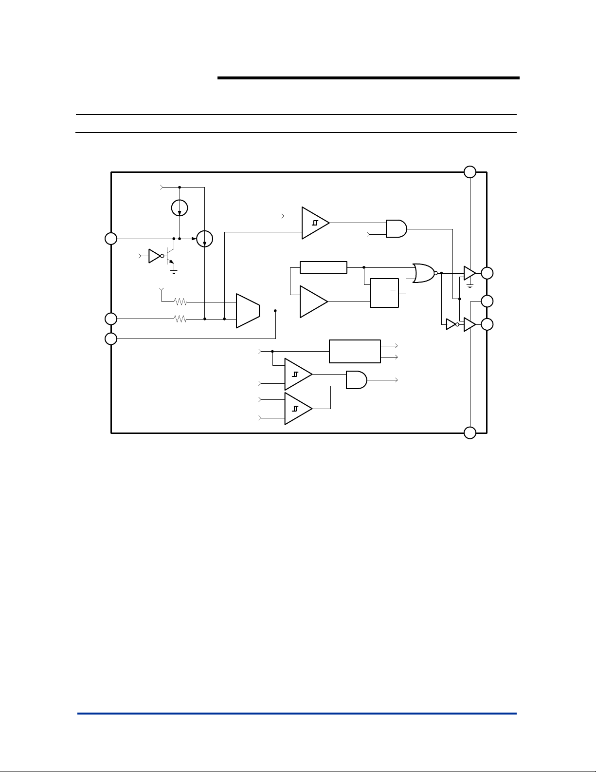
Block Diagram
3V
AP2014/A
SYNCHRON O US PWM CONTROLL E R
Vc
6
Comp
SS
Fb
Ct
0.2V
+
-
0.2V
+
-
FbLo Comp
-
+
Oscillator
Error Comp
+
-
POR
Bias
Generator
S
Q
R
Reset Dom
3V
1.25V
POR
4
GND
HDrv
5
2
Vcc
3
LDrv
20uA
8
POR
1.25V
1
7
64uA
Max
25K
25K
0.5V
Error Amp
+
-
Vcc
4.0V
Vc
3.5V
AP2014/A Rev. 5 3 of 14 FEBRUARY 2009
www.diodes.com © Diodes Incorporated
Page 4
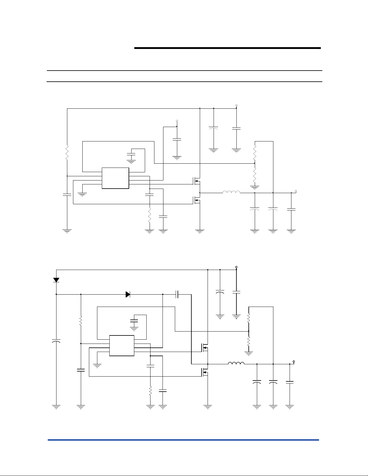
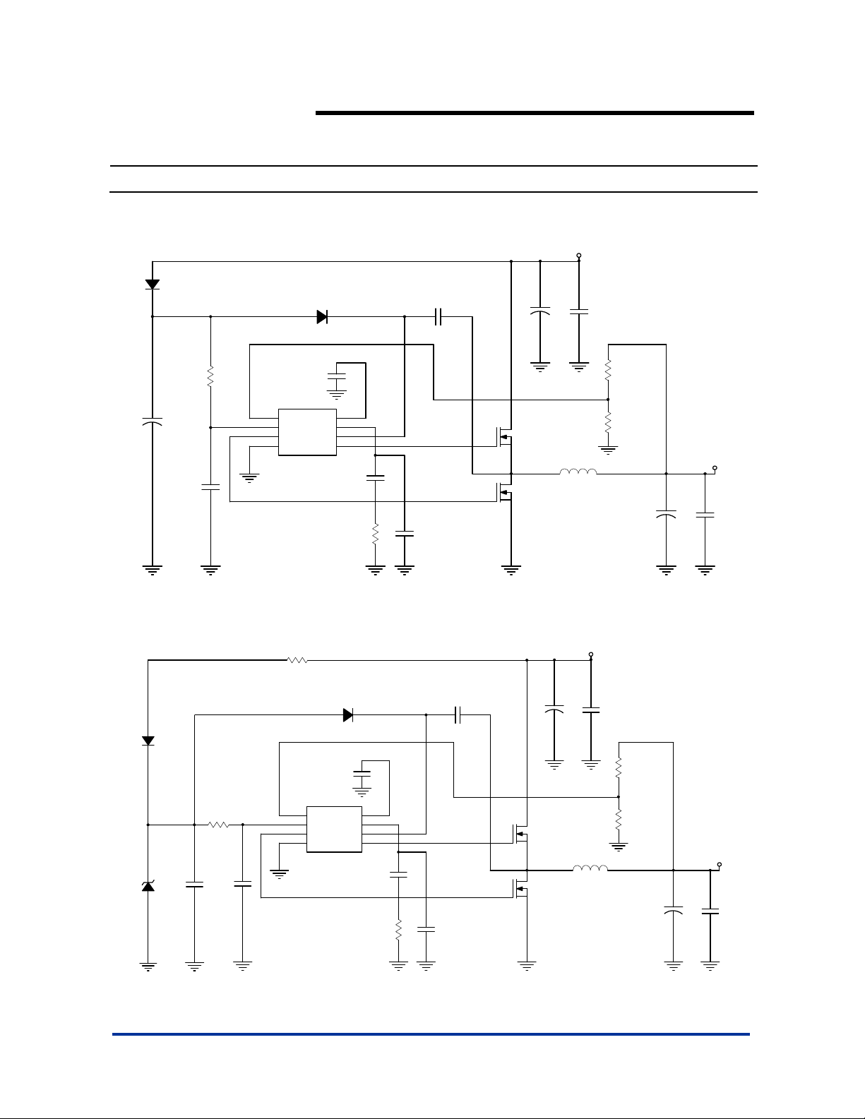
T ypical Application Circuit
(1)
R3
8.2
C5
0.47u
1
2
3
45
C4
0.1u
U1
FB
SS
Vcc
Comp
LDrv
GND HDrv
Vc
AP2014
8
7
6
C6
10nF
22k
R6
Vc=12V
C20
100p
AP2014/A
SYNCHRON O US PWM CONTROLL E R
VIN=5V
C3
1u
Q1
Q2
C8
470u
L1
5.6u/9.0
C11
0.1u
R1
820
R2
3.3K
C12
470u
Vout +1.5V/7.0A
C13
470u
C17
0.1u
(2)
D2
1N4148
C3
100u
C5
0.47u
R3
8.2
D1
1N4148
C4
0.1u
U1
1
FB
Vcc
LDrv
GND
SS
Comp
Vc
HDrv
2
3
4 5
AP2014
8
7
6
C6
10nF
R6
6.8k
C1
0.1uF
C20
100p
Option
Q1
Q2
C8
470u
L1
5.6u/9A
VIN=12V
C11
0.1u
R1
820
R2
3.3K
C12
470u
Vout +1.5V/7.0A
C13
C17
470u
0.1u
Single Supply 12V Input
AP2014/A Rev. 5 4 of 14 FEBRUARY 2009
www.diodes.com © Diodes Incorporated
Page 5
T ypical Application Circuit (Continued)
(3)
D2
1N4148
D1
1N4148
C1
0.1uF
AP2014/A
SYNCHRON O US PWM CONTROLL E R
VIN=12V
C8
C11
470u
0.1u
(4)
C3
100u
C5
0.47u
D2
1N4148
R3
8.2
R3
8.2
C4
0.1u
U1
1
FB
Vcc
LDrv
GND
RZD
1.2K
SS
Comp
Vc
HDrv
1N4148
C4
0.1u
2
3
4 5
AP2014
8
7
6
C6
10nF
R6
39k
C20
100p
Single Supply 12V Input
D1
C1
0.1uF
Q1
Q2
L1
10uH/6A
C8
470u
R1
10K
R2
3K
VIN=24V
C11
0.1u
R1
10K
Vout +5V/5.0A
C13
470u
C17
0.1u
U1
ZD
6.2V
C3
100u
R3
8.2
C5
0.47u
1
FB
2
Vcc
3
LDrv
4 5
GND
AP2014
SS
Comp
Vc
HDrv
8
7
6
C6
10nF
R6
47k
C20
100p
Q1-1
Q1-2
L1
10uH/6A
R2
3.3K
Vout +5V/4.0A
C13
C17
0.1u
470u
IZD(≧15mA)=(VIN-VD2-VZD)/RZD
Single Supply 24V Input
AP2014/A Rev. 5 5 of 14 FEBRUARY 2009
www.diodes.com © Diodes Incorporated
Page 6

T ypical Application Circuit (Continued)
(5)
+12V
AP2014/A
SYNCHRON O US PWM CONTROLL E R
+12V
R7
0R
C11
0.1u
R4
0R
Q1
70T03H
Q2
70T03H
C7
470u
D2
SBD
optional
C3
1u
C4
0.1u
U1
1
FB
2
Vcc
3
R3
11
C5
1u
LDrv
45
GND HDrv
AP2014A
SS
Comp
Vc
C6
5600pF
8
7
6
R6
39k
R9
R
C20
10p
C9
470u
L1
4.7u
+12V_BUS
C10
470u
R1
2.2K
R2
1K
C12
470u
C13
470u
Vout +1.26V
C15
470u
C17
0.1u
AP2014/A Rev. 5 6 of 14 FEBRUARY 2009
www.diodes.com © Diodes Incorporated
Page 7

T ypical Application Circuit (Continued)
(6) Dual Supply, 5V Bus and 12V Bias Input
5V
12V
C1
0.1uF
C1
1uF
AP2014/A
SYNCHRON O US PWM CONTROLL E R
L1
+
C3
100uF
1uH
+
C4
47uF
+
C5
1.8V/1A
47uF
2.5V/2A
3.3V/1.8A
10nF
3.3K
C14
10nF
R4
3.3K
C8
R1
0.1uF
C9
0.1uF
C13
0.1uF
Comp
C7
Comp
Vcc
AP2014
SS
Vcc
SS
Vc
HDrv
GND
Vc
HDrv
AP2014
GND
LDrv
Fb
LDrv
Fb
1K
R5
1K
R2
C10
1uF
Q1
Q2
Q3
Q4
R3
1K
+
C11
R6
1.65K
L2
10uH
L3
10uH
AP1187
+
C6
220uF
+
C12
220uF
Dual Supply, 5V Bus and 12V Bias Input
AP2014/A Rev. 5 7 of 14 FEBRUARY 2009
www.diodes.com © Diodes Incorporated
Page 8

AP2014/A
SYNCHRON O US PWM CONTROLL E R
Absolute Maximum Ratings
Symbol Parameter Rating Unit
VCC VCC Supply Voltage 20 V
Vc Vc Supply Voltage (not rated for inductive load) 32 V
T
Storage Temperature Range -65 to +150
ST
TOP Operating Junction Temperature Range 0 to +125
θ
Thermal Resistance Junction to Case 7
JC
θ
Thermal Resistance Junction to Ambient 160
JA
Notes: 3. Test condit ions for SOP-8L: Device mounted on 2oz copper, minimum recommended pad layout, FR-4 PCB.
o
o
o
C/W
o
C/W
Electrical Characteristics
Unless otherwise specified, these specifications apply over VCC=5V, VC=12V and TA=0 to 70°C. Typical values refer to TA =25°C. Low
duty cycle pulse testing is used which keeps junction and case temperatures equal to the ambient temperature.
Symbol Parameter Conditions Min. Typ. Max. Unit
Reference Voltage
VFB FB Voltage
L
FB Voltage Line Regulation 5 < Vcc < 12 - 0.2 0.35 %
REG
UVLO
UVLO VCC
UVLO VC
UVLO FB
UVLO Threshold - V
UVLO Hysteresis - VCC - 0.25 - V
UVLO Threshold - V
UVLO Hysteresis - VC - 0.2 - V
UVLO Threshold - FB
CC
C
UVLO Hysteresis - FB - 0.1 - V
Supply Current
Operation ICC VCC Operation Supply Current
Operation IC VC Operation Supply Current
I
VCC Static Supply Current SS=0V - 3.3 6 mA
CCQ
ICQ V
Static Supply Current SS=0V - 1 4.5 mA
C
Soft-Start Section
SSIB Charge Current SS=0V 10 20 30 μA
Error Amp
I
FB Voltage Input Bias Current SS=3V, FB=1V - -0.1 - μA
FB1
I
FB Voltage Input Bias Current SS=0V, FB=1V - -64 - μA
FB2
gm Transconductance 450 600 750 μmho
Oscillator
Freq Frequency
V
Ramp-Amplitude Voltage 1.225 1.25 1.275 V
RAMP
Output Drivers
Tr Rise Time CL =1500pF - 50 100 ns
Tf Fall Time CL =1500pF - 50 100 ns
TDB Dead Band Time 50 150 250 ns
TON Max Duty Cycle FB=1V, Freq=200KHz 85 90 95 %
T
Min Duty Cycle FB=1.5V 0 0 - %
OFF
AP2014 1.225 1.25 1.275
AP2014A 0.784 0.800 0.816
Supply Ramping Up
Supply Ramping Up
FB Ramping Down
(AP2014)
FB Ramping Down
(AP2014A)
Freq=200KHz,
C
=1500pF
L
Freq=200KHz,
C
=1500pF
L
4.0 4.2 4.4 V
3.1 3.3 3.5 V
0.4 0.6 0.8 V
0.3 0.4 0.5 V
- 7 10 mA
- 7 10 mA
V
AP2014 170 200 230 KHz
AP2014A 340 400 460 KHz
C
C
AP2014/A Rev. 5 8 of 14 FEBRUARY 2009
www.diodes.com © Diodes Incorporated
Page 9

Typical Performance Characteristics
AP2014/A
SYNCHRON O US PWM CONTROLL E R
2.0%
Load Regulation
1.8%
1.6%
1.4%
1.2%
1.0%
0.8%
0.6%
Load Regulation (%)
0.4%
0.2%
0.0%
0.0 0.5 1.0 3.0 5.0 8.0 10.0 12.0 15.0
Iout(A)
100%
90%
80%
70%
60%
50%
40%
30%
Efficiency (%)
20%
10%
0%
Efficiency vs. Iout
0.0 0.5 1.0 3.0 5.0 8.0 10.0 12.0 15.0
Iout(A)
1.260
1.255
1.250
1.245
Feedback Voltage (V)
1.240
Line Regulation
4.5 5.0 7.0 9.0 11.0 12.0 15.0
Vin(V)
2.530
2.525
2.520
2.515
2.510
2.505
Output Voltage (V)
2.500
Line Regulation
4.5 5.0 7.0 9.0 11.0 12.0 15.0
Vin(V)
Frequency (KHz)
210.0
205.0
200.0
195.0
190.0
185.0
180.0
175.0
Frequency vs. Vin
4.5 5.0 7.0 9.0 11.0 12.0 15.0
Vin(V)
240.0
230.0
220.0
210.0
200.0
190.0
180.0
Frequency (KHz)
170.0
160.0
150.0
Frequency vs. Temperature
-40 -20 0 25 50 75 100 125
Temperature (oC)
AP2014/A Rev. 5 9 of 14 FEBRUARY 2009
www.diodes.com © Diodes Incorporated
Page 10

SYNCHRON O US PWM CONTROLL E R
Typical Performance Characteristics (Continued)
AP2014/A
Icc and Iccq (mA)
15.00
13.00
11.00
9.00
7.00
5.00
3.00
Icc and Iccq vs. Vin
Icc(mA)
Iccq(mA)
4.5 5 7 9 11 12 15
Vin(V)
16.00
14.00
12.00
10.00
8.00
6.00
Ic and Icq (mA)
4.00
2.00
Ic and Icq vs. Vin
Ic(mA)
Icq(mA)
4.5 5 7 9 11 12 15
Vin(V)
10.0
9.5
9.0
8.5
8.0
7.5
7.0
Icc and Ic (mA)
6.5
6.0
Icc and Ic vs. Temperature
Icc(mA)
Ic(mA)
-40-200 255075100125
Temperature (oC)
1.30
1.28
1.26
1.24
1.22
Feedback Voltage (V)
1.20
Vfb vs. Temperature
-40 -20 0 25 50 75 100 125
Temperature (oC)
AP2014A Ic and Icc vs Vc
21.0
19.0
17.0
15.0
13.0
11.0
9.0
7.0
5.0
3.0
Ic(mA)
Icc(mA)
6 8 10 12 14 16 18 20 22 24
20.0
18.0
16.0
14.0
12.0
10.0
8.0
6.0
4.0
2.0
Vc(V)
AP2014 Ic and Icc vs Vc
Ic(mA)
Icc(mA)
6 8 10 12 14 16 18 20 22 24
Vc(V)
AP2014/A Rev. 5 10 of 14 FEBRUARY 2009
www.diodes.com © Diodes Incorporated
Page 11

V
V
SYNCHRON O US PWM CONTROLL E R
Typical Performance Characteristics (Continued)
out Ripple
Vcc=5V; Vc=12V; Vout=2.5V
Iout=0.5A, Vripple=30.8mV
Vcc=5V; Vc=12V; Vout=2.5V
Iout=5A, Vripple=33.2mV
AP2014/A
out Ripple
Vcc=5V, Vc=12V, Vout=2.5V, Iout=0.5A, Temp=28
Dead time = 150ns
Phase
Highside GATE
Lowside GATE
Vcc=5V, Vc=12V, Vout=2.5V, Iout=5A , Temp=28
Dead time = 160ns
Phase
Highside GATE
Dead time vs. Iout
Dead time vs. Iout
o
C
Dead time = 150ns
o
C
Dead time = 150ns
Lowside GATE
AP2014/A Rev. 5 11 of 14 FEBRUARY 2009
www.diodes.com © Diodes Incorporated
Page 12

AP2014/A
SYNCHRON O US PWM CONTROLL E R
Functional Descriptions
Introduction
The AP2014 is a fixed frequency, voltage mode synchronous controller and consists of a precision reference voltage, an error amplifier,
an internal oscillator, a PWM comparator, 0.5A peak gate driver, soft-start and shutdown circuits (see Block Diagram).
The output voltage of the synchronous converter is set and controlled by the output of the error amplifier; this is the amplified error signal
from the sensed output voltage and the reference voltage.
This voltage is compared to a fixed frequency linear sawtooth ramp and generates fixed frequency pulses of variable duty-cycle, which
drives the two N-channel external MOSFETs.The timing of the IC is provided through an internal oscillator circuit which uses on-chip
capacitor to set the oscillation frequency to 200 KHz (400 KHz for “A” version).
Soft-Start
The AP2014 has a programmable soft-start to control the output voltage rise and limit the current surge at the start-up. To ensure correct
start-up, the soft-start sequence initiates when the V
Power On Reset (POR) signal. Soft-start function operates by sourcing an internal current to charge an external capacitor to about 3V.
Initially, the soft-start function clamps the E/A’s output of the PWM converter. As the charging voltage of the external capacitor ramps up,
the PWM signals increase from zero to the point the feedback loop takes control.
Short-Circuit Prote ction
The outputs are protected against the short circuit. The AP2014 protects the circuit for shorted output by sensing the output voltage
(through the external resistor divider). The AP2014 shuts down the PWM signals, when the output voltage drops below 0.6V (0.4V for
AP2014A).
The AP2014 also pr ote cts the output from over- voltag ing when the co ntrol FET is s horted. This is d one b y turni ng o n the s ync FE T wi th
the maximum duty cycle.
Under-Voltage Lockout
The under-voltage lockout circuit assures that the MOSFET driver outputs remain in the off state whenever the supply voltage drops
below set parameters. Lockout occurs if V
rise above the set values.
IC Quiescent Power Dissipation
Power dissipation for IC controller is a function of applied voltage, gate driver loads and switching frequency. The IC's maximum power
dissipation occurs when the IC operating with single 12V supply voltage (Vcc=12V and Vc
maximum gate loads.
Page 8 shows voltage vs. current, when the gate drivers loaded with 1500pF capacitors. The IC's power dissipation results in an
excessive temperature rise. This should be considered when using AP2014A for such application.
and VCC fall below 3.3V and 4.2V respectively. Normal operation resumes once VC and VCC
C
and VCC rise above their threshold (3.3V and 4.2V respectively) and generates the
C
≅24V) at 400KHz switching frequency and
AP2014/A Rev. 5 12 of 14 FEBRUARY 2009
www.diodes.com © Diodes Incorporated
Page 13

Marking Information
(1) SOP-8L
AP2014/A
SYNCHRON O US PWM CONTROLL E R
( Top View )
8
5
Logo
Part Number
AP2014 : 200KHz (OSC)
AP2014X
WW X
YY
X
AP2014A : 400KHz (OSC)
41
Package Information (All Dimensions in mm)
(1) Package Type: SOP-8L
0.254
0.62/0.82
7°~9°
Gauge Plane
Seating Plane
Detail "A"
7°~9°
1.27typ
4.85/4.95
0.3/0.5
3.85/3.95
1.30/1.50
5.90/6.10
1.75max.
0.15/0.25
0.10/0.20
0.35max.
Detail "A"
45°
L : Lead Free
G : Green
: Year : 08, 09,10~
YY
WW : Week : 01~52; 52
represents 52 and 53 week
X
: Internal Code
0°/8°
8x-0.60
5.4
6x-1.27
8x-1.55
Land Pattern Recommendation
(Unit: mm)
AP2014/A Rev. 5 13 of 14 FEBRUARY 2009
www.diodes.com © Diodes Incorporated
Page 14

AP2014/A
SYNCHRON O US PWM CONTROLL E R
IMPORTANT NOTICE
Diodes Incorporated and its subsidiaries reserve the right to make modifications, enhancements, improvements, corrections or other changes without further
notice to any product herein. Diodes Incorporated does not assume any liability arising out of the application or use of any product described herein; neither
does it convey any license under its patent rights, nor the rights of others. The user of products in such applications shall assume all risks of such use and will
agree to hold Diodes Incorporated and all the companies whose products are represented on our website, harmless against all damages.
LIFE SUPPORT
Diodes Incorporated products are not authorized for use as critical components in life support devices or systems without the expressed written approval of the
President of Diodes Incorporated.
AP2014/A Rev. 5 14 of 14 FEBRUARY 2009
www.diodes.com © Diodes Incorporated
 Loading...