

Page 1
AP1690
Document number: DS36469 Rev. 2 - 2
1 of 9
www.diodes.com
May 2014
© Diodes Incorporated
AP1690
A Product Line of
Diodes Incorporated
NE W P R OD U C T
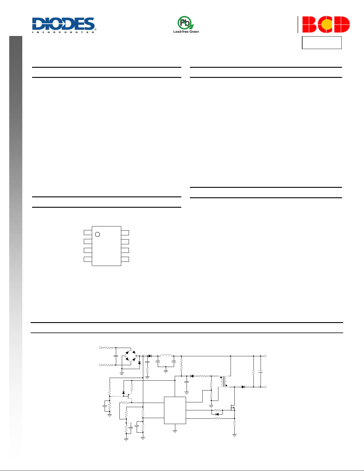
Description
The AP1690 is a high performance AC/DC universal input Primary
Side Regulation Power Factor Controller for dimmable LED driver
applications.
The AP1690 provides accurate constant current (CC) regulation while
removing the opto-coupler and secondary control circuitry. It also
eliminates the need of loop compensation circuitry while maintaining
stability. The AP1690 achieves excellent regulation and high
efficiency, yet meets the requirement of IEC61000-3-2 harmonic
standard.
The AP1690 features low start-up current, low operation current and
high efficiency. It also has rich protection features including over
voltage, short circuit, over current, over temperature protection etc. In
order to regulate the output current of LED current with the phase of
dimmer, pin 2 and pin 3 are used to set the peak current of
transformer according to the voltage applied to these two pins.
The AP1690 is available in SO-8 package.
Pin Assignments
(Top View)
(SO-8/ M Package)
Features
Primary Side Control for Output Current Regulation Without Opto-
coupler and Secondary CV/CC Control Circuitry
Low Start-up Current
Good Dimmer Compatibility
Tight CC Regulation Performance for Universal Input Mains
Voltage Range
Eliminates Control Loop Compensation Circuitry
Built-in Acceleration Start
LED Open Protection
LED Short Circuit Protection
Over Temperature Protection
Over Current Protection
Cost Effective for Dimmable LED Driver Solution
Totally Lead-Free & Fully RoHS Compliant (Notes 1 & 2)
Halogen and Antimony Free. “Green” Device (Note 3)
Applications
Single Stage Power Factor Correction Power Supply for
Dimmable LED Lighting
VCC
DIM
PD
GND
CS
OUT
FB
LED+
LED-
L
N
R1
R2
C1
BD1
ZD1
D1
C2
C3 C4
L1
R4
R5
R3
D2
R6
C5
R7
R8
C6
R9
R10
D3
R11
R12
R13
R14
C7
R
15
R16
C8
R17
R18
D4
Q1
R19
D5
R20
C9
+
Q2
AP1690
3
2
6
4
7
5
8
1
2
3
4
8
7
6
5
NC
PD
DIM
CS
FB
GND
OUT
VCC
SINGLE STAGE PRIMARY SIDE REGULATION PFC CONTROLLER FOR DIMMABLE LED DRIVER
Notes: 1. No purposely added lead. Fully EU Directive 2002/95/EC (RoHS) & 2011/65/EU (RoHS 2) compliant.
2. See http://www.diodes.com/quality/lead_free.html for more information about Diodes Incorporated’s definitions of Halogen- and Antimony-free, "Green"
and Lead-free.
3. Halogen- and Antimony-free "Green” products are defined as those which contain <900ppm bromine, <900ppm chlorine (<1500ppm total Br + Cl) and
<1000ppm antimony compounds.
Typical Applications Circuit
Non-isolated
Page 2
AP1690
Document number: DS36469 Rev. 2 - 2
2 of 9
www.diodes.com
May 2014
© Diodes Incorporated
AP1690
A Product Line of
Diodes Incorporated
NE W P R OD U C T
VCC
DIM
PD
GND
CS
OUT
FB
L
N
LED+
LED-
R1
C1
AP1690
ZD1
BD1
D1
L1
R2
C2
R3
C3
C4
R4
R5
R6
C5
D2
D3
R7
C6
R8
R9
R10
R11
C7
R12
R13
R14
R15
R16
R17
C8
C9
D4
D5
R18
R
19
R20
Q1
D6
C10
R21
CY1
T1
Q2
+
3
2
6
4
7
5
8
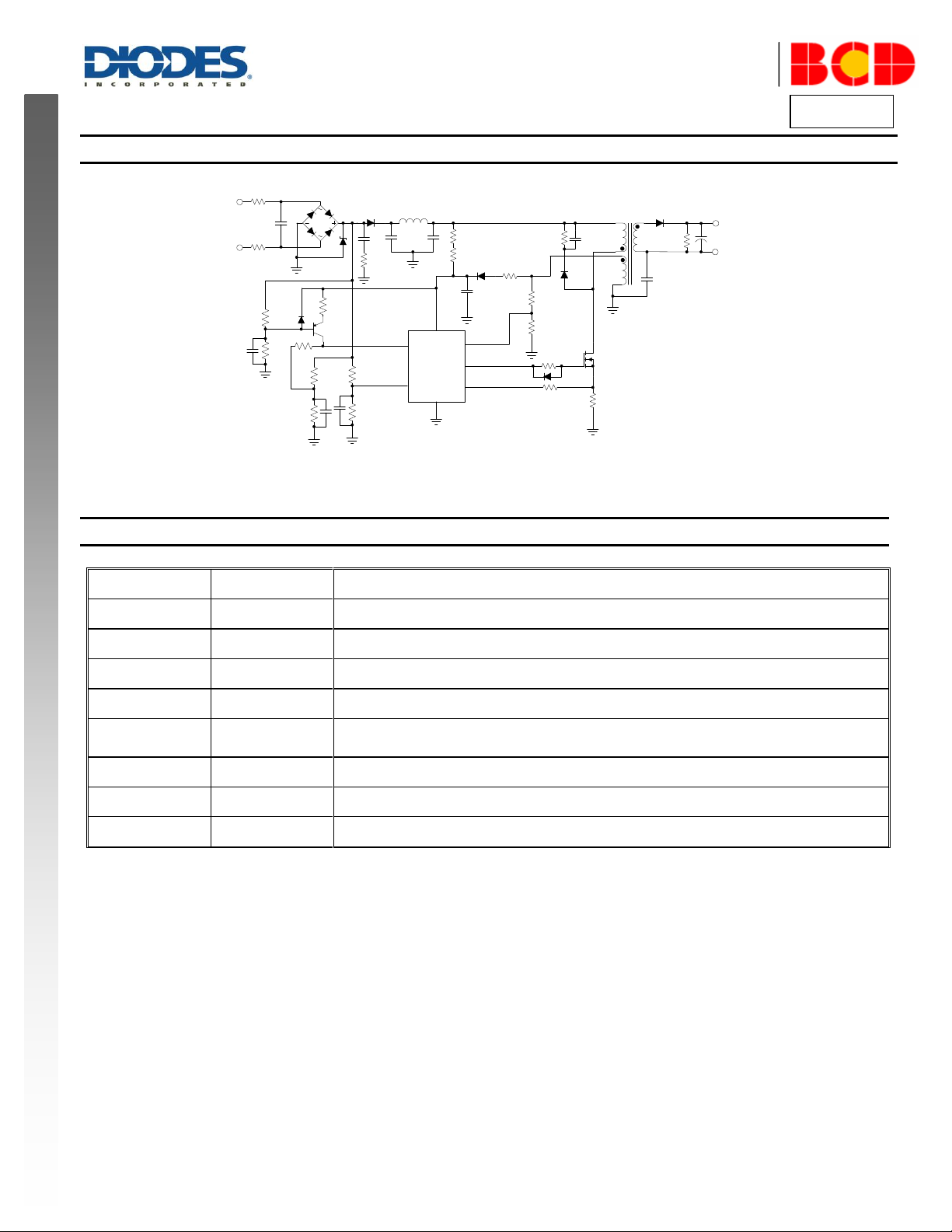
Pin Number
Pin Name
Function
1
NC
No connection
2
PD
The rectified input voltage sensing pin. The pin is detecting the phase of dimmer
3
DIM
The rectified input voltage sensing pin. The pin is detecting the average AC input voltage
4
CS
Primary current sensing
5
FB
This pin captures the feedback voltage from the auxiliary winding. FB voltage is used to control no
load output voltage and determine acceleration stop point at start-up phase
6
GND
Ground. Current return for gate driver and control circuits of the IC
7
OUT
Gate driver output
8
VCC
Supply voltage of gate driver and control circuits of the IC
Typical Applications Circuit (Cont.)
Isolated
Pin Descriptions
Page 3
AP1690
Document number: DS36469 Rev. 2 - 2
3 of 9
www.diodes.com
May 2014
© Diodes Incorporated
AP1690
A Product Line of
Diodes Incorporated
NE W P R OD U C T
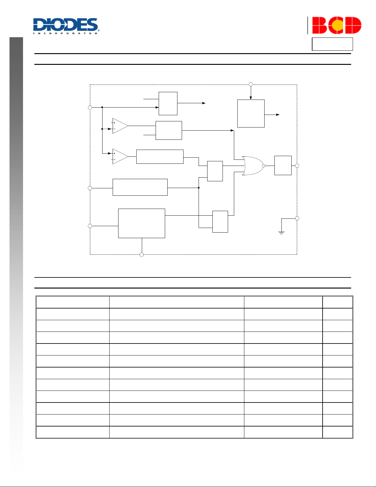
Regulator
&
Bias
OVP
Tonsec
Detector
0.1V
1.8V
PFM
Tons
UVLO
COMP
EA
UVLO
pro
CV_CTRL
PFM
Driver
R Q
S
R
Q
S
CC_CTRL
FB
CS
PD
VCC
OUT
GND
Acceleration Start
Control
Peak Current Control
& LEB
Dimming Control
DIM
2
3
4
5
6
7
8
Symbol
Parameter
Rating
Unit
VCC
Power Supply Voltage
-0.3 to 30
V
I
OUT
Driver Output Current
300
mA
VPD, V
DIM
, VCS
Voltage at PD, DIM, CS
-0.3 to 7
V
VFB
FB Input Voltage
-40 to 10
V
TJ
Operating Junction Temperature
+150
ºC
T
STG
Storage Temperature
-65 to +150
ºC
T
LEAD
Lead Temperature (Soldering, 10 sec)
+300
ºC
PD
Power Dissipation at TA = +50C
0.65
W
θ
JA
Thermal Resistance (Junction to Ambient)
190
C/W
–
ESD (Machine Model)
200
V
–
ESD (Human Body Model)
3000
V
Functional Block Diagram
Absolute Maximum Ratings (Note 4)
Note 4: Stresses greater than those listed under “Absolute Maximum Ratings” may cause permanent damage to the device. These are str ess ratings only, and
functional operation of the device at these or any other conditions beyond those indicated under “Recommended Operating Conditions” is not implied.
Exposure to “Absolute Maximum Ratings” for extended periods may affect device reliability.
Page 4
AP1690
Document number: DS36469 Rev. 2 - 2
4 of 9
www.diodes.com
May 2014
© Diodes Incorporated
AP1690
A Product Line of
Diodes Incorporated
NE W P R OD U C T
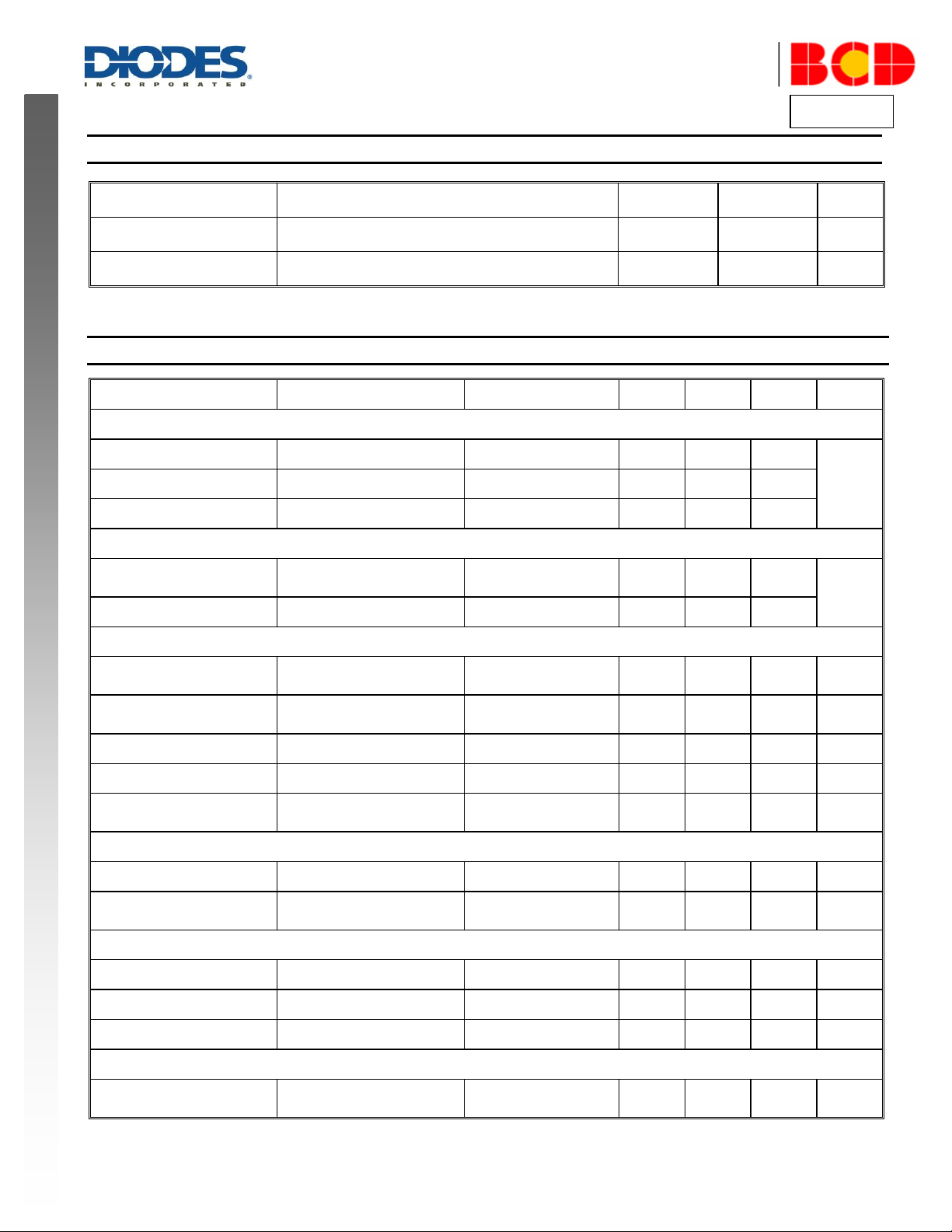
Symbol
Parameter
Min
Max
Unit
VCC
Power Supply Voltage
9
21
V
TA
Ambient Temperature
-40
+105
ºC
Symbol
Parameter
Conditions
Min
Typ
Max
Unit
UVLO Section
VTH (ST)
Start-up Threshold
–
18
19
20
V
V
OPR
(Min)
Minimal Operating Voltage
After turn on
7 8 9
V
CC_OVP
VCC OVP Voltage
–
28
32
36
Standby Current Section
IST
Start-up Current
V
CC
= VTH (ST)-0.5V,
Before start up
– – 100
µA
ICC (Max)
Maximum Operating Current
V
PD
= V
DIM
= 3V
–
1500
2000
Drive Output Section
VOH
Output High Level Voltage
I
GD-SOURCE
= 20mA
V
CC
= 12V
10 – –
V
VOL
Output Low Level Voltage
I
GD-SINK
= 20mA
V
CC
= 12V
– – 1
V
tR
Output Voltage Rise Time
CL = 1nF
100
140
190
ns
tF
Output Voltage Fall Time
CL = 1nF
30
60
90
ns
V
O-CLAMP
Output Clamp Voltage
I
GD-SOURCE
= 5mA
V
CC
= 20V
12
13.5
15
V
Current Sense Section
tON (Min)
Minimum On Time
–
500
750
1000
ns
V
SOCP
Short Circuit Protection
Voltage
– 3 4 – V
Feedback Input Section
IFB
FB Pin Input Leakage Current
V
FB
= 4V
– 2 8
µA
V
FB
(ACC)
Acceleration Start Threshold
–
1.4
1.8
2.2
V
V
FB
(OVP)
Over Voltage Protection
–
4.5 6 7.5
V
Dimming Section
VIN
PD Pin and DIM Pin Input
Voltage Range
– – 3 6 V
Recommended Operating Conditions
Electrical Characteristics (@V
= 15V, TA = +25°C, unless otherwise specified.)
CC
Page 5
AP1690
Document number: DS36469 Rev. 2 - 2
5 of 9
www.diodes.com
May 2014
© Diodes Incorporated
AP1690
A Product Line of
Diodes Incorporated
NE W P R OD U C T
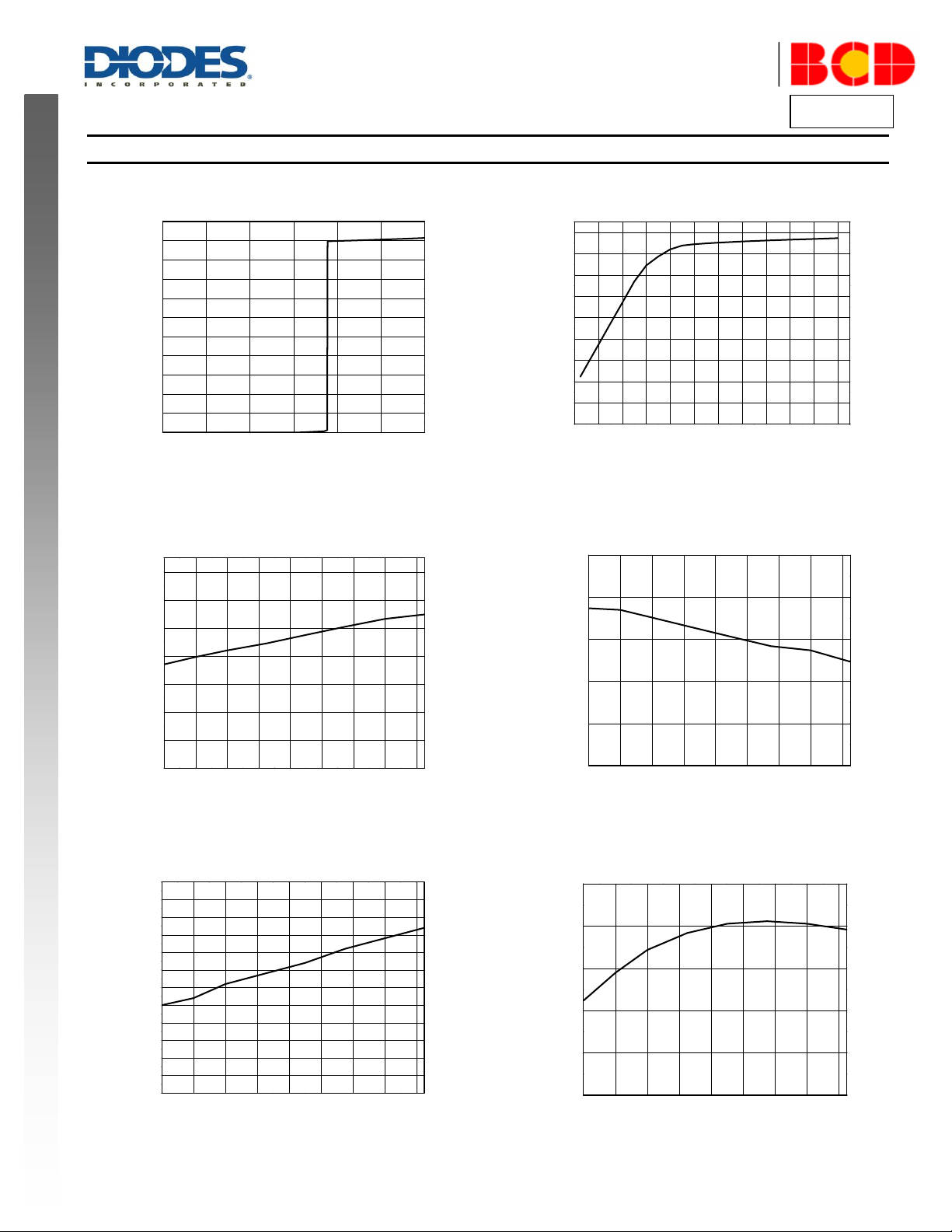
0 5 10 15 20 25 30
0
100
200
300
400
500
600
700
800
900
1000
1100
Supply Current (
A)
Supply Voltage (V)
8 10 12 14 16 18 20 22 24 26 28 30
5
6
7
8
9
10
11
12
13
14
Output Clamp Voltage (V)
Supply Voltage (V)
-40 -20 0 20 40 60 80 100 120
18.0
18.2
18.4
18.6
18.8
19.0
19.2
19.4
Start-up Voltage (V)
Ambient Temperature (oC)
-40 -20 0 20 40 60 80 100 120
7.8
7.9
8.0
8.1
8.2
8.3
Minimal Operating Voltage (V)
Ambient Temperature (oC)
-40 -20 0 20 40 60 80 100 120
2.0
2.5
3.0
3.5
4.0
4.5
5.0
5.5
6.0
6.5
7.0
7.5
8.0
Start-up Current (
A)
Ambient Temperature (oC)
-40 -20 0 20 40 60 80 100 120
800
850
900
950
1000
1050
Operating Current (
A)
Ambient Temperature (oC)
Performance Characteristics
Supply Current vs. Supply Voltage Output Clamp Voltage vs. Supply Voltage
Start-up Voltage vs. Ambient Temperature Minimal Operating Voltage vs. Ambient Temperature
Start-up Current vs. Ambient Temperature Operating Current vs. Ambient Temperature
Page 6
AP1690
Document number: DS36469 Rev. 2 - 2
6 of 9
www.diodes.com
May 2014
© Diodes Incorporated
AP1690
A Product Line of
Diodes Incorporated
NE W P R OD U C T
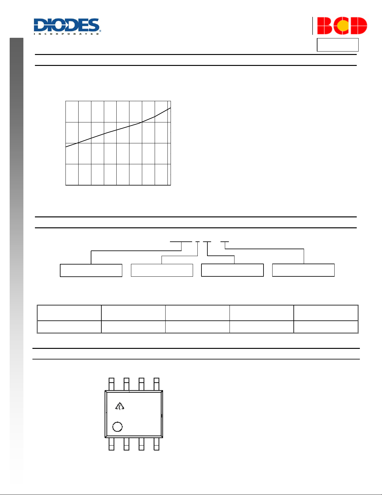
AP1690 X XX – G1
PackingPackageProduct Name
TR : Tape & Reel
M : SO-8
G1 : Green
RoHS/Green
Package
Temperature
Range
Part Number
Marking ID
Packing
SO-8
-40 to +105C
AP1690MTR-G1
1690M-G1
4000/13’’Tape & Reel
-40 -20 0 20 40 60 80 100 120
1.0
1.5
2.0
2.5
3.0
FB Input Leakage Current (
A)
Ambient Temperature (oC)
1690
M-G1
YWWAXX
First and Second Lines: Logo and Marking ID
(See Ordering Information)
Third Line: Date Code
Y: Year
WW: Work Week of Molding
A: Assembly House Code
XX: 7th and 8th Digits of Batch No.
Performance Characteristics (Cont.)
FB Input Leakage Current vs. Ambient Temperature
Ordering Information
Diodes IC’s Pb-free products with "G1" suffix in the part number, are RoHS compliant and green.
Marking Information
(Top View)
Page 7
AP1690
Document number: DS36469 Rev. 2 - 2
7 of 9
www.diodes.com
May 2014
© Diodes Incorporated
AP1690
A Product Line of
Diodes Incorporated
NE W P R OD U C T
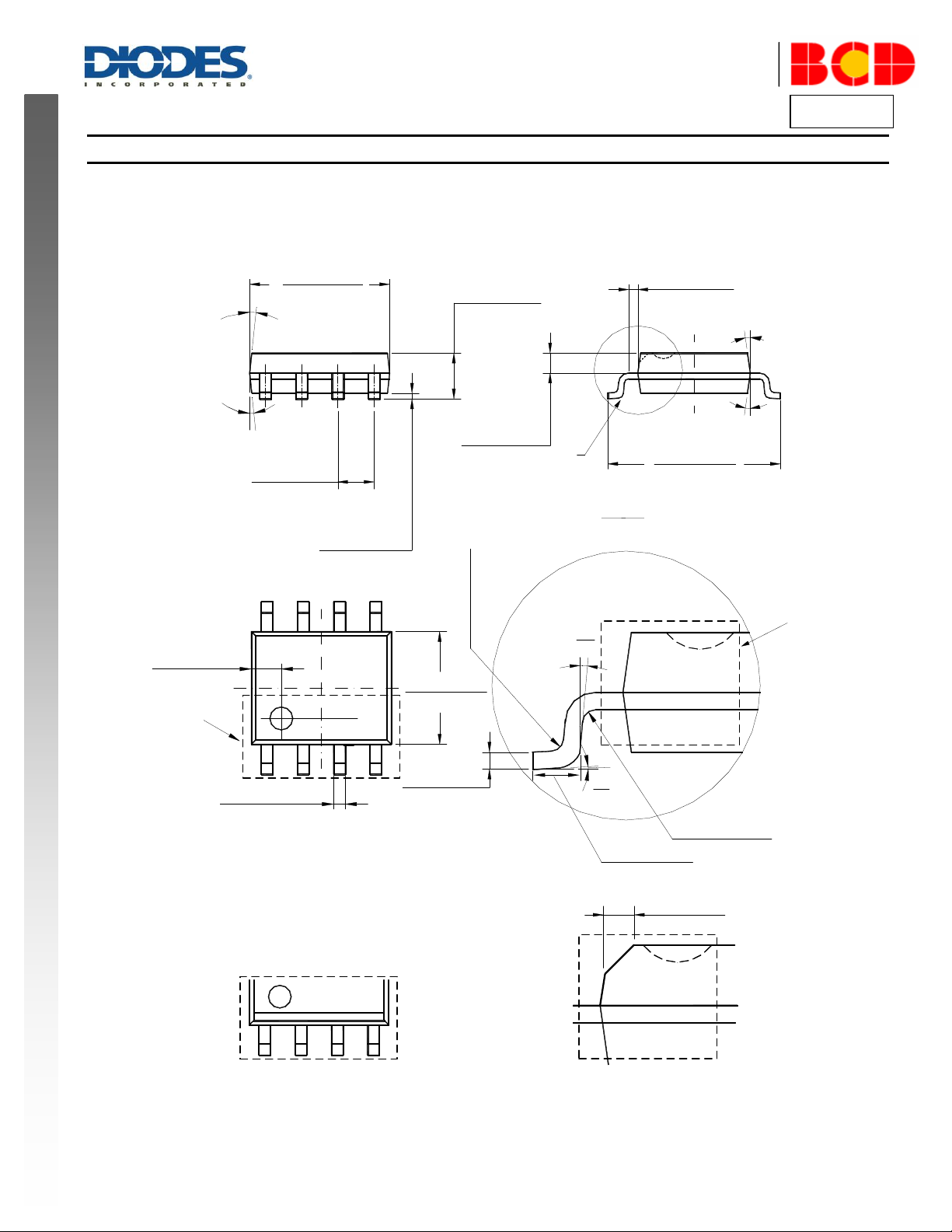
0
°
8
°
1
°
7
°
R
0
.
1
5
0
(
0
.
0
0
6
)
R0.150(0.006)
1.000(0.039)
0.300(0.012)
0.510(0.020)
1.350(0.053)
1.750(0.069)
0.100(0.004)
0.300(0.012)
3.800(0.150)
4.000(0.157)
7
°
7
°
20:
1
D
1.270(0.050)
TYP
0.150(0.006)
0.250(0.010)
8
°
D
5.800(0.228)
6.200(0.244)
0.600(0.024)
0.725(0.029)
0.320(0.013)
8
°
0.450(0.017)
0.820(0.032)
4.700(0.185)
5.100(0.201)
Note: Eject hole, oriented hole and mold mark is optional
.
Option 1
Option 1
Option 2
0.
350
(0.014)
TYP
TYP
TYP
9
°
~
9
°
~
Package Outline Dimensions (All dimensions in mm(inch).)
(1) Package Type: SO-8
Page 8

AP1690
Document number: DS36469 Rev. 2 - 2
8 of 9
www.diodes.com
May 2014
© Diodes Incorporated
AP1690
A Product Line of
Diodes Incorporated
NE W P R OD U C T
Grid
placement
courtyard
ZG
Y
E X
Dimensions
Z
(mm)/(inch)
G
(mm)/(inch)
X
(mm)/(inch)
Y
(mm)/(inch)
E
(mm)/(inch)
Value
6.900/0.272
3.900/0.154
0.650/0.026
1.500/0.059
1.270/0.050
Suggested Pad Layout
(1) Package Type: SO-8
Page 9
AP1690
Document number: DS36469 Rev. 2 - 2
9 of 9
www.diodes.com
May 2014
© Diodes Incorporated
AP1690
A Product Line of
Diodes Incorporated
NE W P R OD U C T
DIODES INCORPORATED MAKES NO WARRANTY OF ANY KIND, EXPRESS OR IMPLIED, WITH REGARDS TO THIS DOCUMENT,
INCLUDING, BUT NOT LIMITED TO, THE IMPLIED WARRANTIES OF MERCHANTABILITY AND FITNESS FOR A PARTICULAR PURPOSE
(AND THEIR EQUIVALENTS UNDER THE LAWS OF ANY JURISDICTION).
Diodes Incorporated and its subsidiaries reserve the right to make modifications, enhancements, improvements, corrections or other changes
without further notice to this document and any product described herein. Diodes Incorporated does not assume any liability arising out of the
application or use of this document or any product described herein; neither does Diodes Incorporated convey any license under its patent or
trademark rights, nor the rights of others. Any Customer or user of this document or products described herein in such applications shall assume
all risks of such use and will agree to hold Diodes Incorporated and all the companies whose products are represented on Diodes Incorporated
website, harmless against all damages.
Diodes Incorporated does not warrant or accept any liability whatsoever in respect of any products purchased through unauthorized sales channel.
Should Customers purchase or use Diodes Incorporated products for any unintended or unauthorized application, Customers shall indemnify and
hold Diodes Incorporated and its representatives harmless against all claims, damages, expenses, and attorney fees arising out of, directly or
indirectly, any claim of personal injury or death associated with such unintended or unauthorized application.
Products described herein may be covered by one or more United States, international or foreign patents pending. Product names and markings
noted herein may also be covered by one or more United States, international or foreign trademarks.
This document is written in English but may be translated into multiple languages for reference. Only the English version of this document is the
final and determinative format released by Diodes Incorporated.
Diodes Incorporated products are specifically not authorized for use as critical components in life support devices or systems without the express
written approval of the Chief Executive Officer of Diodes Incorporated. As used herein:
A. Life support devices or systems are devices or systems which:
1. are intended to implant into the body, or
2. support or sustain life and whose failure to perform when properly used in accordance with instructions for use provided in the
labeling can be reasonably expected to result in significant injury to the user.
B. A critical component is any component in a life support device or system whose failure to perform can be reasonably expected to cause the
failure of the life support device or to affect its safety or effectiveness.
Customers represent that they have all necessary expertise in the safety and regulatory ramifications of their life support devices or systems, and
acknowledge and agree that they are solely responsible for all legal, regulatory and safety-related requirements concerning their products and any
use of Diodes Incorporated products in such safety-critical, life support devices or systems, notwithstanding any devices- or systems-related
information or support that may be provided by Diodes Incorporated. Further, Customers must fully indemnify Diodes Incorporated and its
representatives against any damages arising out of the use of Diodes Incorporated products in such safety-critical, life support devices or systems.
Copyright © 2014, Diodes Incorporated
www.diodes.com
IMPORTANT NOTICE
LIFE SUPPORT
 Loading...