

Page 1
Single Stage Primary Side Regulation PFC Controller For LED Driver AP1682
Data Sheet
General Description
The AP1682 is a high performance AC/DC universal
input Primary Side Regulation Power Factor
Controller for LED driver applications. The device
uses Pulse Frequency Modulation (PFM) technology
to regulate output current while achieving high power
factor and low THD.
The AP1682 provides accurate constant current (CC)
regulation while removing the opto-coupler and
secondary control circuitry. It also eliminates the
need of loop compensation circuitry while
maintaining stability. The AP1682 achieves excellent
regulation and high efficiency, yet meets the
requirement of IEC61000-3-2 harmonic standard.
The AP1682 features low start-up current, low
operation current and high efficiency. It also has rich
protection features including over voltage, short
circuit, over current, over temperature p rotection etc.
The AP1682 is available in SOIC-8 package.
Features
• Primary Side Control for Output Current
Regulation Without Opto-coupler and Secondary
CV/CC Control Circuitry
• Low Start-up Current
• High Power Factor and Low THD for Universal
Input Range
• Tight CC Regulation Performance for Universal
Input Mains Voltage Range
• Eliminates Control Loop Compensation
Circuitry
• Built-in Acceleration Start
• Open-load and Reload Detection
• Over Voltage and Short Circuit Protection
• Over Temperature Protection
• Over Current Protection
• Cost Effective Total PFC LED Driver Solution
Applications
• Single Stage Power Factor Correction Power
Supply for LED Lighting
SOIC-8
Figure 1. Package Type of AP1682
Dec. 2011 Rev. 1. 1 BCD Semiconductor Manufacturing Limited
1
Page 2
Data Sheet
Single Stage Primary Side Regulation PFC Controller For LED Driver AP1682
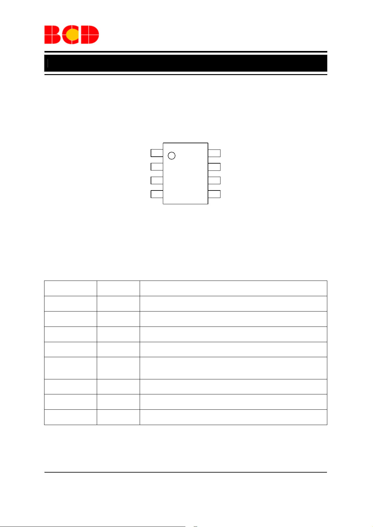
Pin Configuration
M Package
(SOIC-8)
NC
VS
8
1
2
VCC
7
OUT
VPK
CS
3
4
GND
6
5
FB
Figure 2. Pin Configuration of AP1682 (Top View)
Pin Description
Pin Number Pin Name Function
1
2
3
4
5
NC No connection
VS
VPK
CS Primary current sensing
FB
The rectified input voltage sensing pin. The pin is detecting the
instantaneous rectified sine waveform of input voltage
The rectified input voltage peak value sensing pin. The pin is detecting
the rectified sine waveform peak value of input voltage
This pin captures the feedback voltage from the auxiliary winding. FB
voltage is used to control no load output voltage and determine
acceleration stop point at start-up phase
6
7
8
GND Ground. Current return for gate driver and control circuits of the IC
OUT Gate driver output
VCC Supply voltage of gate driver and control circuits of the IC
Dec. 2011 Rev. 1. 1 BCD Semiconductor Manufacturing Limited
2
Page 3
Data Sheet
Single Stage Primary Side Regulation PFC Controller For LED Driver AP1682
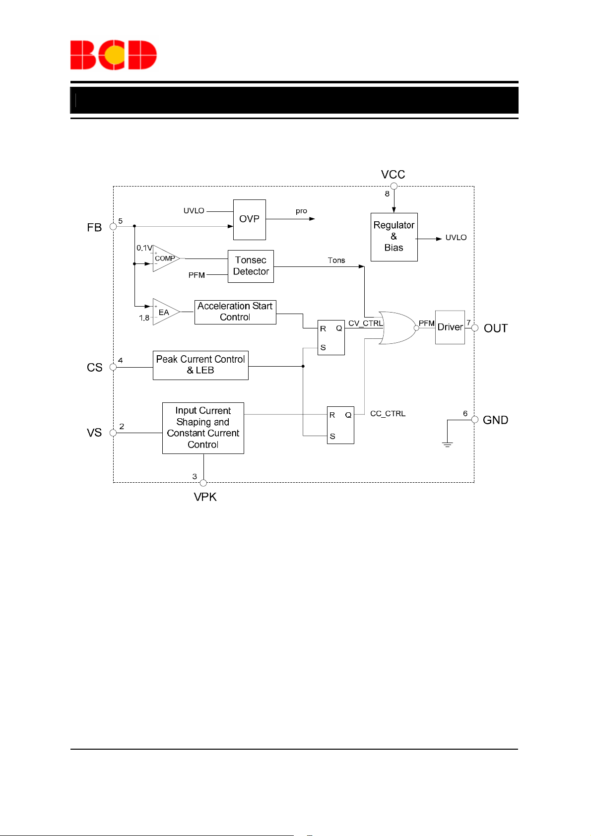
Functional Block Diagram
Figure 3. Functional Block Diagram of AP1682
Dec. 2011 Rev. 1. 1 BCD Semiconductor Manufacturing Limited
3
Page 4
Data Sheet
Single Stage Primary Side Regulation PFC Controller For LED Driver AP1682
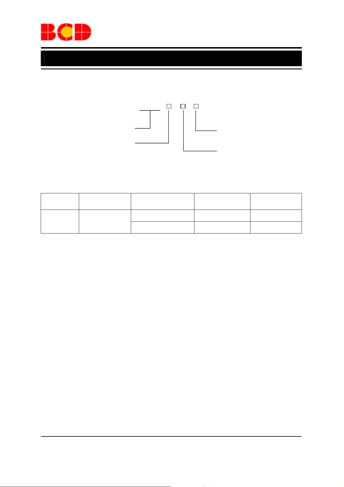
Ordering Information
AP1682 -
Package
Circuit Type
Package
M: SOIC-8
Temperature
Range
Part Number Marking ID Packing Type
G1: Green
TR: Tape & Reel
Blank: Tube
SOIC-8
-40 to 105°C
AP1682M-G1 1682M-G1 Tube
AP1682MTR-G1 1682M-G1 Tape & Reel
BCD Semiconductor's Pb-free products, as designated with "G1" suffix in the part number, are RoHS compliant
and green.
Dec. 2011 Rev. 1. 1 BCD Semiconductor Manufacturing Limited
4
Page 5

Data Sheet
Single Stage Primary Side Regulation PFC Controller For LED Driver AP1682
Absolute Maximum Ratings (Note 1)
Parameter Symbol Value Unit
Power Supply Voltage
Driver Output Current I
Voltage at VS, VPK, CS VVS, VPK, V
FB Input Voltage
Operating Junction Temperature TJ 150 ºC
Storage Temperature T
Lead Temperature (Soldering, 10 sec) T
Power Dissipation at TA=50°C
Thermal Resistance
(Junction-to-Ambient)
ESD (Machine Model) 200 V
ESD (Human Body Model) 3000 V
V
CC
300 mA
OUT
CS
V
FB
-65 to 150 ºC
STG
300 ºC
LEAD
0.65 W
P
D
θ
JA
-0.3 to 30 V
-0.3 to 7 V
-40 to 10 V
190
°C/W
Note 1: Stresses greater than those listed under “Absolute Maximu m Ratings” may cause permanent damage to
the device. These are stress ratings only, and functional operation of the device at these or any other conditions
beyond those indicated under “Recommended Operating Conditions” is not implied. Exposure to “Absolute
Maximum Ratings” for extended periods may affect device reliability.
Recommended Operating Conditions
Parameter Symbol Min Max Unit
Power Supply Voltage
Ambient Temperature TA -40 105 ºC
9 21 V
V
CC
Dec. 2011 Rev. 1. 1 BCD Semiconductor Manufacturing Limited
5
Page 6

Data Sheet
Single Stage Primary Side Regulation PFC Controller For LED Driver AP1682
Electrical Characteristics
V
=15V, TA=25°C, unless otherwise specified.
CC
Parameter Symbol Conditions Min Typ Max Unit
UVLO Section
Start-up Threshold VTH (ST)
Minimal Operating Voltage V
VCC OVP Voltage V
(Min) After turn on 7 8 9
OPR
28 32 36
CC_OVP
Standby Curr ent Section
Start-up Current IST
Maximum Operating
Current
(Max) VVS=VPK=3V 1000 1300
I
CC
V
CC=VTH
Before start up
(ST)-0.5V,
Drive Output Section
I
GD-SOURCE
V
CC
I
GD-SINK
V
CC
=1nF
L
=1nF
L
I
GD-SOURCE
V
CC
V
CC
I
SINK
Output High Level Voltage VOH
Output Low Level Voltage VOL
Output Voltage Rise Time tR C
Output Voltage Fall Time tF C
Output Clamp Voltage V
UVLO Saturation Voltage V
O-CLAMP
UVLO
=12V
=20mA
=12V
=20V
=0 to V
=10mA
=20mA
=5mA
CC–ON
VS Input Section
Maximum Ratio VVS/VPK (Max) VVS=VPK=3V 0.8 1 1.2 V
Minimu m Ratio VVS/VPK (Min) VVS=0V, VPK=3V 0.2 V
Current Sense Section
Minimu m On Time tON (Min) 500 750 1000 ns
Short Circuit Protection
Voltage
V
3 4 V
SOCP
Feedback Input Section
FB Pin Input Leakage
Current
Acceleration Start
Threshold
CV Threshold V
Over Voltage Protection V
I
V
FB
V
(ACC) 1.4 1.8 2.2 V
FB
(CV) 3.2 4.2 5.2 V
FB
(OVP) 4.5 6 7.5 V
FB
=4V 2 8
FB
Over Temperature Protection Section
Shutdown Temperature 140
Temperature Hysteresis 20
18 19 20
V
20
µA
10 V
1 V
100 140 190
30 60 90
ns
ns
12 13.5 15 V
1.1 V
µA
o
C
o
C
Dec. 2011 Rev. 1. 1 BCD Semiconductor Manufacturing Limited
6
Page 7

Data Sheet
Single Stage Primary Side Regulation PFC Controller For LED Driver AP1682
Typical Performance Characteristics
1100
1000
900
800
700
600
500
400
300
Supply Current (µA)
200
100
0
0 5 10 15 20 25 30
Figure 4. Supply Current vs. Supply Voltage Figure 5. CV Threshold Vs. Supply Voltage
14
13
12
11
10
Output Clamp Voltage (V)
Dec. 2011 Rev. 1. 1 BCD Semiconductor Manufacturing Limited
9
8
7
6
5
8 1012141618202224262830
Figure 6. Output Clamp Voltage vs. Figure 7. Start-up Voltage vs.
Supply Voltage Ambient Temperature
Supply Voltage (V)
Supply Voltage (V)
4.2
4.0
3.8
CV Threshold (V)
3.6
8 1012141618202224262830
Supply Voltage (V)
19.4
19.2
19.0
18.8
18.6
Start-up Voltage (V)
18.4
18.2
18.0
-40 -20 0 20 40 60 80 100 120
Ambient Temperature (oC)
7
Page 8

Data Sheet
Single Stage Primary Side Regulation PFC Controller For LED Driver AP1682
Typical Performance Characteristics (Continued)
8.3
8.2
8.1
8.0
7.9
Minimal Operating Voltage (V)
7.8
-40 -20 0 20 40 60 80 100 120
Ambient Temperature (oC)
8.0
7.5
7.0
6.5
6.0
5.5
5.0
4.5
4.0
Start-up Current (µA)
3.5
3.0
2.5
2.0
-40 -20 0 20 40 60 80 100 120
Ambient Temperature (oC)
Figure 8. Minimal Operating Voltage vs. Figure 9. Start-up Current vs. Ambient T emperature
Ambient Temperature
1050
1000
950
900
850
Operating Current (µA)
800
-40 -20 0 20 40 60 80 100 120
Ambient Temperature (oC)
4.50
4.25
4.00
3.75
3.50
CV Threshold (V)
3.25
3.00
-40 -20 0 20 40 60 80 100 120
Ambient Temperature (oC)
Figure 10. Operating Current vs. Figure 11. CV Threshold Vs.
Ambient Temperature Ambient Temperature
Dec. 2011 Rev. 1. 1 BCD Semiconductor Manufacturing Limited
8
Page 9

Data Sheet
Single Stage Primary Side Regulation PFC Controller For LED Driver AP1682
Typical Performance Characteristics (Continued)
3.0
2.5
2.0
1.5
FB Input Leakage Current (µA)
1.0
-40-20 0 20406080100120
Ambient Temperature (oC)
Figure 12. FB Input Leakage Current vs.
Ambient Temperature
Typical Application
Figure 13. Typical Application of AP1682
Dec. 2011 Rev. 1. 1 BCD Semiconductor Manufacturing Limited
9
Page 10

Data Sheet
Single Stage Primary Side Regulation PFC Controller For LED Driver AP1682
Mechanical Dimensions
SOIC-8 Unit: mm(inch)
R0.150(0.006)
Dec. 2011 Rev. 1. 1 BCD Semiconductor Manufacturing Limited
10
Page 11

BCD Semiconductor Manufacturing Limited
IMPORTANT NOTICE
IMPORTANT NOTICE
BCD Semiconductor Manufacturing Limited reserves the right to make changes without further notice to any products or specifi-
BCD Semiconductor Manufacturing Limited reserves the right to make changes without further notice to any products or specifi-
cations herein. BCD Semiconductor Manufacturing Limited does not assume any responsibility for use of any its products for any
cations herein. BCD Semiconductor Manufacturing Limited does not assume any responsibility for use of any its products for any
particular purpose, nor does BCD Semiconductor Manufacturing Limited assume any liability arising out of the application or use
particular purpose, nor does BCD Semiconductor Manufacturing Limited assume any liability arising out of the application or use
of any its products or circuits. BCD Semiconductor Manufacturing Limited does not convey any license under its patent rights or
of any its products or circuits. BCD Semiconductor Manufacturing Limited does not convey any license under its patent rights or
other rights nor the rights of others.
other rights nor the rights of others.
http://www.bcdsemi.com
MAIN SITE
MAIN SITE
- Headquarters
BCD Semiconductor Manufacturing Limited
BCD Semiconductor Manufactur ing Limited
- Wafer Fab
No. 1600, Zi Xing Road, Shanghai ZiZhu Science-based Industrial Park, 200241, China
Shanghai SIM-BCD Semiconductor Manufacturing Limited
Tel: +86-21-24162266, Fax: +86-21-24162277
800, Yi Shan Road, Shanghai 200233, China
Tel: +86-21-6485 1491, Fax: +86-21-5450 0008
REGIONAL SALES OFFICE
Shenzhen Office
REGIONAL SALES OFFICE
Shanghai SIM-BCD Semiconductor Manufacturing Co., Ltd., Shenzhen Office
Shenzhen Office
Unit A Room 1203, Skyworth Bldg., Gaoxin Ave.1.S., Nanshan District, Shenzhen,
Shanghai SIM-BCD Semiconductor Manufacturing Co., Ltd. Shenzhen Office
China
Advanced Analog Circuits (Shanghai) Corporation Shenzhen Office
Tel: +86-755-8826 7951
Room E, 5F, Noble Center, No.1006, 3rd Fuzhong Road, Futian District, Shenzhen 518026, China
Fax: +86-755-8826 7865
Tel: +86-755-8826 7951
Fax: +86-755-8826 7865
- Wafer Fab
BCD Semiconductor Manufacturing Limited
Shanghai SIM-BCD Semiconductor Manufacturing Co., Ltd.
- IC Design Group
800 Yi Shan Road, Shanghai 200233, China
Advanced Analog Circuits (Shanghai) Corporation
Tel: +86-21-6485 1491, Fax: +86-21-5450 0008
8F, Zone B, 900, Yi Shan Road, Shanghai 200233, China
Tel: +86-21-6495 9539, Fax: +86-21-6485 9673
Taiwan Office
BCD Semiconductor (Taiwan) Company Limited
Taiwan Office
4F, 298-1, Rui Guang Road, Nei-Hu District, Taipei,
BCD Semiconductor (Taiwan) Company Limited
Tai wan
4F, 298-1, Rui Guang Road, Nei-Hu District, Taipei,
Tel: +886-2-2656 2808
Taiwan
Fax: +886-2-2656 2806
Tel: +886-2-2656 2808
Fax: +886-2-2656 2806
USA Office
BCD Semiconductor Corp.
USA Office
30920 Huntwood Ave. Hayward,
BCD Semiconductor Corporation
CA 94544, USA
30920 Huntwood Ave. Hayward,
Tel : +1-510-324-2988
CA 94544, U.S.A
Fax: +1-510-324-2788
Tel : +1-510-324-2988
Fax: +1-510-324-2788
 Loading...