

Page 1
AP1539
18V 4A 300KHz BUCK CONVERTER
Features
• Input voltage: 3.6V to 18V
• Output voltage: 0.8V to V
• Output current: up to 4A
• Duty ratio: 0% to 99% PWM control
• Oscillation frequency: 300KHz typ.
• Soft-start like, Current limit and Enable function
• Thermal Shutdown function
• Built-in internal SW P-channel MOS
• SOP-8L-DEP: Available in “Green” Molding Compound
(No Br, Sb)
• Lead Free Finish / RoHS Compliant (Note 1)
CC
Applications
• PC Motherboard
• LCD Monitor
• Graphic Card
• DVD-Video Player
• Telecom Equipment
• ADSL Modem
• Printer and other Peripheral Equipment
• Microprocessor core supply
General Description
AP1539 consists of step-down switching regulator with PWM
control. These devices include a reference voltage source,
oscillation circuit, error amplifier, internal PMOS.
AP1539 provides low-ripple power, high efficiency, and excellent
transient characteristics. The PWM control circuit is able to vary
the duty ratio linearly from 0 up to 99%. This converter also
contains an error amplifier circuit as well as a soft-start circuit that
prevents overshoot at startup. An enable function, an over
current protect function and a short circuit protect function are built
inside, and when OCP or SCP happens, the operation frequency
will be reduced from 300KHz to 50KHz. Also, an internal
compensation block is built in to minimum external component
count. With the addition of an internal P-channel Power MOS, a
coil, capacitors, and a diode connected externally, these ICs can
function as step-down switching regulators. They serve as ideal
power supply units for portable devices when coupled with the
SOP-8L-DEP mini-package, providing such outstanding features
as low current consumption. Since this converter can
accommodate an input voltage up to 18V, it is also suitable for the
operation via an AC adapter.
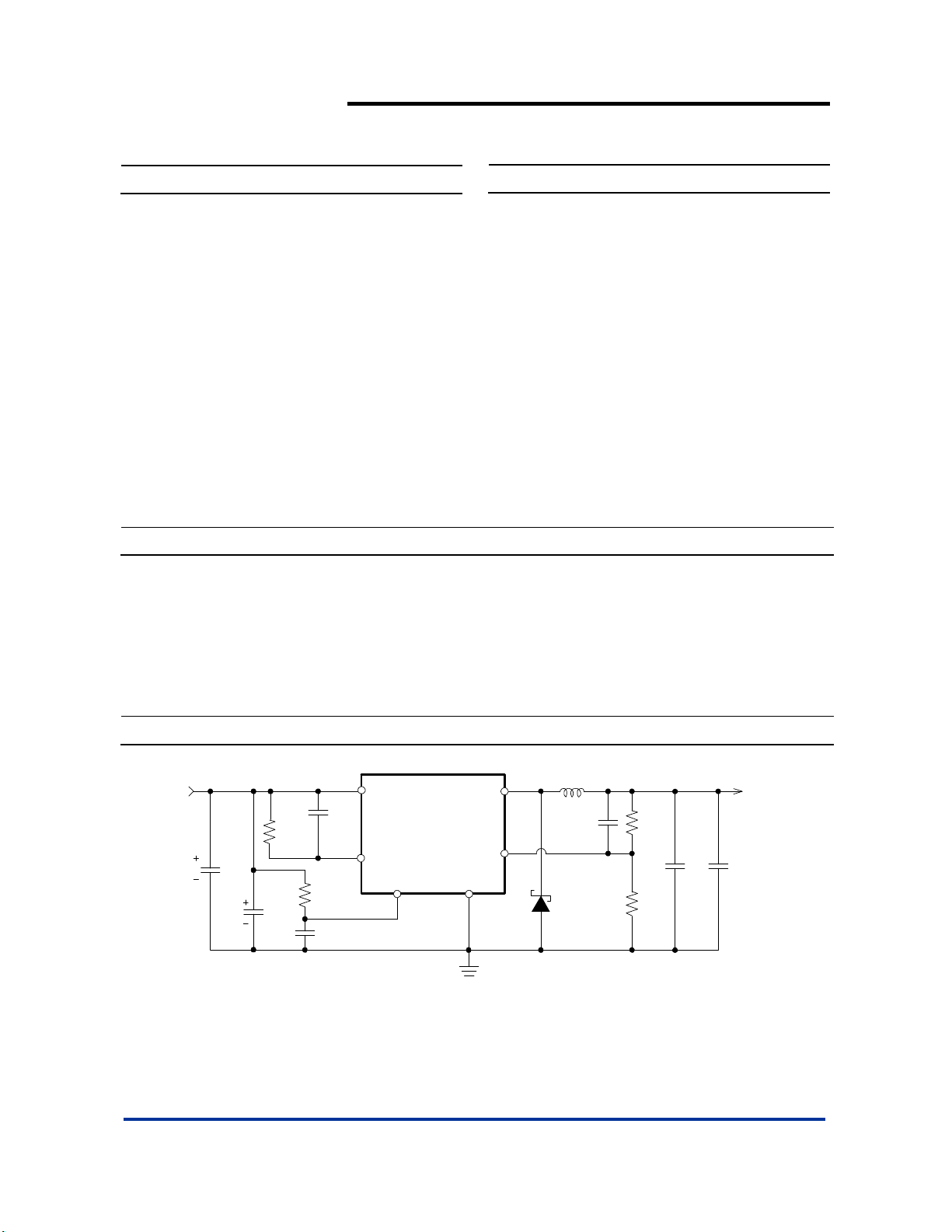
Typical Application Circuit
V
= 5V/4A
+
-
OUT
C
0.1uF
+
C
OUT
470uF
-
***
V
IN
R
OCSET
Option
3.9K
C
IN
470uF
CVcc
0.1uF
Notes: * Typical feedback compensation (Cc): 5600pF.
** Suggested DIODES Power Schottky P/N: B540 series or PDS540.
R
100K
C
0.1uF
*** Suggested C
C
EN
EN
OCSET
Vcc
AP 1539
OCSET
EN
V
V
OUT
=
= 0.7K~5K ohm
R
B
for V
OUT
OUT
x (
1+
FB
< 1V; 680uF.
Output
FB
V
SS
R
A
/R
)
B
L1
22uH
Cc
Option*
D1**
R
A
6.8K
R
B
1.3K
AP1539 Rev. 4 1 of 13 OCTOBER 2009
DS31477 www.diodes.com © Diodes Incorporated
Page 2
Ordering Information
AP 1539 SDP G - 13
Package PackingGreen
AP1539
18V 4A 300KHz BUCK CONVERTER
SDP : SOP-8L-DEP
Device
AP1539SDPG-13 SDP SOP-8L-DEP 2500/Tape & Reel -13
Notes: 1. EU Directive 2002/95/EC (RoHS). All applicable RoHS exemptions applied. Please visit our website at
http://www.diodes.com/datasheets/ap02001.pdf.
http://www.diodes.com/products/lead_free.html
2. Pad layout as shown on Diodes Inc. suggested pad layout document AP02001, which can be found on our website at
Package
Code
Packaging
(Note 2)
G : Green
Quantity Part Number Suffix
13 : Tape & Reel
13” Tape and Reel
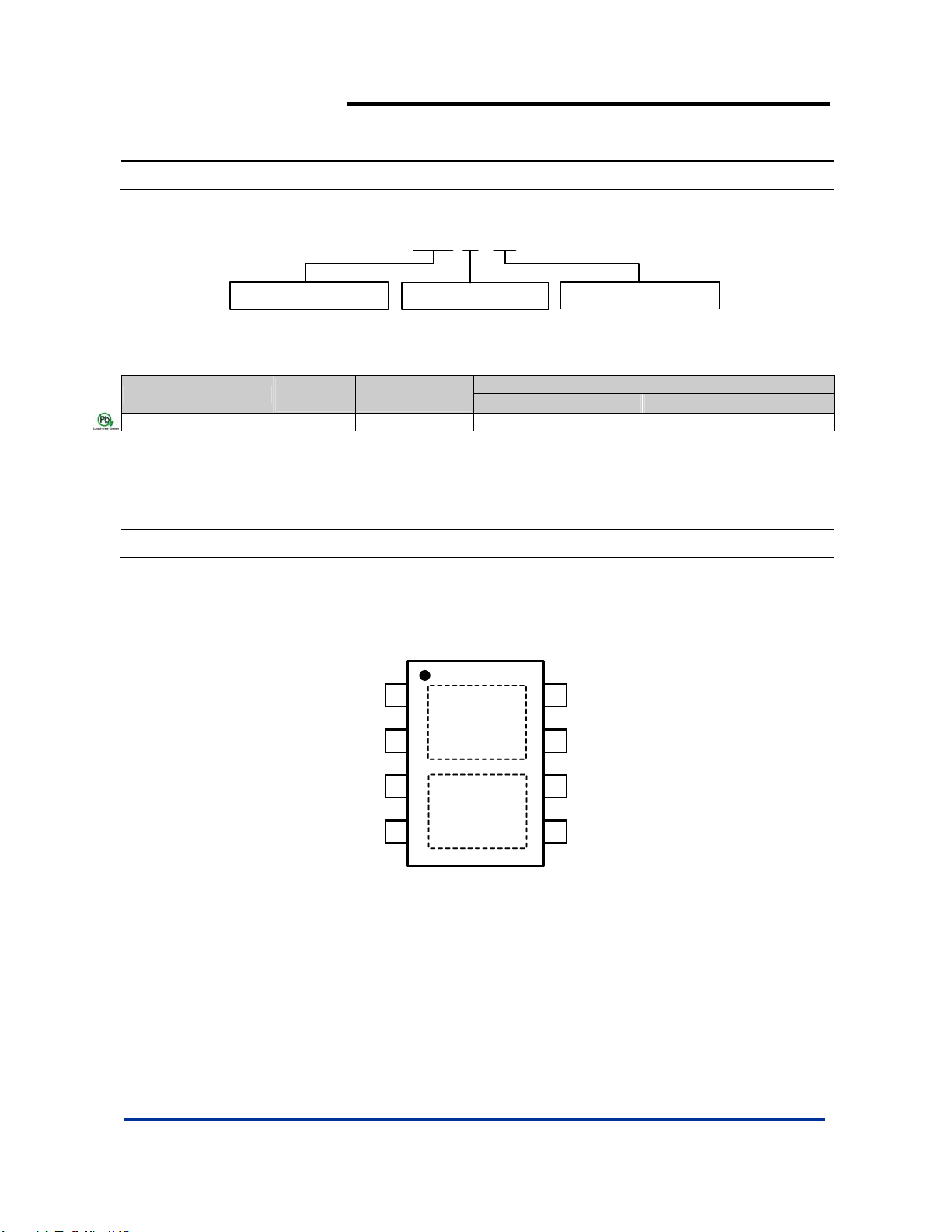
Pin Assignments
SOP-8L-DEP (Dual Exposed Pads)
( Top View )
FB
1
Vss
8
1
EN
2
Vss
7
OCSET
3
6
Output
2
4
V
CC
Notes: 3. Exposed pad 1 is connected to VSS and exposed pad 2 is connected to Output. The board layout for exposed pads needs to be considered to
AP1539 Rev. 4 2 of 13 OCTOBER 2009
DS31477 www.diodes.com © Diodes Incorporated
avoid short circuit.
(Note 3)
5
Output
Page 3
18V 4A 300KHz BUCK CONVERTER
Pin Descriptions
Pin Name
FB 1 Feedback pin
EN 2
OCSET 3 Add an external resistor to set max output current
VCC 4 IC power supply pin
Pin No.
Power-off pin
H: Normal operation (Step-down operation)
L: Step-down operation s t op p e d (A l l ci rc ui ts de ac t i v a te d)
Description
AP1539
Output 5, 6
VSS 7, 8 GND Pin
Switch Pin. Connect external inductor/diode here. Minimize trace area
at this pin to reduce EMI
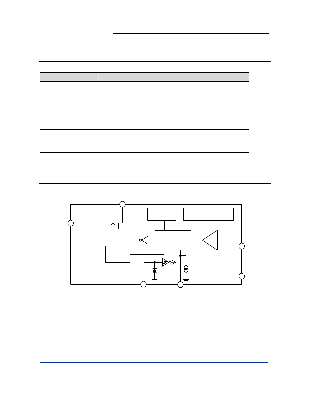
Block Diagram
Output
Osci ll ation
Circuit
Vcc
PWM-Switched
Contro l Circuit
Thermal
Shutdown
EN
EN
AP1539 Rev. 4 3 of 13 OCTOBER 2009
DS31477 www.diodes.com © Diodes Incorporated
Reference Voltage
Source with Soft S tart
+
-
90uA
OCSET
FB
VssV
Page 4
A
AP1539
18V 4A 300KHz BUCK CONVERTER
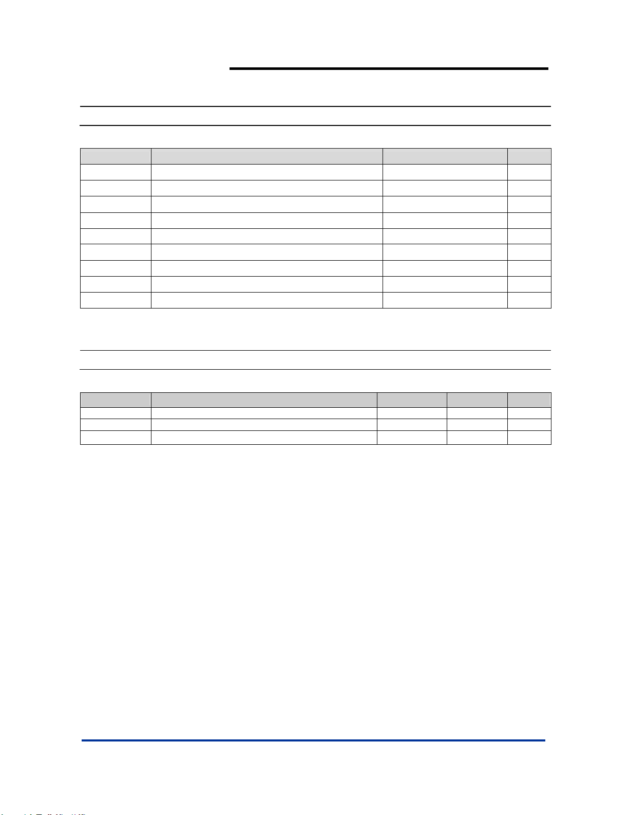
Absolute Maximum Ratings
Symbol Parameter Rating Unit
ESD HBM Human Body Model ESD Protection 5.5 KV
ESD MM Machine Model ESD Protection 200 V
VCC VCC Pin Voltage VSS - 0.3 to VSS + 20 V
VFB Feedback Pin Voltage VSS - 0.3 to VCC V
VEN EN Pin Voltage VSS - 0.3 to VCC V
V
Switch Pin Voltage VSS - 0.3 to VCC V
OUT
PD Power Dissipation Internally limited mW
TJ Operating Junction Temperature Range -40 to +125
T
Storage Temperature Range -65 to +150
ST
Caution: The absolute maximum ratings are rated values exceeding which the product could suffer physical damage.
These values must therefore not be exceeded under any conditions.
Recommended Operating Conditions
Symbol Parameter Min Max Unit
VIN Input Voltage (Note 4) 3.6 18 V
I
Output Current 0 4
OUT
TA Operating Ambient Temperature
Notes: 4. For the operations in low input voltage, AP1539 can tolerate down to 3.6V but max output current loading will be less than 4A. For nominal
applications in such low input voltage range, especially lower than 4V, a higher ROCSET with larger heat sink is recommended.
AP1539 Rev. 4 4 of 13 OCTOBER 2009
DS31477 www.diodes.com © Diodes Incorporated
-20 +85
o
C
o
C
o
C
Page 5
A
AP1539
18V 4A 300KHz BUCK CONVERTER
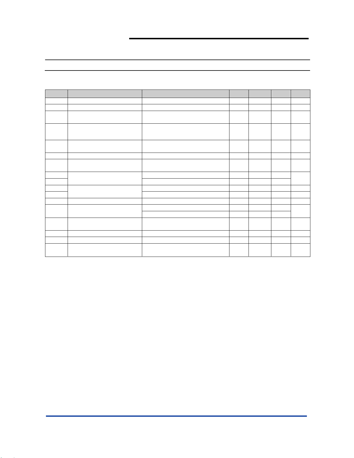
Electrical Characteristics
IN = 12V, T
(V
Symbol Parameter Conditions Min Typ. Max Unit
VFB Feedback Voltage I
IFB Feedback Bias Current I
I
SHDN
∆V
OUT
/ VIN
∆V
OUT
/ V
OUT
f
Oscillation Frequency Measure waveform at SW pin 240 300 400 KHz
OSC
f
OSC1
VIH
VIL Evaluate oscillation stop at SW pin - - 0.8
ISH
ISL EN Pin Low - -10 - µA
I
OCSET
R
DS(ON)
EFFI Efficiency
T
SHDN
T
Thermal shutdown hysteresis - 55 - °C
HYS
θ
JC
Notes: 5. Test condition for SOP-8L-DEP: Devices mounted on 2oz copper, minimum recommended pad layout on top & bottom layer with thermal vias,
= 25°C, unless otherwise specified)
A
= 0.1A 0.784 0.8 0.816 V
OUT
= 0.1A - 0.1 0.5 µA
OUT
Current Consumption During
Power Off
Line Regulation V
Load Regulation I
Frequency of Current Limit or
Short Circuit Protection
EN Pin Input Voltage
EN Pin Input Leakage Current
V
= 0V - 10 - µA
EN
= 5V~18V - 1 2 %
IN
= 0.1 to 4A - 0.2 0.5 %
OUT
Measure waveform at SW pin - 50 - KHz
Evaluate oscillation at SW pin 2.0 - -
V
EN Pin High - 20 - µA
OCSET Pin Bias Current -- 7 5 90 105 µA
Internal MOSFET R
DS(ON)
= 5V, V
V
IN
VIN= 12V, V
V
= 12V, V
IN
I
=4
OUT
= 0V - 90 -
FB
= 0V - 50 -
FB
= 5V
OUT
- 92 - %
mΩ
Thermal shutdown threshold - 150 - °C
Thermal Resistance
Junction-to-Case
double sided FR-4 PCB.
SOP-8L-DEP (Note 5) - 26 -
o
C/W
AP1539 Rev. 4 5 of 13 OCTOBER 2009
DS31477 www.diodes.com © Diodes Incorporated
Page 6
AP1539
18V 4A 300KHz BUCK CONVERTER
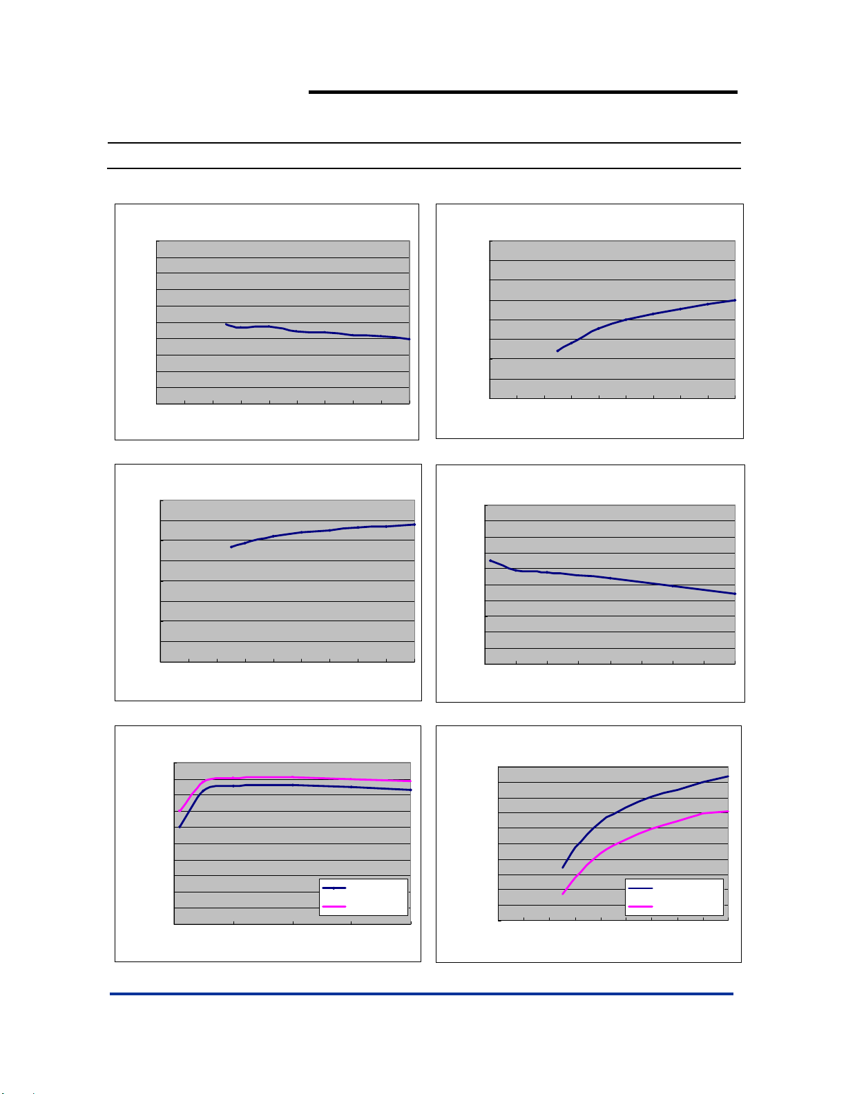
Typical Performance Characteristics
VIN v s. Frequency
(V
= 3.3V, I
326
OUT
324
322
320
318
316
(kHz)
OSC
314
F
312
310
308
306
024681012141618
= 0.2A)
OUT
0.820
0.815
0.810
0.805
(V)
0.800
FB
V
0.795
0.790
0.785
0.780
0 2 4 6 8 10 12 14 16 18
(V)
V
IN
Line Regulation
(V
= 3.3V, I
3.40
OUT
3.35
3.30
3.25
(V)
3.20
OUT
V
3.15
3.10
3.05
3.00
024681012141618
= 0.2A)
OUT
3.35
3.34
3.33
3.32
3.31
(V)
3.30
OUT
3.29
V
3.28
3.27
3.26
3.25
(V)
V
IN
0.0 0.5 1.0 1.5 2.0 2.5 3.0 3.5 4.0
Efficiency
(V
= 12V)
100
90
80
70
60
50
40
Efficiency (%)
30
20
10
0
0.0 1.0 2.0 3.0 4.0
IN
7.5
7.0
6.5
6.0
5.5
5.0
4.5
4.0
VOUT=3.3V
VOUT=5V
Current Limit (A)
3.5
3.0
2.5
0 2 4 6 8 10 12 14 16 18
(A)
I
OUT
AP1539 Rev. 4 6 of 13 OCTOBER 2009
DS31477 www.diodes.com © Diodes Incorporated
(V
OUT
VIN vs. V
= 3.3V, I
FB
= 0.2A)
OUT
(V)
V
IN
Load Regulation
(V
= 12V)
IN
I
(A)
OUT
Swit c h Cur r e nt Limit
(TA = 25℃)
(V)
V
IN
ROCSET=6.8k
ROCSET=4.7k
Page 7
V
V
18V 4A 300KHz BUCK CONVERTER
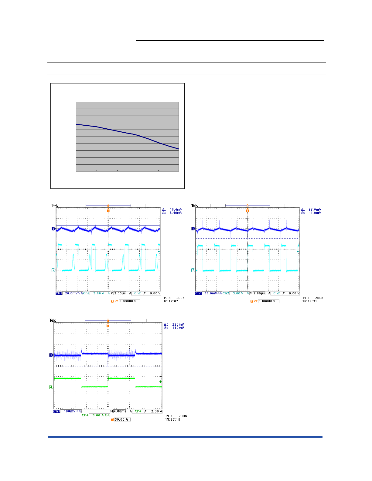
Typical Performance Characteristics (Continued)
Current Limit vs. Temperature
(V
= 12V, R
9.0
8.5
8.0
7.5
7.0
6.5
6.0
5.5
Current Limit (A)
5.0
4.5
4.0
-25 0 25 50 75 100
IN
Ambient Temperature (C)
OCSET
= 6.8k)
AP1539
Ripple
(V
IN
=12V, V
OUT
=3.3V, I
OUT
Load Transient Response
(V
IN
=12V, V
=3.3V, I
OUT
=0.1A)
OUT
=0.1~4A)
OUT
(V
IN
=12V, V
OUT
OUT
Ripple
=3.3V, I
OUT
=4.0A)
AP1539 Rev. 4 7 of 13 OCTOBER 2009
DS31477 www.diodes.com © Diodes Incorporated
Page 8
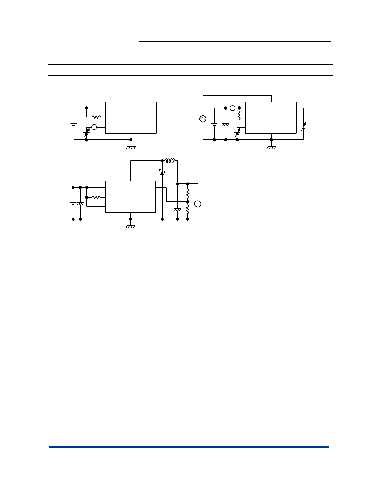
Test Circuit
18V 4A 300KHz BUCK CONVERTER
open
OUTPUT OUTPUT
CC
OCSET
A
EN
V
SS
Enable function test Feedback function test
open
FBV
Oscillation
A
V
CC
+
-
OCSET
EN
V
AP1539
FB
SS
V
CC
+
-
OCSET
EN
Operation function test
OUTPUT
FB
V
V
SS
+
-
AP1539 Rev. 4 8 of 13 OCTOBER 2009
DS31477 www.diodes.com © Diodes Incorporated
Page 9
AP1539
18V 4A 300KHz BUCK CONVERTER
Functional Descriptions
PWM Control
The AP1539 is a DC/DC converter that employs pulse width
modulation (PWM) scheme. Its pulse width varies in the range of
0% to 99%, based on the output current loading. The output
ripple voltage caused by the PWM high frequency switching can
easily be reduced through an output filter. Therefore, this
converter provides a low ripple output supply over a broad range
of input voltage & output current loading
Under Voltage Lockout
The under voltage lockout circuit of the AP1539 assures that the
high-side MOSFET driver remains in the off state whenever the
supply voltage drops below 3.3V. Normal operation resumes
once V
Current Limit Protection
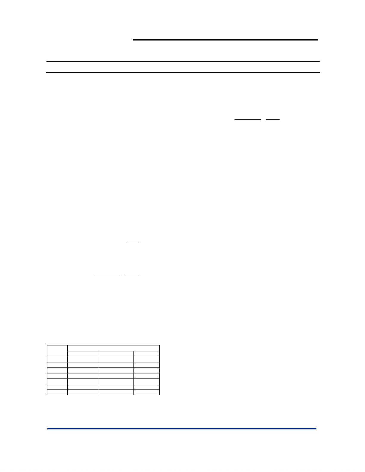
The current limit threshold is set by external resistor R
connected from V
current I
at OCSET pin. When the PWM voltage is less than the voltage at
OCSET, an over-cur rent condition is triggered.
The current limit threshold is given by the following equation:
where,
I
resistance; F
inductor value will affect the ripple current ΔI.
The above equation is recommended for input voltage range of
5V to 18V. For input voltage lower than 5V, higher than 18V or
ambient temperature over 100°C, higher R
recommended.
The recommended minimum R
rises above 3.5V.
CC
supply to OCSET pin. The internal sink
CC
(90uA typical) across this resistor sets the voltage
OCSET
×=×
RIRI
OCSETOCSETDS(ON)PEAK
)I(Δ
+>
II
OUT(MAX)PEAK
VV
−
I ×
=Δ
is the output peak current; R
PEAK
V
OUT
(V)
0.8 6.8K 3.9K 4.7K
1.0 6.8K 3.9K 4.7K
1.2 6.8K 3.9K 4.7K
1.8 6.8K 3.9K 4.7K
2.5 6.8K 3.9K 4.7K
3.3 6.8K 3.9K 4.7K
5.0 N/A 3.9K 5.6K
is the PWM frequency (300KHz typical). Also, the
S
5V 12V 18V
Lfs
×
DS (ON)
value is summarized below:
OCSET
VIN (V)
2
V
OUTOUTIN
V
IN
is the MOSFET ON
OCSET
OCSET
is
AP1539 Rev. 4 9 of 13 OCTOBER 2009
DS31477 www.diodes.com © Diodes Incorporated
Inductor Selection
For most designs, the operates with inductors of 22µH to
33µH. The inductor value can be derived from the following
equation:
VV
L ×
Where ΔI
ripple current and small value inductors result in high ripple
current. Choose inductor ripple current approximately 15% of the
maximum load current 4A, ∆I
inductor should be at least equal to the maximum load current
plus half the ripple current to prevent core saturation (4A+0.3A).
Input Capacitor Selection
This capacitor should be located close to the IC using short leads
and the voltage rating should be approximately 1.5 times the
maximum input volta ge. The RMS current rati ng requirement for
the input capacitor of a buck regulator is approximately 1⁄2 the
DC load current. A low ESR input capacitor sized for maximum
RMS current must be used. A 470µF low ESR capacito r for most
applications is sufficient.
Output Capacitor Selection
The output capacitor is required to filter the output voltage and
provides regulator loop stability. The important capacitor
parameters are the 100KHz Equivalent Series Resistance (ESR),
the RMS ripples current rating, voltage rating and capacitance
value. For the output capacitor, the ESR value is the most
important parameter . The output ripple can be calculated fro m
the following formula.
The bulk capacitor’s ESR will determine the output ripple voltage
and the initial voltage drop after a high slew-rate transient.
An aluminum electrolytic capacitor's ESR value is related to the
capacitance and its voltage rating. In most case, higher voltage
electrolytic capacitors have lower ESR values. Most of the time,
capacitors with much higher voltage ratings may be needed to
provide the low ESR values required for low output ripple v oltage .
PCB Layout Guide
If you need low T
SW pins(5& 6) and Vss pins(7& 8)on the SOP-8L package are
internally connected to die pad, The evaluation board should be
allowed for maximum copper area at output (SW) pins.
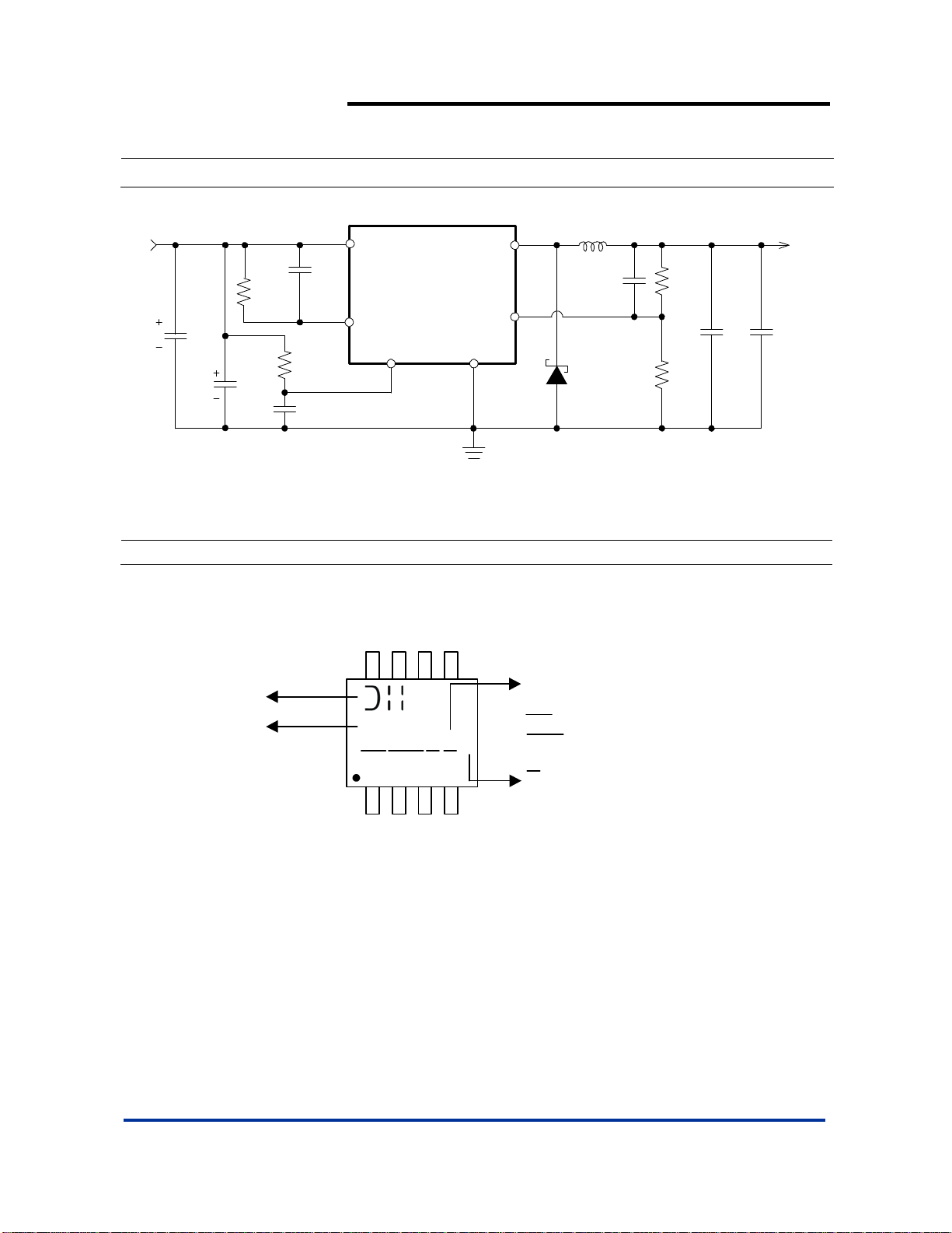
1. Connect FB circuits (R
2. Connect C3 to Vcc and Vss pin as closely as possible to get
3. Connect R4 to Vcc and OCSET pin as closely as possible.
4. Connect ground side of the C2 & D1 & C4 as closely as
is inductor Ripple Current. Large value inductors lower
L
& TJ or large PD (Power Dissipation), The dual
C
keep away from inductor flux for pure V
good power filter effect.
possible and use ground plane for best performance.
−
=
fs
=0.6A. The DC current rating of the
L
, R2, C1) as closely as possible and
1
V
OUTOUTIN
Δ×
V
I
ΔIV
LRIPPLE
×=
IN
ESR
FB
.
Page 10
V
Functional Description (Continued)
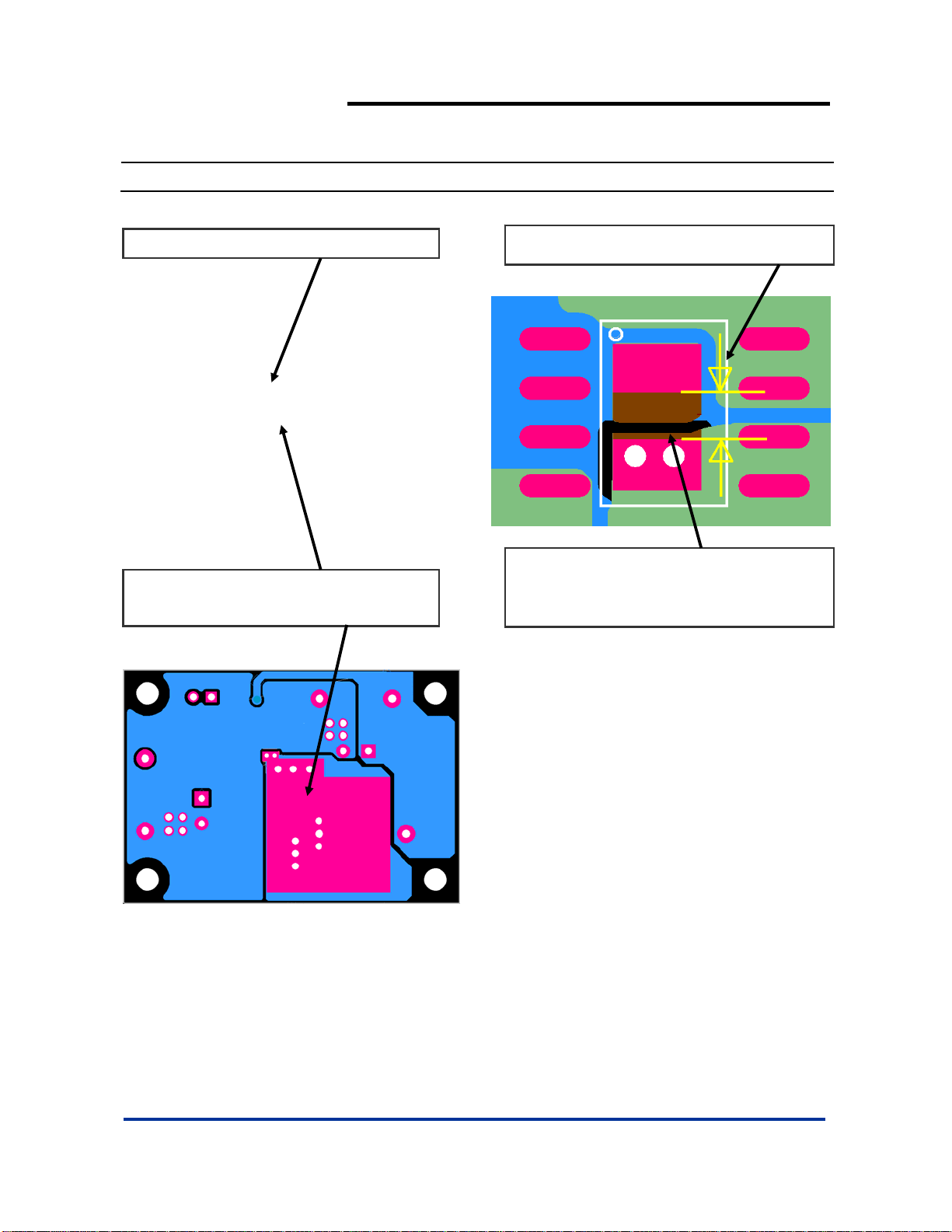
Keep the gap of exposed pads from short circui t.
Top Side Layout Guid e
AP1539
18V 4A 300KHz BUCK CONVERTER
Recommended exposed-pads gap: 30~40mil
(0.75~1mm)
Use vias to conduct the heat into the backside of
PCB layer. The heat si nk at output (SW) pins should
be allowed for maximum solder-painted area.
Bottom Side Layout Guide
Brown: IC exposed pads.
Red: recommended layout.
Reference pads layout dimension:
Output: 90 x 50 mil
ss: 90 x 60 mil
AP1539 Rev. 4 10 of 13 OCTOBER 2009
DS31477 www.diodes.com © Diodes Incorporated
Page 11
Functional Description (Continued)
V
IN
Vcc
Output
AP1539
18V 4A 300KHz BUCK CONVERTER
L1
V
OUT
R4
C2
C3
C7
Option
R5
C6
Marking Information
(1) SOP-8L-DEP
Logo
Part No.
AP1539
OCSET
EN
Figure: Layout numbering comparison.
FB
V
SS
C1
Option
D1
( Top View )
8
5
G : Green
: Year : 08, 09,10~
YY
AP1539
WW X
YY
X
E
WW
: Week : 01~52; 52
represents 52 and 53 week
X
: Internal Code
SOP-8L-DEP
41
R1
R2
C8
+
C4
-
+
-
AP1539 Rev. 4 11 of 13 OCTOBER 2009
DS31477 www.diodes.com © Diodes Incorporated
Page 12
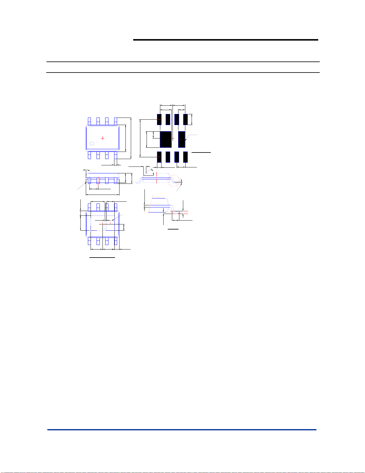
Package Information (All Dimensions in mm)
(1) Package type: SOP-8L-DEP
8
5
8
C
L
1.8 1.8
0.951.65
5
8x-1.55
AP1539
18V 4A 300KHz BUCK CONVERTER
1.0
C
L
5.4
3.85/3.95
2.35
5.90/6.10
EXPOSED PAD
Top View
9
1
.
0
R
0.685
2.15Typ.
i
s
l
l
a
(
°
1
0.3/0.5
)
e
d
1.27Typ.
4.85/4.95
2.05Typ.
1
0.20
1.7 1. 7
C
L
Bottom view
4
1.15Typ.
4
58
0.35Typ.
1.4/1.5
EXPOSED PAD
C
L
0.9
0.713
1
8x-0.60
4
5
°
1.63Max.
View"A"
0.15/0.25
0/0.13
View"A"
0
8
/
°
°
0.254
0.62/0.82
Land Pattem Recommendation
(Unit: mm)
4
6x-1.27
Gauge Plane
Seating Plane
AP1539 Rev. 4 12 of 13 OCTOBER 2009
DS31477 www.diodes.com © Diodes Incorporated
Page 13

AP1539
18V 4A 300KHz BUCK CONVERTER
DIODES INCORPORATED MAKES NO WARRANTY OF ANY KIND, EXPRESS OR IMPLIED, WITH REGARDS TO THIS
DOCUMENT, INCLUDING, BUT NOT LIMITED TO, THE IMPLIED WARRANTIES OF MERCHANTABILITY AND FITNESS FOR A
PARTICULAR PURPOSE (AND THEIR EQUIVALENTS UNDER THE LAWS OF ANY JURISDICTION).
Diodes Incorporated and its subs idiaries reserve the right to make modific ations, enhancem ents, improvem ents, correctio ns or other
changes without further notic e to this document and any product des cri bed herein. Diodes Inc orporat ed does not assum e any liabi lity
arising out of the applicati on or use of this document or any produc t described herein ; neither does Diodes In corporat ed convey any
license under its patent or trademark rights, nor the rights of others . Any Customer or user of t his document or produc ts described
herein in such applications shall assume all risks of such use and will agree to hold Diodes Incorporated and all the companies
whose products are represented on Diodes Incorporated website, harmless against all damages.
Diodes Incorporated do es not warrant or accept an y liabilit y whatsoever in re spect of any product s purchased through unaut horized
sales channel.
Should Customers purchase or use Diod es Incorporated products for any unintend ed or unauthorized application, Custom ers shall
indemnify and hold Diodes Incorpor ated and its repres entatives harmless agai nst all claims, damages , expenses, and atto rney fees
arising out of, directly or indi re ct l y, any c l a im of person al i nj u ry or death ass oci a t e d with suc h uni nte nde d or un authorized application.
Products described h erein may be covered by one or more United States, i nternational or f oreign patents pendi ng. Product names
and markings noted herein may also be covered by one or more Uni ted S tates, international or foreig n trademarks.
Diodes Incorporated products are specific ally not authorized for use as critical components in life support devic es or systems without
the express written approval of t he Chief Execut ive Officer of Diodes Incorporated . As used herei n :
A. Life support devices or systems are devices or systems which:
1. are intended to implant into the body, or
2. support or sustain life and whose failure to perform when properly used in accordance with instructions for use provided
in the labeling can be reasonably expected to result in significant injury to th e user.
B. A critical com ponent is any component in a life sup port devic e or system whose fai lure to perf orm can be reasona bly expected
to cause the failure of the life support device or to affect its safety or effectiveness.
Customers represent that they have all nec essary expertise in the safet y and regulatory ramificati ons of their life support devices or
systems, and acknowledge and agree that they are solely responsible for all legal, regulatory and safety-related requirements
concerning their products and any use of Diodes Incorporated products in such safety-critical, life support devices or systems,
notwithstanding any devices- or systems-related information or support that may be provided by Diodes Incorporated. Further,
Customers must fully indemnif y Diodes Incorporated and its representati ves against any damages arising out of the use of Diodes
Incorporated products in such safety-critical, life support devices or systems.
Copyright © 2009, Diodes Incorporated
www.diodes.com
IMPORTANT NOTICE
LIFE SUPPORT
AP1539 Rev. 4 13 of 13 OCTOBER 2009
DS31477 www.diodes.com © Diodes Incorporated
 Loading...