

Page 1
AP1506
150KHz, 3A PWM BUCK DC/DC CONVERTER
Description
The AP1506 series are monolithic IC designed for a stepdown DC/DC converter, and own the ability of driving a 3A
load without external transistor. Due to reducing the number
of external components, the board space can be saved easily.
The external shutdown function can be controlled by logic
level and then come into standby mode. The internal
compensation makes feedback control have good line and
load regulation without external design. Regarding protected
function, thermal shutdown is to prevent over temperature
operating from damage, and current limit is to prevent over
current operating of the output switch. If current limit function
occurred and V
frequency will be reduced. The AP1506 series operate at a
switching frequency of 150KHz thus allowing smaller sized
filter components than what would be needed with lower
frequency switching regulators. Other features include a
guaranteed +
input voltage and output load conditions, and +
oscillator frequency. The output version included fixe d 3.3V,
5V, 12V, and an adjustable type. The packages are available
in a standard 5-lead TO263 and TO220.
is down to 0.5V below, the switching
FB
4% tolerance on output voltage under specified
15% on the
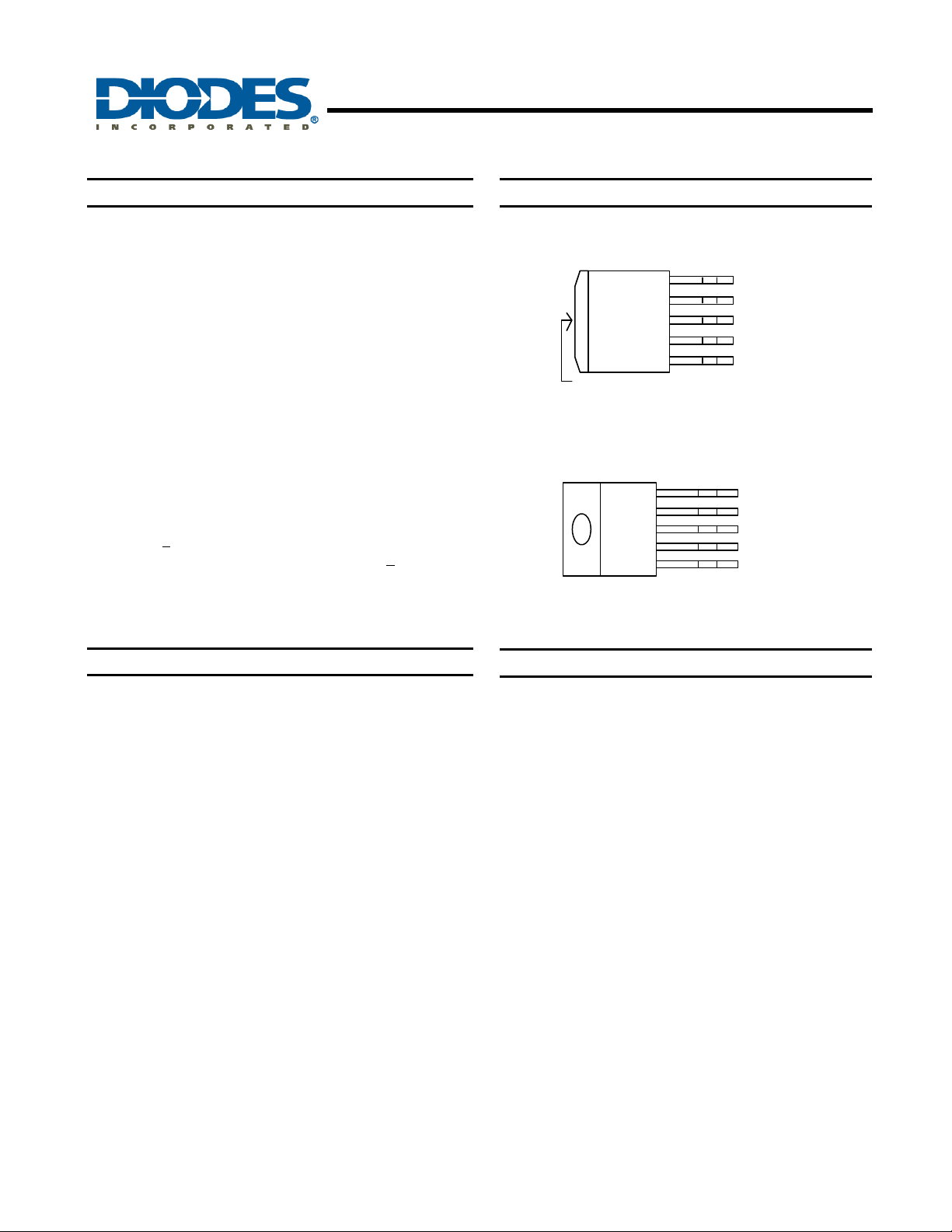
Pin Assignments
( Top View )
Metal Tab GND
TO263-5L
( Top View )
TO220-5L/TO220-5L(R)
5 SD
4 FB
3 Gnd
2 Output
1 V
IN
5 SD
4 FB
3 Gnd
2 Output
1 V
IN
Features
Applications
• Output Voltage: 3.3V, 5V, 12V and Adjustable Output
Version
• Adjustable Version Output Voltage Range, 1.23V to
18V+4%
• 150KHz +15% Fixed Switching Frequency
• Voltage Mode Non-Synchronous PWM Control
• Thermal-Shutdown and Current-Limit Protection
• ON/OFF Shutdown Control Input
• Operating Voltage can be up to 22V
• Output Load Current: 3A
• Lead Free packages: TO263-5L and TO220-5L(R)
• TO263-5L and TO220-5L(R): Available in “Green”
Molding Compound (No Br, Sb)
• Low Power standby mode
• Built-in Switching Transistor On Chip
• Lead Free Finish/RoHS Compliant (Note 1)
Notes: 1. EU Directive 2002/95/EC (RoHS). All applicable RoHS exemptions applied. Please visit our website at
http://www.diodes.com/products/lead_free.html
.
• Simple High-Efficiency Step-Down Regulator
• On-Card Switching Regulators
• Positive to Negative Converter
AP1506
Document number: DS31015 Rev. 7 - 2
1 of 14
www.diodes.com
June 2010
© Diodes Incorporated
Page 2
×
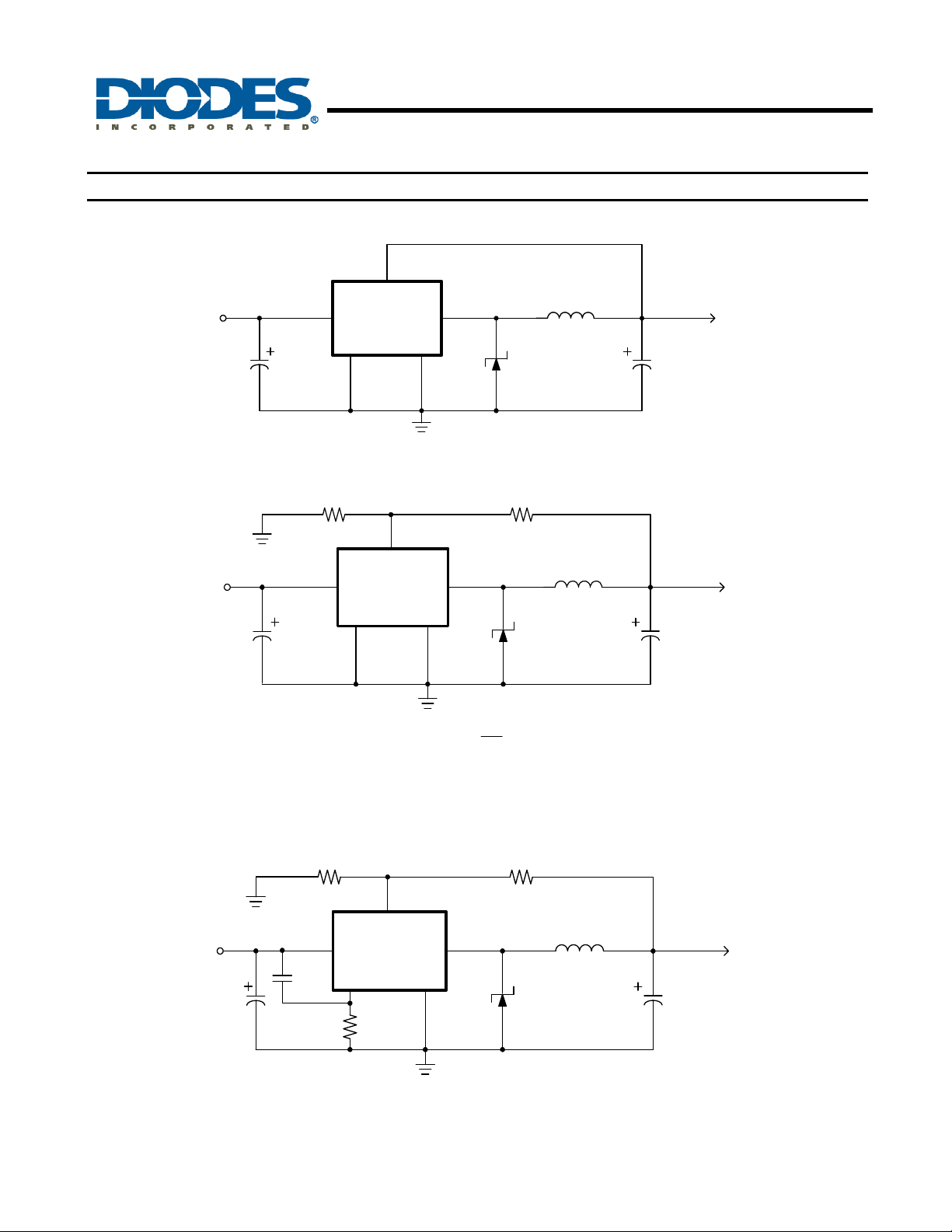
Typical Application Circuit
(1) Fixed Type Circuit
AP1506
150KHz, 3A PWM BUCK DC/DC CONVERTER
12V
DC Input
C
IN
Capacitor
(2) Adjustable Type Circuit
12V
DC Input
C
IN
Capacitor
(3) Delay Start Circuit
FB
4
AP1506
1
V
IN
R2
V
IN
-33
5
SD
12
AP1506
SD
V
out
V
FB
2
3
GND
FB
4
35
= V
FB
= 1.23V
GND
R2 = 1K ~ 3K
R2
Output
Output
(1 +
Schottky Diode
R1
Schottky Diode
R1
)
R2
R1
33
Inductor
D1*
D1*
L1
uH
L1
47uH
3.3V/3A
Output Load
Co
Capacitor
5V/ 3A
Output Load
Co
Capacitor
FB
12V
DC Input
C
IN
Capacitor
V
C
DELAY
0.1uF
4
Output
AP1506
1
IN
5
SD
R
DELAY
2
3
GND
Schottky Diode
L1
47uH
D1*
5V / 3A
Output Load
Co
Capacitor
10K
Notes: 2. For up to 2A = DFLS230L (Vf = 0.42V)
For up to 3A = B340LA, B340LB (V
= 0.45V)
f
AP1506
Document number: DS31015 Rev. 7 - 2
2 of 14
www.diodes.com
June 2010
© Diodes Incorporated
Page 3
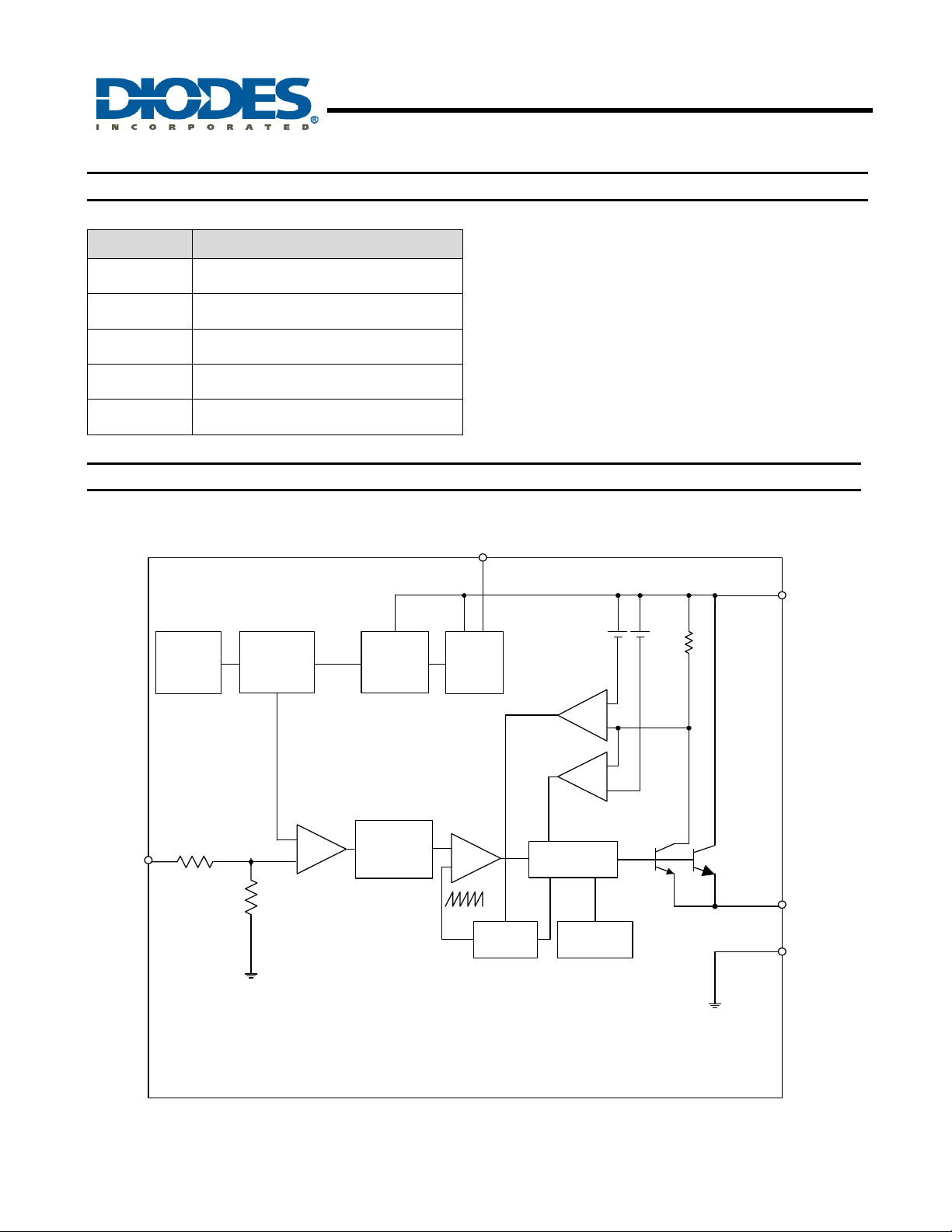
Pin Descriptions
Pin Name Description
VIN Operating Voltage Input
Output Switching Output
GND Ground
FB Output Voltage Feedback Control
SD ON/OFF Shutdown
Functional Block Diagram
AP1506
150KHz, 3A PWM BUCK DC/DC CONVERTER
SD
FB
Current
Source
bias
1.235V
Reference
+
Amp
-
2.5V
Regulator
Frequecy
compen-
sation
Start
up
-
Comp
+
150KHz
OSC.
200mV
Comp
Comp
Pre-driver
Thermal
Shutdown
V
IN
220mV
+
-
-
+
3A
Switch
Output
GND
AP1506
Document number: DS31015 Rev. 7 - 2
3 of 14
www.diodes.com
June 2010
© Diodes Incorporated
Page 4
AP1506
150KHz, 3A PWM BUCK DC/DC CONVERTER
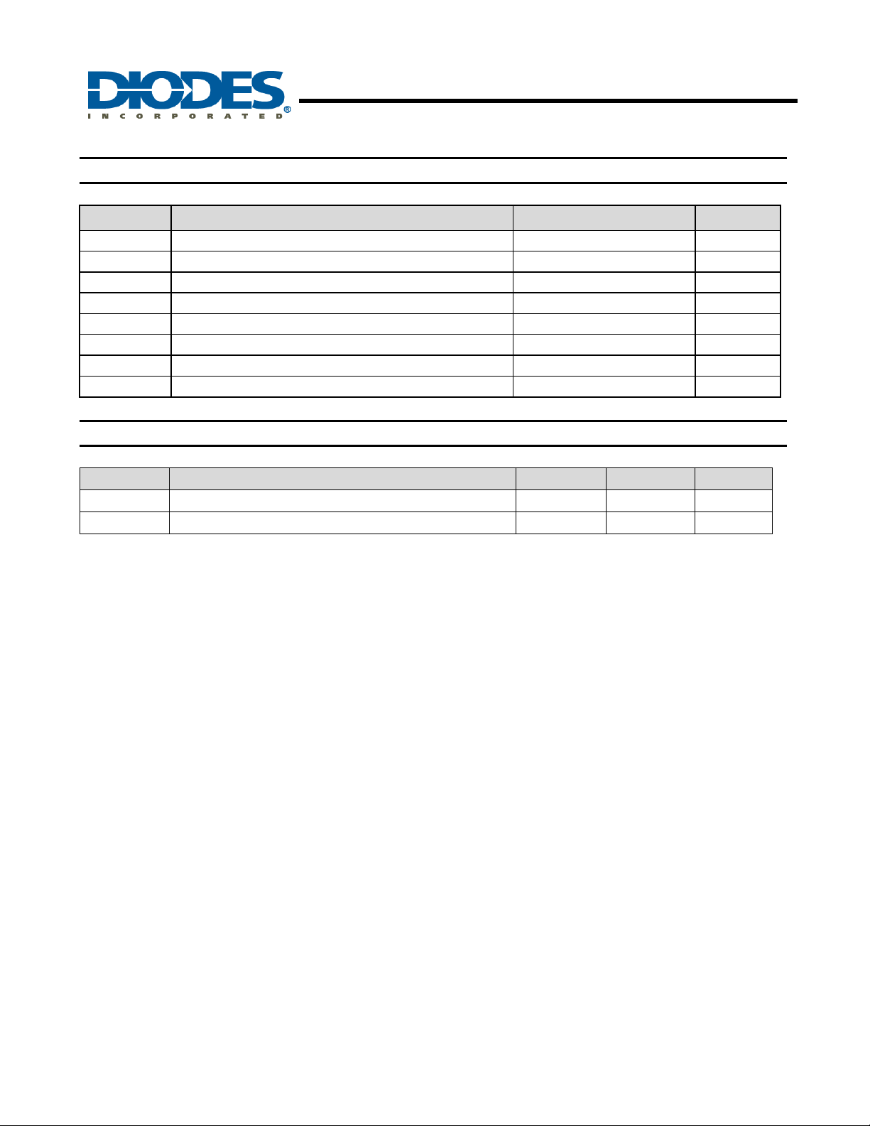
Absolute Maximum Ratings
Symbol Parameter Rating Unit
ESD MM Machine Model ESD Protection 400 V
VCC Supply Voltage +24 V
VSD ON/OFF Pin Input Voltage -0.3 to +18 V
VFB Feedback Pin Voltage -0.3 to +18 V
V
Output Voltage to Ground -1 V
OUT
PD Power Dissipation Internally Limited W
TST Storage Temperature -65 to +150
TOP Operating Junction Temperature -40 to +125
Recommended Operating Conditions
Symbol Parameter Min Max Unit
VOP Operating Voltage 4.5 22 V
TA Operating Ambient Temperature -20 85
o
C
o
C
o
C
AP1506
Document number: DS31015 Rev. 7 - 2
4 of 14
www.diodes.com
June 2010
© Diodes Incorporated
Page 5
AP1506
150KHz, 3A PWM BUCK DC/DC CONVERTER
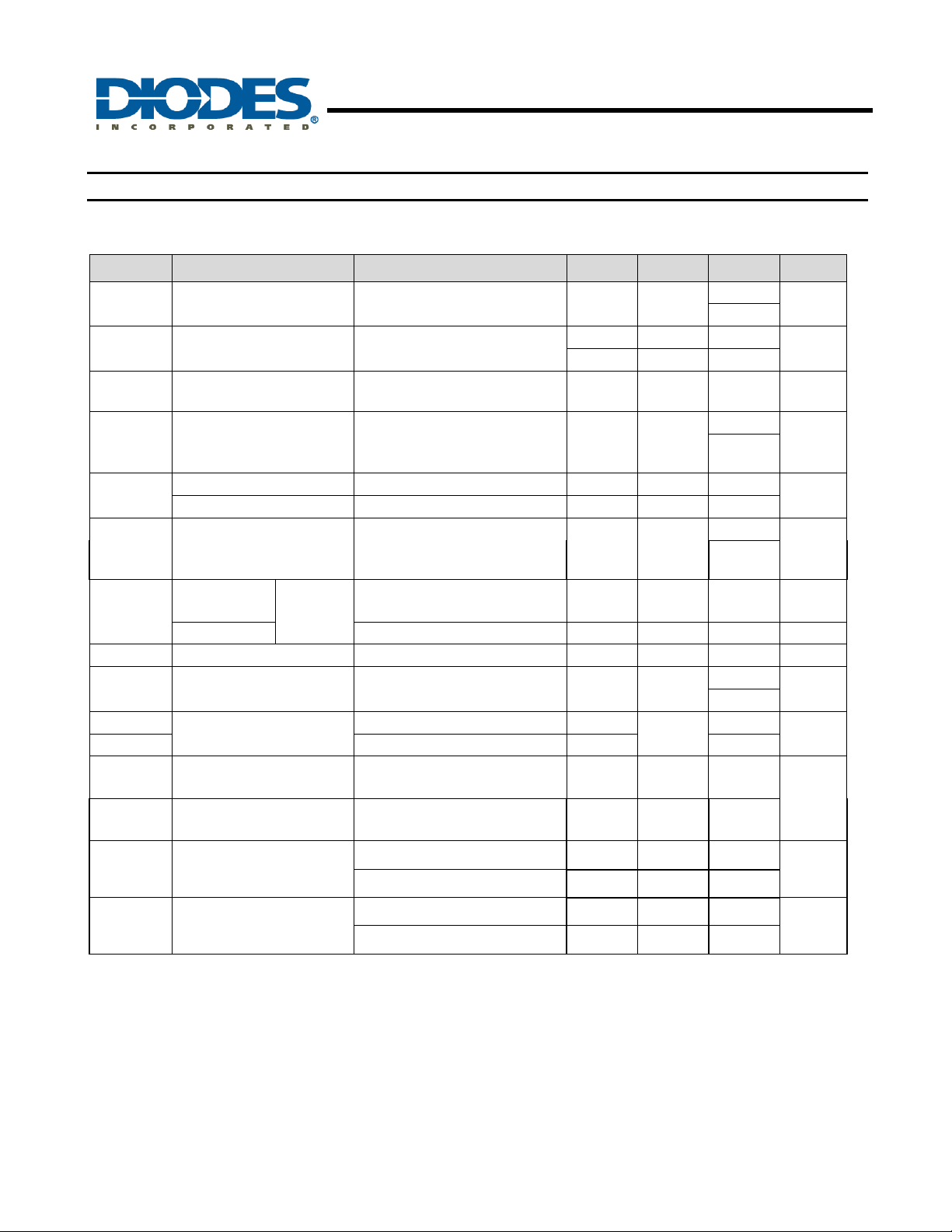
Electrical Characteristics (All Output Voltage Versions)
Unless otherwise specified, V
Specifications with boldface type are for full operating temperature range, the other type are for T
= 12V for 3.3V, 5V, adjustable version and V
IN
Symbol Parameter Conditions Min Typ. Max Unit
V
= 1.3V
IFB Feedback Bias Current
F
Oscillator Frequency
OSC
F
SCP
V
DC
SAT
Oscillator Frequency of
Short Circuit Protect
Saturation Voltage
Max. Duty Cycle (ON) V
Min. Duty Cycle (OFF) V
FB
(Adjustable version only)
When current limit occurred
and V
I
OUT
< 0.5V, Ta = 25 oC
FB
= 3A
No outside circuit
= 0V force driver on
V
FB
= 0V force driver on - 100 -
FB
= 12V force driver off - 0 -
FB
Peak current
ICL Current Limit
Output
Leakage
Current
IL
Output = 0V
Output = -1V V
IQ Quiescent Current V
I
STBY
VIL
VIH High (regulator OFF) 2.0 -
IH
IL
θ
JA
Standby Quiescent
Current
ON/OFF Pin Logic Input
Threshold Voltage
ON/OFF Pin Logic
Input Current
ON/OFF Pin Input
Current
Thermal Resistance
Junction to Ambient
No outside circuit
= 0 force driver on
V
FB
No outside circuit
= 12 force driver off
V
FB
= 22V - -5 - mA
IN
= 12 force driver off - 5 10 mA
FB
ON/OFF pin = 5V
= 22V
V
IN
Low (regulator ON) -
V
= 2.5V (OFF) - - -0.01
LOGIC
V
= 0.5V (ON) - -0.1 -1
LOGIC
TO263-5L (Note 3) 37 TO220-5L(R) (Note 3) 31 -
= 18V for the 12V version. I
IN
= 25ºC.
J
- -10
LOAD
-50
-100
= 0.5A
127 150 173
110
-
173
10 30 50 KHz
1.6
- 1.4
1.7
5.5
3.6 4.5
6.5
- - -200
- 70
1.3
150
200
0.6
nA
KHz
V
%
A
µA
µA
V
µA
o
C/W
θ
JC
Notes: 3. Test condition: Device mounted with copper area of approximately 3 in2, no air flow.
Thermal Resistance
Junction to Case
AP1506
Document number: DS31015 Rev. 7 - 2
TO263-5L (Note 3) 6 TO220-5L(R) (Note 3) 5 -
5 of 14
www.diodes.com
o
C/W
June 2010
© Diodes Incorporated
Page 6
150KHz, 3A PWM BUCK DC/DC CONVERTER
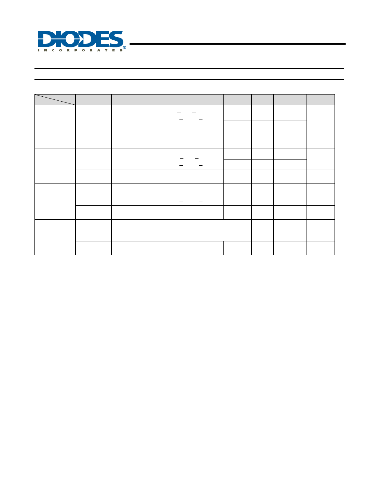
Electrical Characteristics (Continued)
Specifications with boldface type are for full operating temperature range, the other type are for TJ = 25ºC.
AP1506-ADJ
Symbol Parameter Conditions V
VIN < 22V
V
FB
Output
Feedback
5V <
I
0.2A <
V
OUT
LOAD
programmed for
< 3A
1.193 1.23 1.267
3V
η
Efficiency V
= 12V, I
IN
= 3A - 74 - %
LOAD
Typ. V
Min
1.18
Unit
Max
-
1.28
AP1506
V
AP1506-3.3V
AP1506-5V
AP1506-12V
V
OUT
η
V
OUT
η
V
OUT
η
Output
Voltage
Efficiency V
Output
Voltage
Efficiency V
Output
Voltage
Efficiency V
5.5V <
0.2A <
= 12V, I
IN
8V <
0.2A <
= 12V, I
IN
15V <
0.2A <
= 16V, I
IN
VIN < 22V
I
< 3A
LOAD
= 3A - 75 - %
LOAD
VIN < 22V
I
< 3A
LOAD
= 3A - 80 - %
LOAD
VIN < 22V
I
< 3A
LOAD
= 3A - 89 - %
LOAD
3.168 3.3 3.432
3.135
-
3.465
4.8 5 5.2
4.75
-
5.25
11.52 12 12.48
11.4
-
12.6
V
V
V
AP1506
Document number: DS31015 Rev. 7 - 2
6 of 14
www.diodes.com
June 2010
© Diodes Incorporated
Page 7

AP1506
150KHz, 3A PWM BUCK DC/DC CONVERTER
Functional Description
Pin Functions
+V
IN
This is the positive input supply for the IC switching regulator. A suitable input bypass capacitor must be
presented at this pin to minimize voltage transients and to supply the switching currents needed by the regulator.
Ground
Circuit ground.
Output
Internal switch. The voltage at this pin switches between (+V
of approximately V
/ VIN. To minimize coupling to sensitive circuitry, the PC board copper area connected to
OUT
this pin should be kept to a minimum.
Feedback (FB)
Senses the regulated output voltage to complete the feedback loop.
ON/OFF (SD)
Allows the switching regulator circuit to be shutdown using logic level signals thus dropping the total input supply
current to approximately 150uA. Pulling this pin below a threshold voltage of approximately 1.3V turns the
regulator on, and pulling this pin above 1.3V (up to a maximum of 18V) shuts the regulator down. If this shutdown
feature is not needed, the ON / OFF pin can be wired to the ground pin.
Thermal Considerations
The AP1506 is available in two packages: a 5-pin TO220 and a 5-pin surface mount TO263.
The TO220 package needs a heat sink under most conditions. The size of the heat sink depends on the input
voltage, the output voltage, the load current and the ambient temperature. The AP1506 junction temperature rises
above ambient temperature for a 3A load and different input and output voltages. The data for these curves was
taken with the AP1506 (TO220 package) operating as a buck-switching regulator in an ambient temperature of
o
25
C (still air). These temperature rise numbers are all approximate and there are many factors that can affect
these temperatures. Higher ambient temperatures require more heat sinking.
The TO263 surface mount package tab was designed to be soldering to the copper on a printed circuit board. The
copper and the board are the heat sink for this package and the other heat producing components, such as the
catch diode and inductor. The PC board copper area that the package is soldered to should be at least 0.8 in
and ideally should have 2 or more square inches of 2 oz. Additional copper area improves the thermal
characteristics, but with copper areas greater than approximately 6 in
dissipation are realized. If further thermal improvements are needed, double sided, multi-layer PC board with large
copper areas and/or airflow will be recommended.
AP1506
Document number: DS31015 Rev. 7 - 2
7 of 14
www.diodes.com
IN
– V
) and approximately – 0.5V, with a duty cycle
SAT
2
, only small improvements in heat
June 2010
© Diodes Incorporated
2
,
Page 8

AP1506
150KHz, 3A PWM BUCK DC/DC CONVERTER
Functional Description (Continued)
The AP1506 (TO263 package) junction temperature rises above ambient temperature with a 2A load for various
input and output voltages. This data was taken with the circuit operating as a buck-switching regulator with all
components mounted on a PC board to simulate the junction temperature under actual operating conditions. This
curve can be used for a quick check for the approximate junction temperature for various conditions, but be aware
that there are many factors that can affect the junction temperature. When load currents higher than 3A are used,
double sided or multi-layer PC boards with large copper areas and/or airflow might be needed, especially for high
ambient temperatures and high output voltages.
For the best thermal performance, wide copper traces and generous amounts of printed circuit board copper
should be used in the board layout (Once exception to this is the output (switch) pin, which should not have large
areas of copper). Large areas of copper provide the best transfer of heat (lower thermal resistance) to the
surrounding air, and moving air lowers the thermal resistance even further.
Package thermal resistance and junction temperature rise numbers are all approximate, and there are many
factors that will affect these numbers. Some of these factors include board size, shape, thickness, position,
location, and even board temperature. Other factors are: trace width, total printed circuit copper area, copper
thickness, single or double-sided, multi-layer board and the amount of solder on the board. The effectiveness of
the PC board to dissipate heat also depends on the size, quantity and spacing of other components on the board,
as well as whether the surrounding air is still or moving. Furthermore, some of these components such as the
catch diode will add heat to the PC board and the heat can vary as the input voltage changes. For the inductor,
depending on the physical size, type of core material and the DC resistance, it could either act as a heat sink
taking heat away from the board, or it could add heat to the board.
AP1506
Document number: DS31015 Rev. 7 - 2
8 of 14
www.diodes.com
June 2010
© Diodes Incorporated
Page 9
f
f
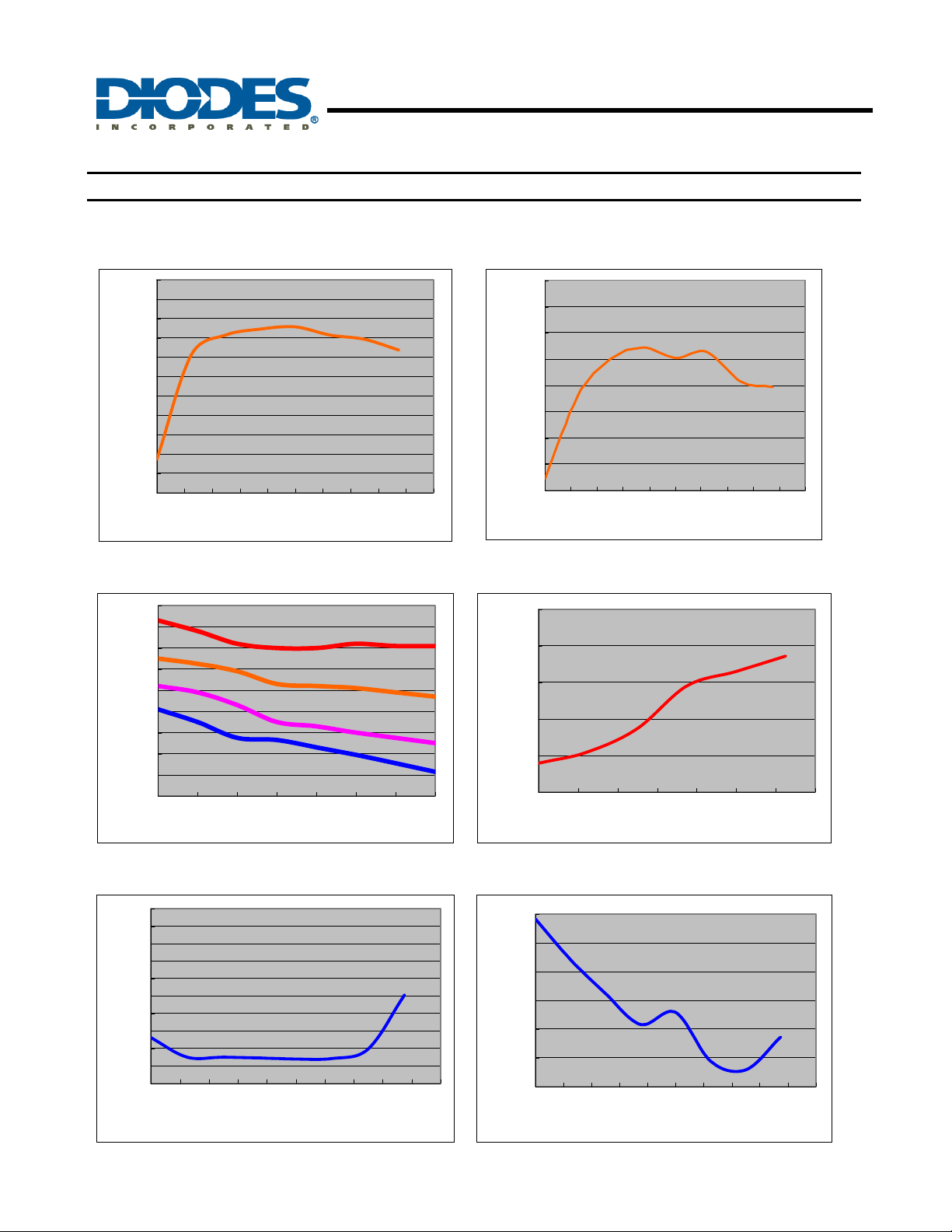
Typical Performance Characteristics
AP1506 Efficiency vs. Temperature
(V
= 12V, V
IN
83
82
81
80
79
78
77
76
75
Efficiency (%)
74
73
72
-50 -30 -10 10 30 50 70 90 110 130 150
Temperature (TA)
= 5V, Io = 3A)
OUT
AP1506
150KHz, 3A PWM BUCK DC/DC CONVERTER
AP1506 Efficiency vs. Temperature
(V
= 12V, V
IN
78
77
76
75
74
73
72
Efficiency (%)
71
70
-50 -30 -10 10 30 50 70 90 110 130 150
Temperatur e ( TA) (oC)
= 3.3V, Io = 3A)
OUT
AP1506 Saturation Voltage vs. Temperature
(Vcc = 12V, V
1.6
1.5
1.4
1.3
1.2
1.1
1
0.9
0.8
Saturation Voltage (V)
0.7
-50 -25 0 25 50 75 100 125
Temperature (TA) (oC)
= 0V, VSD = 0)
FB
2A
1A
0.5A
3A
AP1506 Supply Current vs. Temperature
(Vcc = 12V, No Load, V
15
14
13
12
11
10
9
8
7
6
Supply Current (mA)
5
-50 -30 -10 10 30 50 70 90 110 130 150
Switch ON
Temperature (TA) (oC)
= 0V (Switch ON), V
on/of
AP1506 Switch Current Limit vs. Temperature
(Vcc = 12V, V
5.5
5
4.5
4
3.5
Switch Current Limit (A)
3
-50-30-101030507090
60
55
50
45
40
35
Supply Current (uA)
30
-50 -30 -10 10 30 50 70 90 110 130 150
Temperature (TA) (oC)
= 5V (Switch OFF))
on/of
Switch OFF
Temperature (TA) (oC)
= 0V)
FB
AP1506
Document number: DS31015 Rev. 7 - 2
9 of 14
www.diodes.com
June 2010
© Diodes Incorporated
Page 10
150KHz, 3A PWM BUCK DC/DC CONVERTER
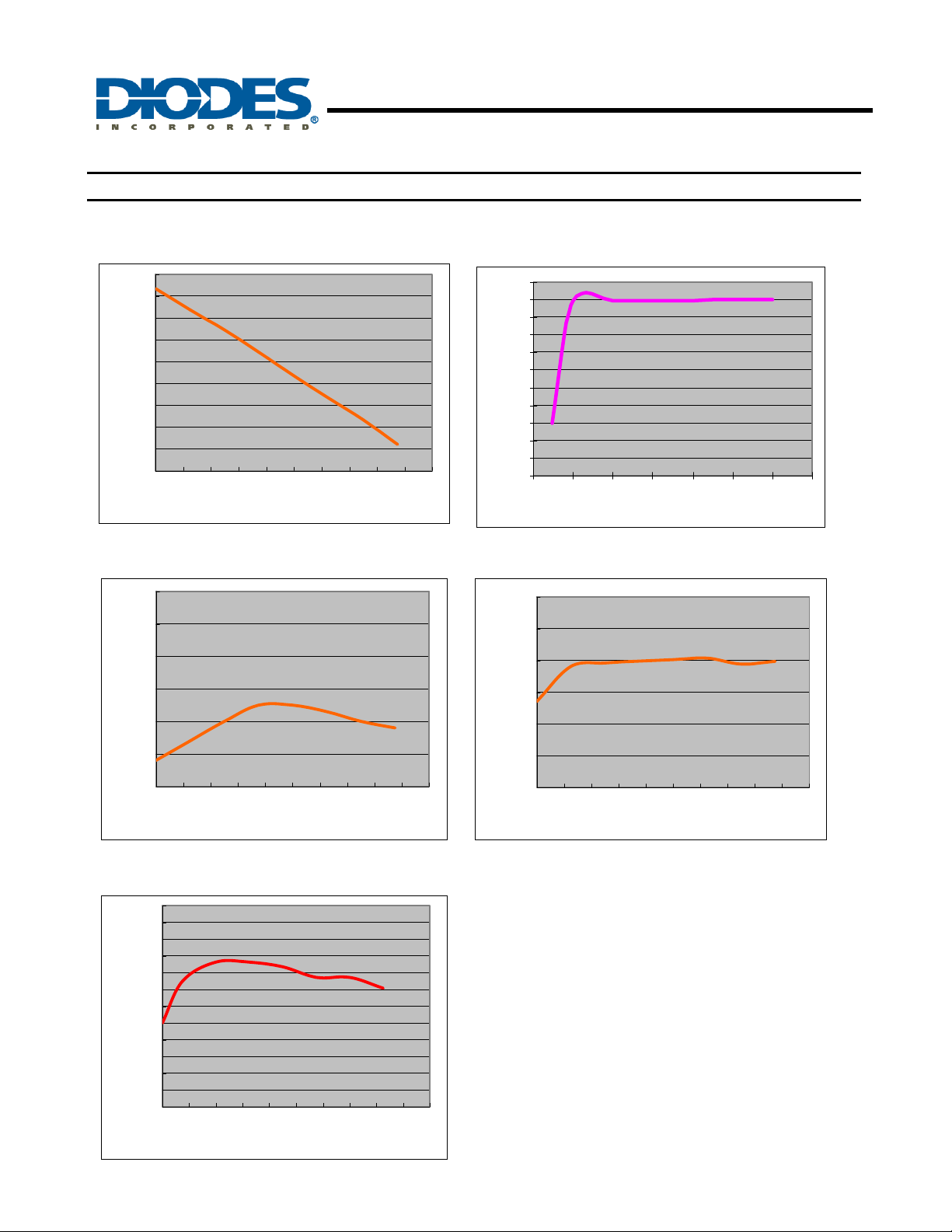
Typical Performance Characteristics (Continued)
AP1506 Threshold Voltage vs. Temperature
(Vcc = 12V, Io = 100mA)
1.7
1.6
1.5
1.4
1.3
1.2
1.1
1
0.9
Threshold Voltage (V)
0.8
-50 -30 -10 10 30 50 70 90 110 130 150
Temperature (TA) (oC)
AP1506 Frequency vs. Temperature
(Vcc = 12V, Ic = 500mA, V
170
OUT
= 5V)
AP1506 ON/OFF Current vs. ON/OFF Voltage
AP1506 Feedback Current vs. Temperature
AP1506
(V
= 12V)
IN
10
0
-10
-20
-30
-40
-50
-60
-70
-80
ON/OFF Current (nA)
-90
-100
036912151821
ON/OFF Voltage (V)
(Vcc = 12V, V
10
OUT
= 5V, V
= 1.3V)
FB
165
160
155
150
Frequency (KHz)
145
140
-50 -30 -10 10 30 50 70 90 110 130 150
Temperature (TA) (oC)
AP1506 Output Voltage vs. Temperature
(V
= 12V, Io = 3A)
IN
3.5
3.45
3.4
3.35
3.3
3.25
(V)
3.2
out
3.15
V
3.1
3.05
3
2.95
2.9
-40 -20 0 20 40 60 80 100 120 140 160
Temperature (TA) (oC)
0
-10
-20
-30
-40
Feedback Current (nA)
-50
-50 -30 -10 10 30 50 70 90 110 130 150
Temperature (TA) (oC)
AP1506
Document number: DS31015 Rev. 7 - 2
10 of 14
www.diodes.com
June 2010
© Diodes Incorporated
Page 11
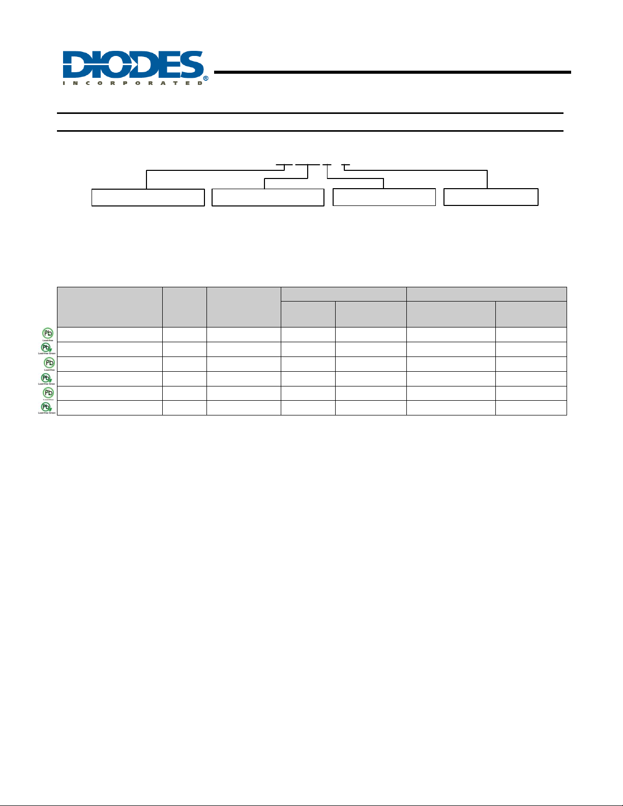
Ordering Information
AP1506
150KHz, 3A PWM BUCK DC/DC CONVERTER
Output version
Blank : Adjustable
33 : 3.3V
50 : 5.0V
AP1506 - XX
Package
K5 : TO263-5L
T5 : TO220-5L
T5R : TO220-5L(R)
XXX X - X
Lead Free
L : Lead Free
G : Green
Packing
U : Tube
13 : Tape & Reel
12 : 12V
Device
AP1506-XXK5L-13 K5 TO263-5L NA NA 800/Tape & Reel -13
AP1506-XXK5G-13 K5 TO263-5L NA NA 800/Tape & Reel -13
AP1506-XXT5L-U T5 TO220-5L 50 -U NA NA
AP1506-XXT5G-U T5 TO220-5L 50 -U NA NA
AP1506-XXT5RL-U T5R TO220-5L(R) 50 -U NA NA
AP1506-XXT5RG-U T5R TO220-5L(R) 50 -U NA NA
Notes: 4. Pad layout as shown on Diodes Inc. suggested pad layout document AP02001, which can be found on our website at
http://www.diodes.com/datasheets/ap02001.pdf.
Package
Code
Packaging
(Note 4)
Quantity
Tube/Bulk 13” Tape and Reel
Part Number
Suffix
Quantity
Part Number
Suffix
AP1506
Document number: DS31015 Rev. 7 - 2
11 of 14
www.diodes.com
June 2010
© Diodes Incorporated
Page 12
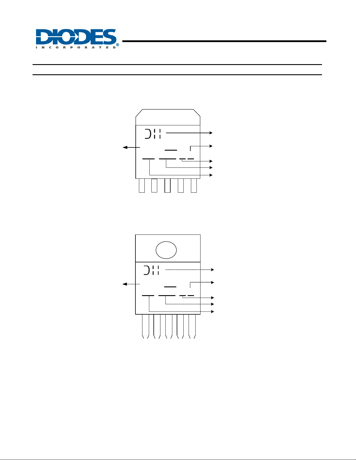
Marking Information
(1) TO263-5L
Output Type:
1506 : ADJ
1506-33 : 3.3V
1506-50 : 5.0V
1506-12 : 12V
(2) TO220-5L(R)
( Top view )
1506-XX
YY WW
( Top view )
AP1506
150KHz, 3A PWM BUCK DC/DC CONVERTER
Logo
L : Lead Free
X
X
G : Green
ID code
Xth week: 01~52
Year:
"07" = 2007
"08" = 2008
~
Logo
Output Type:
1506 : ADJ
1506-33 : 3.3V
1506-XX
YY WW X X
1506-50 : 5.0V
1506-12 : 12V
L : Lead Free
G : Green
ID code
Xth week: 01~52
Year:
"07" = 2007
"08" = 2008
~
AP1506
Document number: DS31015 Rev. 7 - 2
12 of 14
www.diodes.com
June 2010
© Diodes Incorporated
Page 13
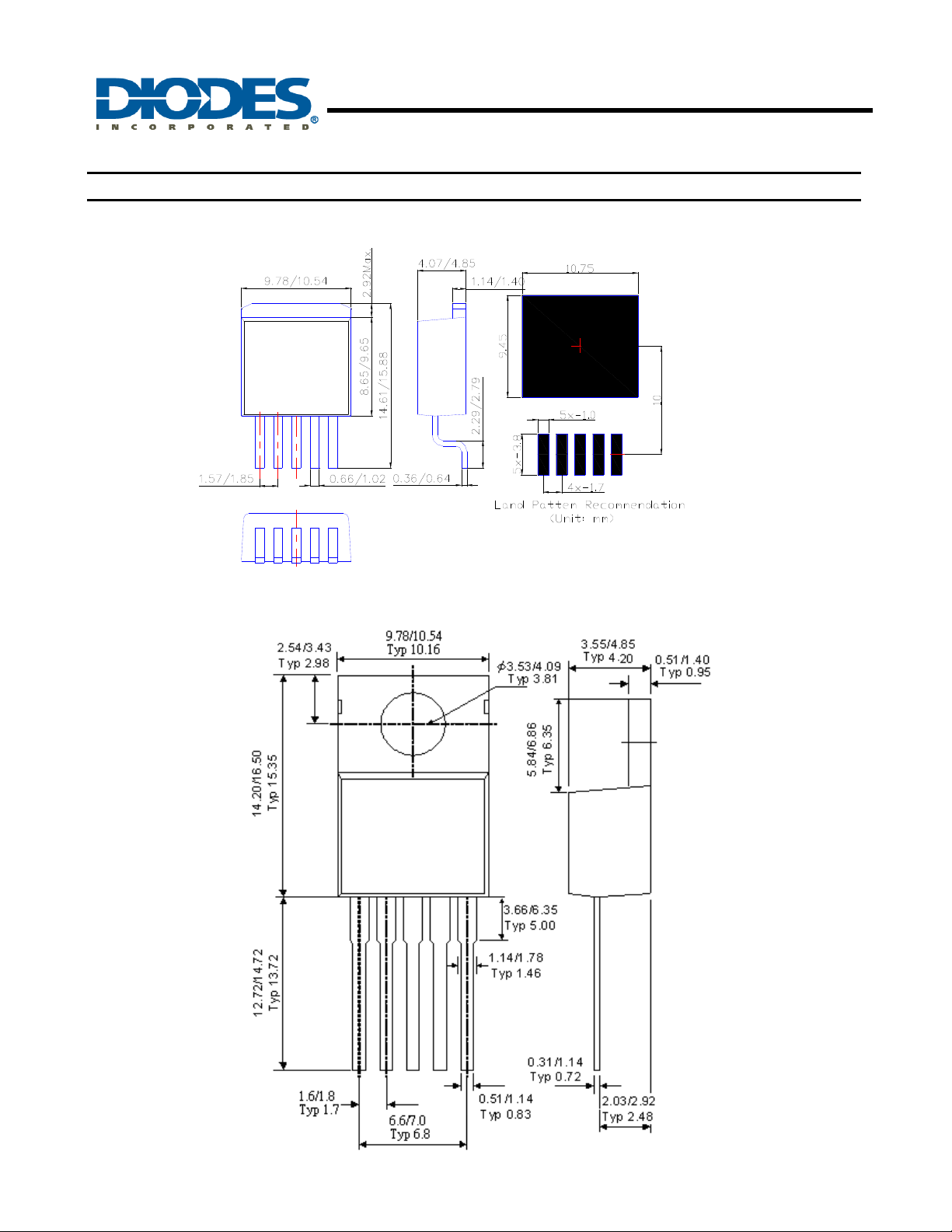
150KHz, 3A PWM BUCK DC/DC CONVERTER
Package Outline Dimensions (All Dimensions in mm)
(1) Package Type: TO263-5L
AP1506
(2) Package Type: TO220-5L
AP1506
Document number: DS31015 Rev. 7 - 2
13 of 14
www.diodes.com
June 2010
© Diodes Incorporated
Page 14

AP1506
150KHz, 3A PWM BUCK DC/DC CONVERTER
IMPORTANT NOTICE
DIODES INCORPORATED MAKES NO WARRANTY OF ANY KIND, EXPRESS OR IMPLIED, WITH REGARDS TO THIS
DOCUMENT, INCLUDING, BUT NOT LIMITED TO, THE IMPLIED WARRANTIES OF MERCHANTABILITY AND FITNESS FOR A
PARTICULAR PURPOSE (AND THEIR EQUIVALENTS UNDER THE LAWS OF ANY JURISDICTION).
Diodes Incorporated and its subsidiaries reserve the right to make modifications, enhancements, improvements, corrections or other
changes without further notice to this document and any product described herein. Diodes Incorporated does not assume any liability
arising out of the application or use of this document or any product described herein; neither does Diodes In corporated convey any
license under its patent or trademark rights, nor the rights of others. Any Customer or user of this documen t or products described
herein in such applications shall assume all risks of such use and will agree to hold Diodes Incorporated and all the companies
whose products are represented on Diodes Incorporated website, harmless against all damages.
Diodes Incorporated does not warrant or accept any liability whatsoever in respect of any products purchased through unauthorized
sales channel.
Should Customers purchase or use Diodes Incorporated products for any unintended or unauthorized application, Customers shall
indemnify and hold Diodes Incorporated and its representatives harmless against all claims, damages, expenses, and attorney fees
arising out of, directly or indirectly, any claim of personal injury or death associated with such unintended or unauthorized application.
Products described herein may be covered by one or more United States, international or foreign p atents pending. Product names
and markings noted herein may also be covered by one or more United States, international or foreign trademarks.
LIFE SUPPORT
Diodes Incorporated products are specifically not authorized for use as critical components in life support devices or systems without
the express written approval of the Chief Executive Officer of Diodes Incorporated. As used herein:
A. Life support devices or systems are devices or systems which:
1. are intended to implant into the body, or
2. support or sustain life and whose failure to perform when properly used in accordance with instructions for use provided
in the labeling can be reasonably expected to result in significant injury to the user.
B. A critical component is any component in a life support device or system whose failure to perform can b e reasonably expected
to cause the failure of the life support device or to affect its safety or effectiveness.
Customers represent that they have all necessary expertise in the safety and regulatory ramifications of their life support dev ices or
systems, and acknowledge and agree that they are solely responsible for all legal, regulatory and safety-related requirements
concerning their products and any use of Diodes Incorporated products in such safety-critical, life support devices or systems,
notwithstanding any devices- or systems-related information or support that may be provided by Diodes Incorporated. Further,
Customers must fully indemnify Diodes Incorporated and its representatives against any damages arising out of the use of Diodes
Incorporated products in such safety-critical, life support devices or systems.
Copyright © 2010, Diodes Incorporated
www.diodes.com
AP1506
Document number: DS31015 Rev. 7 - 2
14 of 14
www.diodes.com
June 2010
© Diodes Incorporated
 Loading...