

Page 1
AP1086
1.5A LOW DROPOUT POSITIVE ADJUSTABLE OR
FIXED-MODE REGULATOR
Description
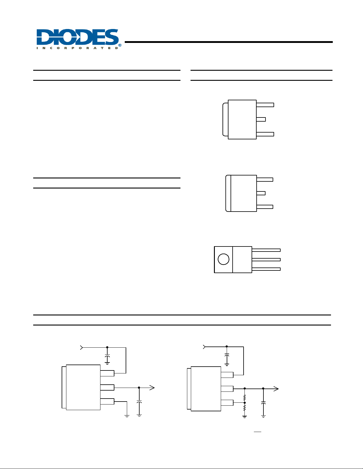
AP1086 is a low dropout positive adjustable or fixed-mode
regulator with 1.5A output current capability. The product is
Pin Assignments
(Top View)
3
specifically designed to provide well-regulated su pply for low
voltage IC applications such as high-speed bus termination
2
and low current 3.3V logic supply. AP1086 is also well suited
for other applications such as VGA cards. AP1086 is
guaranteed to have lower than 1.4V dropout at full load
current making it ideal to provide well-regulated outputs of
1.25V to 5.0V with 4.7 to 12V input supply by different output
voltage.
Features
• 3-Terminal Adjustable or Fixed 1.5V, 1.8V, 2.5V,3.3V,
5.0V
• 1.4V Maximum Dropout at Full Load Current
• Fast Transient Response
• Built-in Thermal Shutdown
• Output Current Limiting
• Lead Free Packages: TO252-3L, TO263-3L, TO220-3L
• TO252-3L, TO263-3L, and TO220-3L: Available in
“Green” Molding Compound (No Br, Sb)
• Lead Free Finish/ RoHS Compliant (Note 1)
1
Tab is V
OUT
TO252-3L
(Top View)
3
2
1
Tab is V
OUT
TO263-3L
(Top View)
3
2
1
Tab is V
OUT
TO220-3L
Notes: 1. EU Directive 2002/95/EC (RoHS). All applicable RoHS exemptions applied. Please visit our website at
http://www.diodes.com/products/lead_free.html.
V
V
OUT
V
OUT
Adj (GND)
IN
Adj (GND)
V
IN
V
IN
V
OUT
Adj (GND)
Typical Application Circuit
5V to 3.3V Fixed Mode Regulator
5V
C1
100uF
Vin
Vout
GND
Tab is Vout
AP1086
Document number: DS31028 Rev. 6 - 2
C2
100uF
3.3V/1.5A
1 of 10
www.diodes.com
Tab is Vout
Adjustable Regulator
5V
Vout
Note:
Vin
Adj
o
C1
100uF
RE
F
V
OUT=Vref
R1
121
R2
121
(
VV +∗=
1
Ω
Ω
R
2
)
R
1
×
(1+R2/R1)
2.5V/1.5A
C2
100uF
June 2010
© Diodes Incorporated
Page 2
1.5A LOW DROPOUT POSITIVE ADJUSTABLE OR
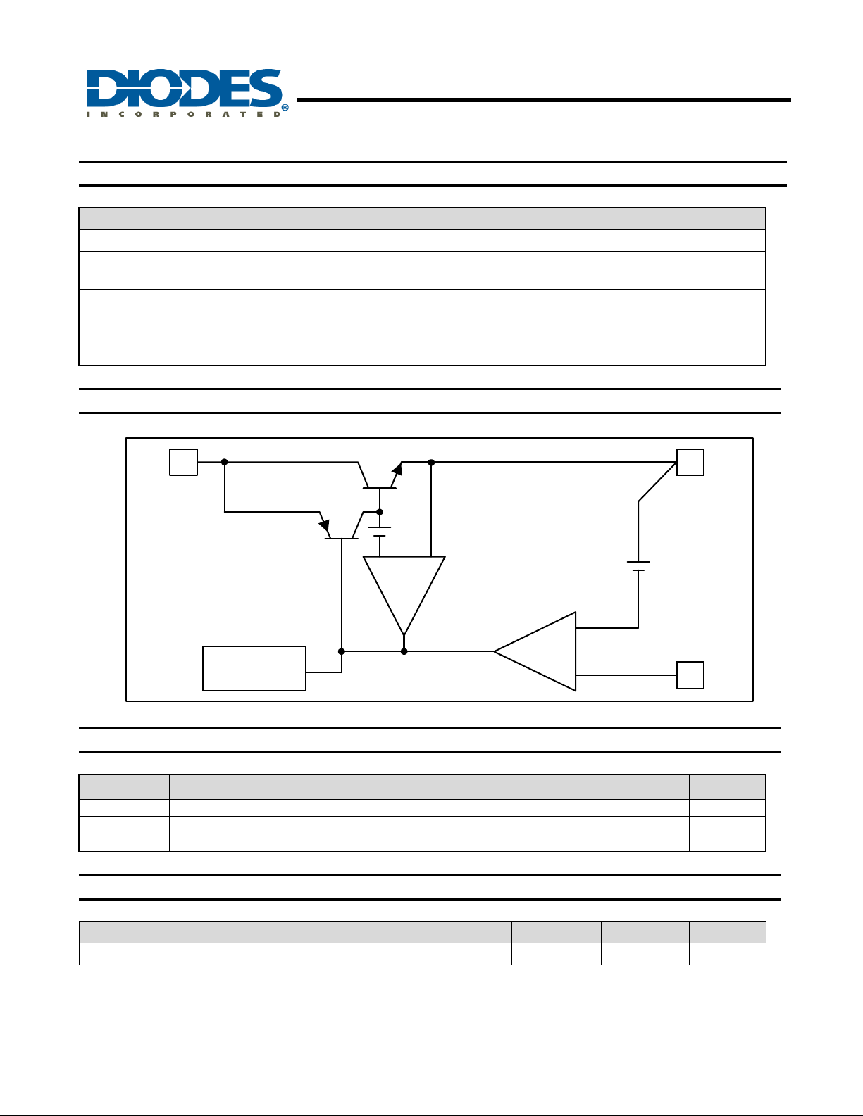
Pin Descriptions
Pin Name I/O Pin # Description
Adj (GND) 1 Adjustable (Ground only for fixed mode)
V
O 2
OUT
VIN I 3
Functional Block Diagram
The output of the regulator. A minimum of 10uF capacitor must be connected
from this pin to ground to insure stability.
The input pin of regulator. Typically a large storage capacitor is connected
from this pin to ground to insure that the input voltage does not sag below the
minimum dropout voltage during the load transient response. This pin must
always be 1.4V higher than V
in order for the device to regulate properly.
OUT
AP1086
FIXED-MODE REGULATOR
3
V
IN
2
+
+
-
1.25V
+
CURRENT
LIMIT
+
Thermal
Shutdown
-
1
Absolute Maximum Ratings
Symbol Parameter Rating Unit
VIN DC Supply Voltage -0.3 to 12 V
TST Storage Temperature -65 to +150
TMJ Maximum Junction Temperature 150
V
Adj
o
o
OUT
C
C
Recommended Operating Conditions
Symbol Parameter Min Max Unit
Top Operating Junction Temperature Range
0 125
AP1086
Document number: DS31028 Rev. 6 - 2
2 of 10
www.diodes.com
© Diodes Incorporated
o
C
June 2010
Page 3
AP1086
1.5A LOW DROPOUT POSITIVE ADJUSTABLE OR
FIXED-MODE REGULATOR
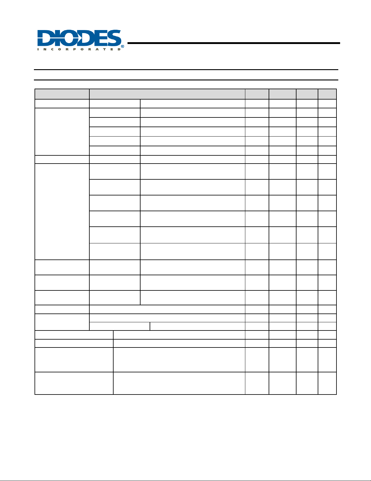
Electrical Characteristics (Under Operating Conditions)
Parameter Conditions
Reference Voltage AP1086-Adj
AP1086-1.5
AP1086-1.8
Output Voltage
AP1086-2.5
AP1086-3.3
AP1086-5.0
Line Regulation AP1086-XXX IO = 10mA, V
AP1086-Adj
AP1086-1.5
AP1086-1.8
Load Regulation
AP1086-2.5
AP1086-3.3
AP1086-5.0
Dropout Voltage
IN-VOUT
)
(V
Current Limit
Minimum Load
Current (Note 4)
Thermal Regulation
Ripple Rejection
RMS Noise (% of V
AP1086-Adj/-2.5/
-3.3/-3.6/-5.0
AP1086-Adj/-2.5/
-3.3/-3.6/-5.0
AP1086-XXX
T
= 25οC, 30ms pulse
A
f = 120Hz,C
OUT
AP1086-XXX V
OUT
)
10Hz ≤ f ≤ 10KHz
T
= 25οC, (VIN-V
A
I
= 10mA, TA = 25οC, 3V≦VIN≦12V
OUT
= 10mA, TA = 25οC, 3.3V≦VIN≦12V
I
OUT
= 10mA, TA = 25οC, 4V≦VIN≦12V
I
OUT
I
= 10mA, TA = 25οC, 4.8V≦VIN≦12V
OUT
I
= 10mA, TA = 25οC, 6.5V≦VIN≦12V
OUT
V
= 3.3V, 0mA<Io<1.5A, TA = 25οC
IN
(Note 2, 3)
V
= 3V, 0mA<Io<1.5A, TA = 25οC
IN
(Note 2, 3)
V
= 3.3V, 0mA<Io<1.5A, TA = 25οC
IN
(Note 2, 3)
V
= 4V, 0mA<Io<1.5A, TA = 25οC
IN
(Note 2, 3)
V
= 5V, 0≦I
IN
T
= 25oC (Note 2, 3)
J
= 8V, 0≦I
V
IN
T
= 25oC (Note 2, 3)
J
I
= 1.5A, ΔV
OUT
(VIN-V
o
0
) = 5V 1. 6 - - A
OUT
C≦TJ≦125oC
= 25uF Tantalum, I
= V
IN
OUT
)= 1.5V,IO = 10mA
OUT
+1.5V<VIN<12V - - 0.2 %
OUT
≦1.5A, TA = 25οC,
OUT
≦1.5A, TA = 25οC,
OUT
= 1%V
OUT
= 1.5A
OUT
OUT
+3V - 60 70 dB
Temperature Stability IO = 10mA - 0.5 - %
θ
Thermal Resistance
JA
Junction-to-Ambient
(No heat sink; No air flow)
θ
Thermal Resistance
JC
Junction-to-Case
Notes: 2. See thermal regulation specifications for changes in output voltage due to heating effects. Line and load regulation are measured at a constant
junction temperature by low duty cycle pulse testing. Load regulation is measured at the output lead = 1/18” from the package.
3. Line and load regulation are guaranteed up to the maximum power dissipation of 15W. Power dissipation is determined by the difference in input and
output and the output current. Guaranteed maximum power dissipation will not be available over the full input/output range.
4. Quiescent current is defined as the minimum output current required in maintaining regulation. At 12V input/output differential the device is
guaranteed to regulate if the output current is greater than 10mA.
TO252-3L
TO263-3L
TO220-3L
TO252-3L: Control Circuitry/Power Transistor
TO263-3L: Control Circuitry/Power Transistor
TO220-3L: Control Circuitry/Power Transistor
Min Typ. Max Unit
1.225 1.250 1.275
1.470 1.500 1.530 V
1.764 1.800 1.836 V
2.450 2.500 2.550 V
3.235 3.300 3.365 V
4.900 5.000 5.100 V
- - 1 %
- 12 15 mV
- 15 18 mV
- 20 25 mV
- 26 33 mV
- 40 50 mV
- 1.3 1.4 V
- 5 10 mA
- 0.008 0.04 %/W
- 0.003 - %
-
-
101
83
86
15
0.65/2.7
0.65/2.7
o
C/W
-
o
C/W
-
AP1086
Document number: DS31028 Rev. 6 - 2
3 of 10
www.diodes.com
June 2010
© Diodes Incorporated
Page 4

AP1086
1.5A LOW DROPOUT POSITIVE ADJUSTABLE OR
FIXED-MODE REGULATOR
Functional Description
Introduction
The AP1086 adjustable or fixed-mode Low Dropout (LDO) regulator is a 3 terminal device which can easily be
programmed by internal mask change to any voltages within the range of 1.25V to V
needs 1.4V differential between V
and V
IN
to maintain output regulation. In addition, the output voltage
OUT
tolerances are also extremely tight and they include the transient response as part of the specification. For
example, Intel VRE specification calls for a total of +/- 100mV including initial tolerance, load regulation and 0 to
1.5A load step.
The AP1086 is specifically designed to meet the fast current transient needs as well as providing an accurate
initial voltage, reducing the overall system cost with the need for fewer output capacitors.
Load Regulation
Since the AP1086 is only a 3 terminal device, it is not possible to provide true remote sensing of the output
voltage at the load. But it can supply good load regulation by internal feedback bypass the external loss such as
adjustable mode.
Stability
The AP1086 requires the use of an output capacitor as part of the frequency compensation in order to make the
regulator stable. For most applications a minimum of 10uF aluminum electrolytic capacitor insures both stability
and good transient response.
-1.4V. The AP1086 only
IN
Thermal Design
The AP1086 incorporates an internal thermal shutdown that protects the device when the junction temperature
exceeds the maximum allowable junction temperature. Although this device can operate with junction
temperatures in the range of 150
o
C, it is recommended that the selected heat sink be chosen such that during
maximum continuous load operation the junction temperature is kept below the temperature.
Layout Consideration
The output capacitors must be located as close to the V
to use a section of a layer of the PC board as a plane to connect the V
terminal of the device as possible. It is recommended
OUT
pin to the output capacitors to prevent
OUT
any high frequency oscillation that may result due to excessive trace inductance.
AP1086
Document number: DS31028 Rev. 6 - 2
4 of 10
www.diodes.com
June 2010
© Diodes Incorporated
Page 5
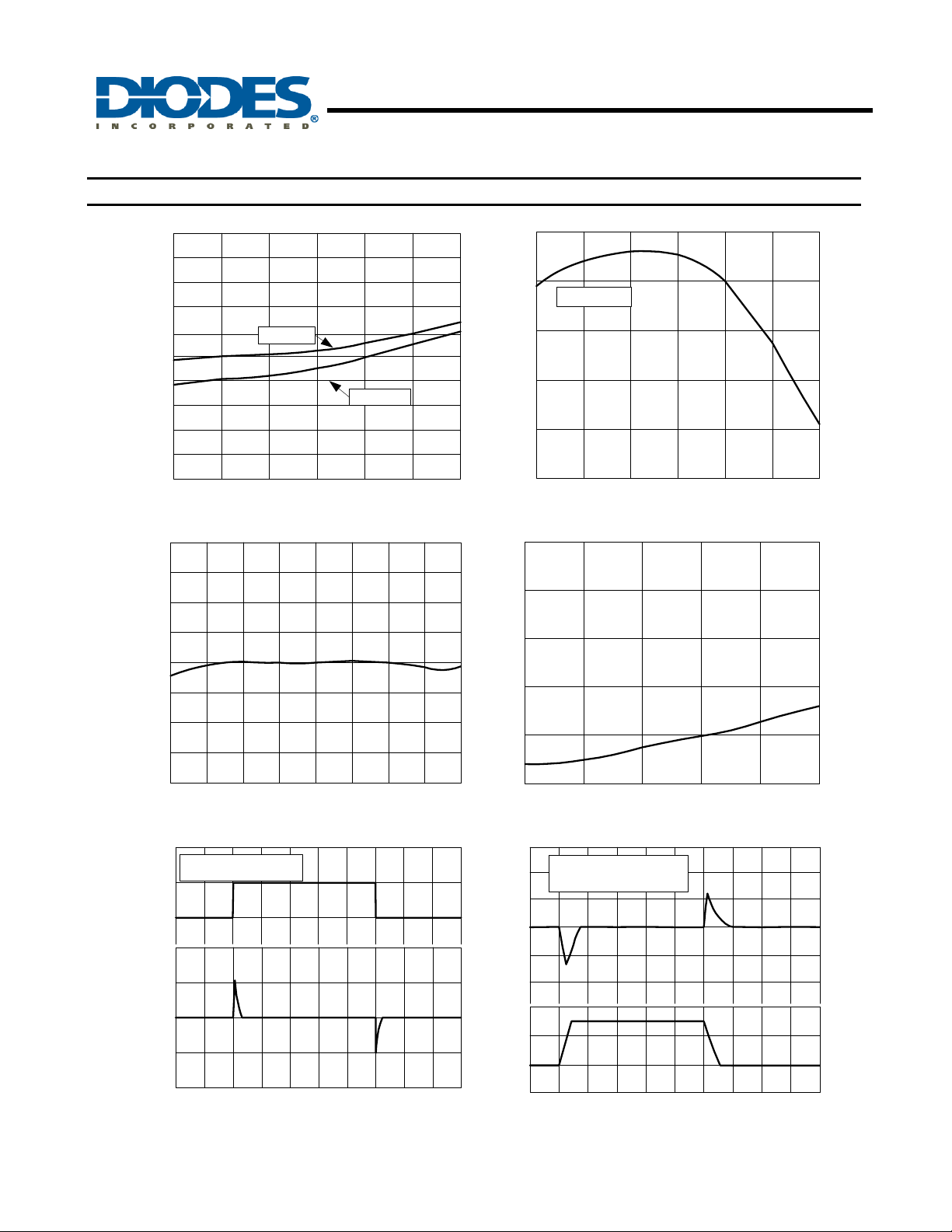
Typical Performance Characteristics
2. 0
1. 8
1. 6
1. 4
1. 2
1. 0
0. 8
0. 6
Dropout Voltage (V)
0. 4
0. 2
0
0.25 0.5 0.75 1.0 1.25 1.5
0
Dropout Voltage vs Output Current
Tj = 25 oC
Tj = 125 oC
Output Current (A)
AP1086
1.5A LOW DROPOUT POSITIVE ADJUSTABLE OR
FIXED-MODE REGULATOR
0.20
0
I load=1.5A
-0.20
-0.40
-0.80
Output Voltage Deviation (%)
- 1
-25 0
Load Regulation vs Temperature
25 50 75 100 125
Temperature (oC)
2
1.5
1
0. 5
0
-0.5
- 1
-1.5
Output Voltage Change (%)
- 2
-50 -25 0 25 50 75 100 125 150
Temperature (oC)
Percent Change in Output Voltage vs Temperature
7.5
Cin=1uF
Cout=10uF Tantalum
6.5
5.5
40
20
1
0.8
0.6
0.4
0.2
Output Voltage Deviation (%)
0
24
30
Cin=1uF
20
Cout=10uF Tantalum
Preload=100mA
10
0
-10
-20
6 8 10 12
Input Voltage (V)
Line Regulation
0
-20
-40
0 20 40 60 80 100 120 140 160 180 200
Output Voltage Deviation (mV) Input Voltage (V)
TIME (us)
Line Transient Response
AP1086
Document number: DS31028 Rev. 6 - 2
Output Voltage Deviation (mV)
2
1
0
-1
010
Load Current (A)
5 of 10
www.diodes.com
20 30 40 50 60 70 80 90 100
TIME (us)
Load Transient Response
© Diodes Incorporated
June 2010
Page 6
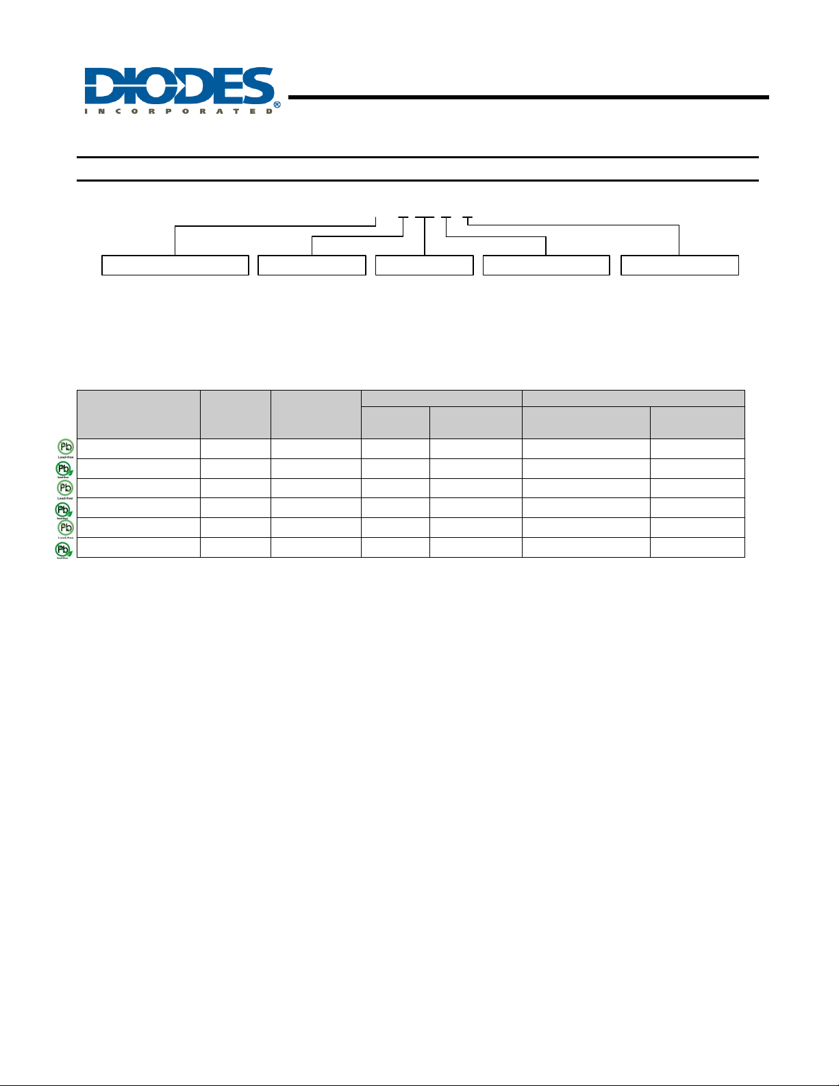
Ordering Information
AP1086
1.5A LOW DROPOUT POSITIVE ADJUSTABLE OR
FIXED-MODE REGULATOR
AP1086 X XX X - X
Low Dropout Regulator Package Vout
D : TO252-3L
K : TO263-3L
T : TO220-3L
Blank = Adj
15 = 1.5V
18 = 1.8V
25 = 2.5V
33 = 3.3V
50 = 5.0V
Lead Free
L : Lead Free
G : Green
Packing
U : Tube
13 : Taping & Reel
Tube 13” Tape and Reel
Part Number
Suffix
Quantity
Part Number
Suffix
Device
Package
Code
Packaging
(Note 5)
Quantity
AP1086DXXL-13 D TO252-3L NA NA 2500/Tape & Reel -13
AP1086DXXG-13 D TO252-3L NA NA 2500/Tape & Reel -13
AP1086KXXL-13 K TO263-3L NA NA 800/Tape & Reel -13
AP1086KXXG-13 K TO263-3L NA NA 800/Tape & Reel -13
AP1086TXXL-U T TO220-3L 50 -U NA NA
AP1086TXXG-U T TO220-3L 50 -U NA NA
Notes: 5. Pad layout as shown on Diodes Inc. suggested pad layout document AP02001, which can be found on our website at
http://www.diodes.com/datasheets/ap02001.pdf.
AP1086
Document number: DS31028 Rev. 6 - 2
6 of 10
www.diodes.com
June 2010
© Diodes Incorporated
Page 7
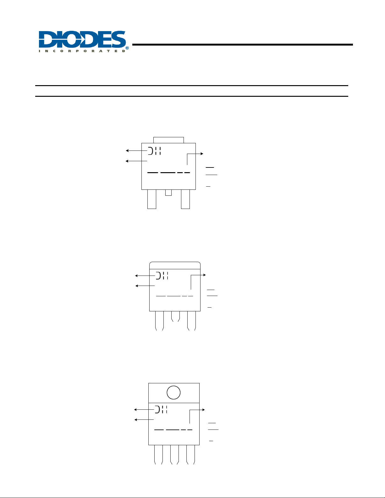
Marking Information
(1) TO252-3L
AP1086
1.5A LOW DROPOUT POSITIVE ADJUSTABLE OR
FIXED-MODE REGULATOR
( Top view )
(2) TO263-3L
(3) TO220-3L
Logo
Part Number
1086 for ADJ
86-VV : 15 for 1.5V
18 for 1.8V
25 for 2.5V
33 for 3.3V
50 for 5.0V
Logo
Part Number
VV: 15 for 1.5V
18 for 1.8V
25 for 2.5V
33 for 3.3V
50 for 5.0V
Blank for ADJ
86-VV
YY WW X X
( Top view )
1086-VV
YY WW X
L : Lead Free
G : Green
: Year : 01~09
YY
: Week : 01~52, 52 represents
WW
52 and 53 week
: Internal Code
X
L : Lead Free
G : Green
: Year : 01~09
YY
WW
X
: Week : 01~52, 52 represents
52 and 53 week
X : Internal code
Part Number
VV: 15 for 1.5V
18 for 1.8V
25 for 2.5V
33 for 3.3V
Blank for ADJ
AP1086
Document number: DS31028 Rev. 6 - 2
Logo
50 for 5.0V
( Top view )
1086-VV
YY WW X X
7 of 10
www.diodes.com
L : Lead Free
G : Green
YY : Year : 01~09
: Week : 01~52, 52 represents
WW
X : Internal code
52 and 53 week
June 2010
© Diodes Incorporated
Page 8
1.5A LOW DROPOUT POSITIVE ADJUSTABLE OR
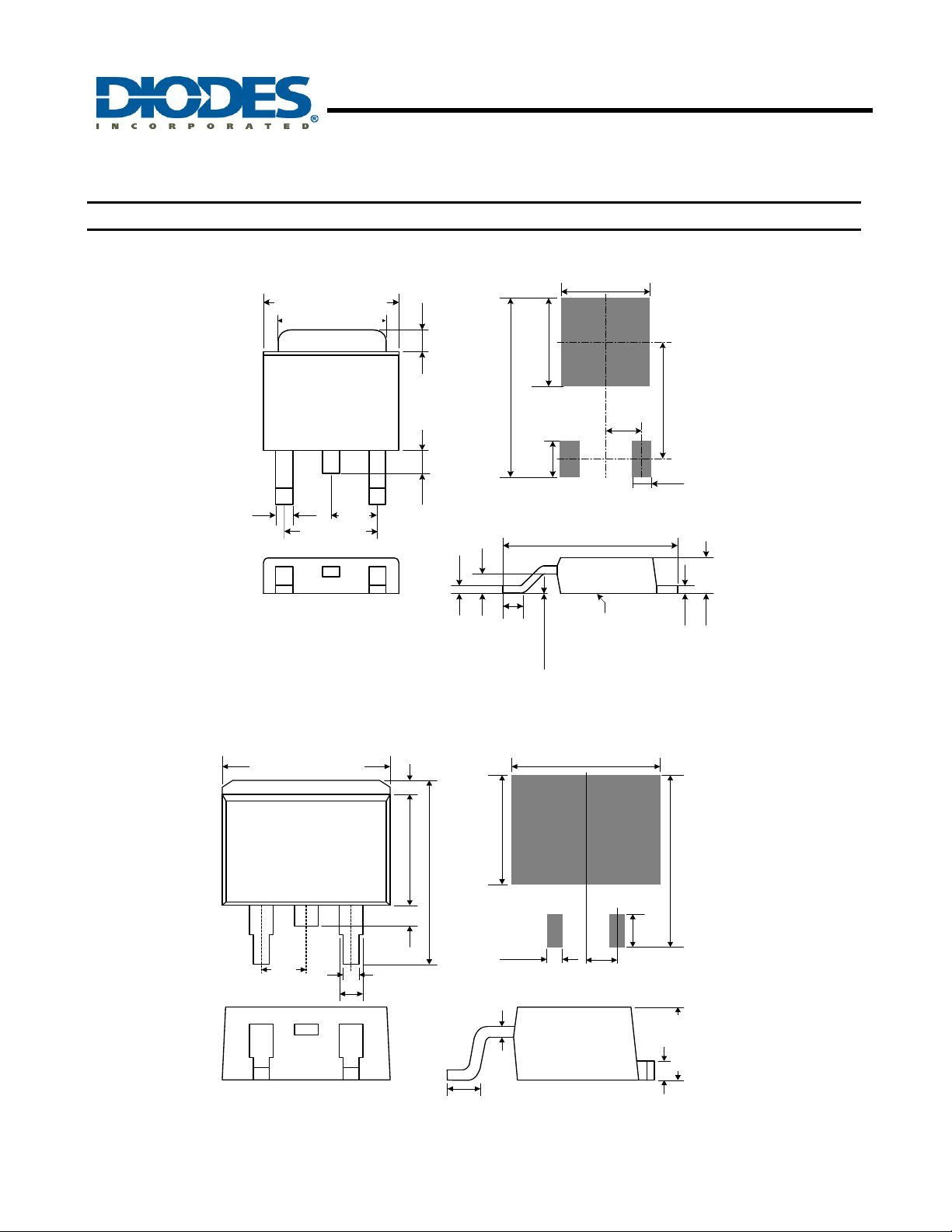
Package Outline Dimensions (All Dimensions in mm)
(1) Package type: TO252-3L
6.354/6.80 Typ 6.58
5.20/5.50 Typ 5.35
0.88/1.27
AP1086
FIXED-MODE REGULATOR
5.6
5.6
0.61 Typ
(2) Package type: TO263-3L
9.65/10.29 Typ 9.97
2.28
BSC.
4.57 BSC.
Typ 5.57
5.40/6.20
0.64/1.02
Typ 0.83
0.45/0.58
Typ 0.52
2.92
Typ 1.30
11.0
2.25
2.0
7.2
Land Pattern Recommendation (Unit: mm)
0.89/
1.14
9.00/10.40 Typ 9.70
0.51
9.1
SEATING
SEE NOTE2
10.9
PLANE
0.45/0.58
Typ 0.52
1.2
2.18/2.40
Typ 2.29
BSC.
AP1086
Document number: DS31028 Rev. 6 - 2
2.54
8.65/9.65 Typ 9.15
14.61/15.88 Typ 15.24
Typ
1.78
1.52
1.27/
0.51/0.99 Typ 0.75
1.14/1.40 Typ1.27
2.28/2.80 Typ 2.54
www.diodes.com
3
1.3
Land Pattern Recommendation (Unit: mm)
0.38 Typ
8 of 10
2.54
15.7
Typ 4.45
4.06/4.83
Typ 1.27
1.14/1.40
June 2010
© Diodes Incorporated
Page 9
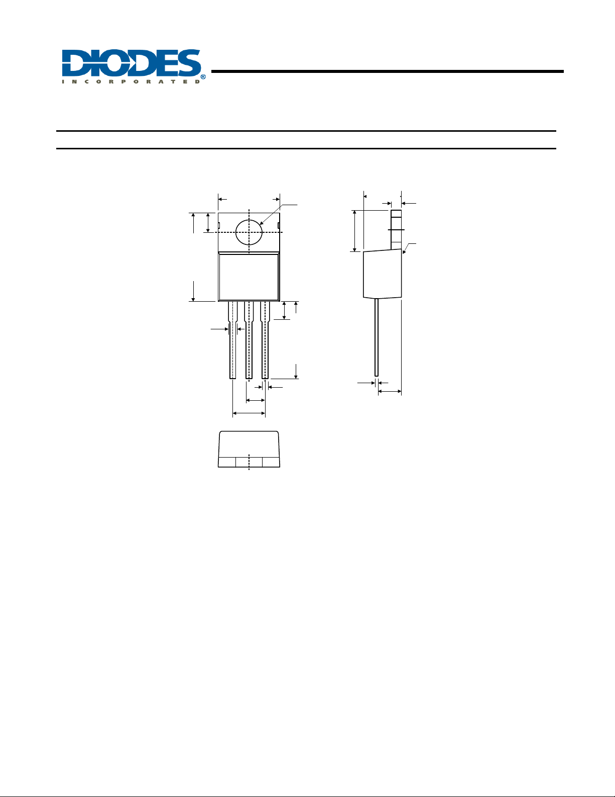
Package Outline Dimensions (Continued)
(3) Package type: TO220-3L
2.54/3.43
Typ 2.98
Typ 15.35
14.20/16.50
1.14/1.78
Typ 1.46
9.70/10.70
Typ 10.20
AP1086
1.5A LOW DROPOUT POSITIVE ADJUSTABLE OR
FIXED-MODE REGULATOR
3.53/4.09
Typ 3.81
3.66/6.35
Typ 5.00
3.55/4.85
Typ 4.20
5.84/6.86
Typ 6.35
0.51/1.40
Typ 0.95
SEATING PLANE
Typ 13.72
12.72/14.72
0.31/1.14
Typ 0.72
2.03/2.92
Typ 2.48
4.83/5.33
Typ 5.08
0.51/1.14
Typ 0.83
2.99/2.79
Typ 2.54
AP1086
Document number: DS31028 Rev. 6 - 2
9 of 10
www.diodes.com
June 2010
© Diodes Incorporated
Page 10

AP1086
1.5A LOW DROPOUT POSITIVE ADJUSTABLE OR
FIXED-MODE REGULATOR
IMPORTANT NOTICE
DIODES INCORPORATED MAKES NO WARRANTY OF ANY KIND, EXPRESS OR IMPLIED, WITH REGARDS TO THIS
DOCUMENT, INCLUDING, BUT NOT LIMITED TO, THE IMPLIED WARRANTIES OF MERCHANTABILITY AND FITNESS FOR A
PARTICULAR PURPOSE (AND THEIR EQUIVALENTS UNDER THE LAWS OF ANY JURISDICTION).
Diodes Incorporated and its subsidiaries reserve the right to make modifications, enhancements, improvements, corrections or other
changes without further notice to this document and any product described herein. Diodes Incorporated does not assume any liability
arising out of the application or use of this document or any product described herein; neither does Diodes In corporated convey any
license under its patent or trademark rights, nor the rights of others. Any Customer or user of this documen t or products described
herein in such applications shall assume all risks of such use and will agree to hold Diodes Incorporated and all the companies
whose products are represented on Diodes Incorporated website, harmless against all damages.
Diodes Incorporated does not warrant or accept any liability whatsoever in respect of any products purchased through unauthorized
sales channel.
Should Customers purchase or use Diodes Incorporated products for any unintended or unauthorized application, Customers shall
indemnify and hold Diodes Incorporated and its representatives harmless against all claims, damages, expenses, and attorney fees
arising out of, directly or indirectly, any claim of personal injury or death associated with such unintended or unauthorized application.
Products described herein may be covered by one or more United States, international or foreign p atents pending. Product names
and markings noted herein may also be covered by one or more United States, international or foreign trademarks.
LIFE SUPPORT
Diodes Incorporated products are specifically not authorized for use as critical components in life support devices or systems without
the express written approval of the Chief Executive Officer of Diodes Incorporated. As used herein:
A. Life support devices or systems are devices or systems which:
1. are intended to implant into the body, or
2. support or sustain life and whose failure to perform when properly used in accordance with instructions for use provided
in the labeling can be reasonably expected to result in significant injury to the user.
B. A critical component is any component in a life support device or system whose failure to perform can b e reasonably expected
to cause the failure of the life support device or to affect its safety or effectiveness.
Customers represent that they have all necessary expertise in the safety and regulatory ramifications of their life support dev ices or
systems, and acknowledge and agree that they are solely responsible for all legal, regulatory and safety-related requirements
concerning their products and any use of Diodes Incorporated products in such safety-critical, life support devices or systems,
notwithstanding any devices- or systems-related information or support that may be provided by Diodes Incorporated. Further,
Customers must fully indemnify Diodes Incorporated and its representatives against any damages arising out of the use of Diodes
Incorporated products in such safety-critical, life support devices or systems.
Copyright © 2010, Diodes Incorporated
www.diodes.com
AP1086
Document number: DS31028 Rev. 6 - 2
10 of 10
www.diodes.com
June 2010
© Diodes Incorporated
 Loading...