

Page 1
A
L5801
100V, ADJUSTABLE CURRENT SINK LINEAR LED DRIVER
EXT
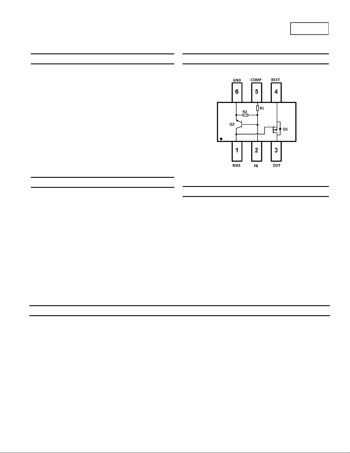
Pin Assignments
Applications
• Linear LED Drivers
• LED Signs
• Offline LED Luminaries
(Top View)
SOT26
Description
The AL5801 combines a 100V N-channel MOSFET with a prebiased NPN transistor to make a simple, small footprint LED driver.
The LED current is set by an external resistor connected from R
pin (4) to GND pin (6). The internal pre-biased transistor develops
approximately 0.56V across the external resistor.
The AL5801 open-drain output can operate from 1.1V to 100V
enabling it to operate 5V to 100V power supplies without additional
components.
PWM dimming of the LED current can be achieved by driving the
BIAS pin (1) with an external, open-collector NPN transistor or
open-drain N-channel MOSFET.
The AL5801 is available in a SOT26 package and is ideal for driving
LED currents up to 350mA.
Features
• Feedback Pin Reference Voltage V
• -40°C to +125°C Temperature Range
• 1.1V to 100V Open-Drain Output
• Negative temperature V
the LED current at high temperatures
• Low thermal impedance SOT26 package with copper lead
frame
• Lead-Free Finish; RoHS Compliant (Notes 1 & 2)
• Halogen and Antimony Free. “Green” Device (Note 3)
• Qualified to AEC-Q101 Standards for High Reliability
Notes: 1. EU Directive 2002/95/EC (RoHS) & 2011/65/EU (RoHS 2) compliant. All applicable RoHS exemptions applied.
2. See http://www.diodes.com for more information about Diodes Incorporated’s definitions of Halogen- and Antimony-free, "Green" and Lead-free.
3. Halogen- and Antimony-free "Green” products are defined as those which contain <900ppm bromine, <900ppm chlorine (<1500ppm total Br + Cl)
and <1000ppm antimony compounds.
co-efficient automatically reduces
RSET
= 0.56V at +25°C
RSET
Typical Applications Circuit
AL5801
Document number: DS35555 Rev. 3 - 2
1 of 11
www.diodes.com
July 2012
© Diodes Incorporated
Page 2
A
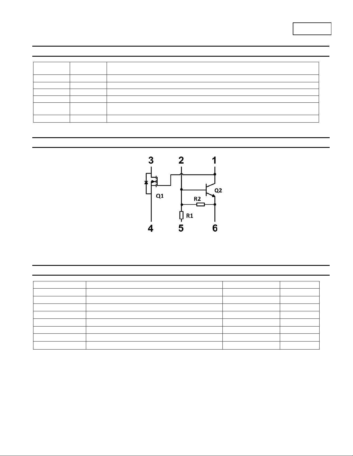
Pin Descriptions
Pin
Number
1 BIAS Biases the open-Drain output MOSFET
2 FB Feedback pin
3 OUT Open-Drain LED driver output
4 R
5 COMP
6 GND Ground refe rence point for setting the LED current
Pin
Name
Current sense pin. LED current sensing resistor should be connected from here to GND
EXT
Compensation pin. Connect COMP pin to REXT pin and insert a 1nF ceramic capacitor from COMP
pin to FB pin for improved transient stability
Functional Block Diagram
L5801
Function
Figure 1 Block Diagram
Absolute Maximum Ratings (@T
Symbol Characteristics Values Unit
V
OUT
V
BIAS
VFB
V
COMP
V
REXT
I
OUT
TJ
TST
Note: 4. With pins 5 and 6 connected together.
These are stress ratings only. Operation outside the absolute maximum ratings may cause device failure.
Operation at the absolute maximum rating for extended periods may reduce device reliability.
Output voltage relative to GND 100 V
BIAS voltage relative to GND (Note 4) 20 V
FB voltage relative to GND 6 V
COMP voltage relative to GND 6 V
REXT voltage relative to GND 6 V
Output current 350 mA
Operating junction temperature -40 to +150 °C
Storage temperature -55 to +150 °C
= +25°C, unless otherwise specified.)
A
AL5801
Document number: DS35555 Rev. 3 - 2
2 of 11
www.diodes.com
July 2012
© Diodes Incorporated
Page 3
A
L5801
Package Thermal Data
Characteristic Symbol Value Unit
Power Dissipation (Note 5) @ TA = +25°C
Power Dissipation (Note 6) @ TA = +25°C
Power Dissipation (Note 7) @ TA = +25°C
Power Dissipation (Note 8) @ TA = +25°C
Thermal Resistance, Junction to Ambient Air (Note 5) @ TA = +25°C
Thermal Resistance, Junction to Ambient Air (Note 6) @ TA = +25°C
Thermal Resistance, Junction to Ambient Air (Note 7) @ TA = +25°C
Thermal Resistance, Junction to Ambient Air (Note 8) @ TA = +25°C
Notes: 5. Device mounted on 15mm x 15mm 2oz copper board.
6. Device mounted on 25mm x 25mm 1oz copper board.
7. Device mounted on 25mm x 25mm 2oz copper board.
8. Device mounted on 50mm x 50mm 2oz copper board.
P
D
R
JA
θ
0.75
0.70
0.85
1.05
165
180
145
120
W
°C/W
Recommended Operating Conditions (@T
= +25°C, unless otherwise specified.)
A
Symbol Parameter Min Max Unit
V
BIAS
V
OUT
I
LED
TA
Note: 9. Subject to ambient temperature, power dissipation and PCB.
NMOSFET Electrical Characteristics: (Q1) (@T
OFF CHARACTERISTICS
Drain-Source Breakdown Voltage
Zero Gate Voltage Drain Current
Gate-Source Leakage
ON CHARACTERISTICS
Gate Threshold Voltage
Static Drain-Source On-Resistance
Forward Transconductance
Diode Forward Voltage
DYNAMIC CHARACTERISTICS
Input Capacitance
Output Capacitance
Reverse Transfer Capacitance
AL5801
Document number: DS35555 Rev. 3 - 2
Supply voltage range 3.5 20
OUT voltage range 1.1 100
V
LED pin current (Note 9) 25 350 mA
Operating ambient temperature range -40 125 °C
= +25°C, unless otherwise specified.)
A
Characteristic Symbol Min Typ Max Unit Test Condition
BV
DSS
I
DSS
I
⎯ ⎯
GSS
V
GS(th)
R
⎯
DS (ON)
g
⎯
fs
V
SD
C
⎯
iss
C
⎯
oss
C
rss
100
⎯ ⎯
2.0
⎯
0.89 1.1 V
⎯
⎯ ⎯
±100
⎯
⎯
⎯
0.85
0.99
0.9
129
14
8
1 µA
4.1 V
⎯
⎯
⎯
⎯
V
V
GS
V
DS
nA
V
GS
V
DS
V
GS
Ω
V
GS
S
V
DS
VGS = 0V, IS = 1.5A
pF
V
pF
pF
DS
f = 1.0MHz
= 0V, ID = 250µA
= 60V, VGS = 0V
= ±20V, VDS = 0V
= VGS, ID = 250µA
= 10V, ID = 1.5A
= 6V, ID = 1A
= 15V, ID = 1A
= 50V, VGS = 0V
3 of 11
www.diodes.com
July 2012
© Diodes Incorporated
Page 4
A
M
A
P
OWER D
PATIO
N
M
P
OWER D
PATIO
N
U
NCTIO
N T
O
N
T
R
Pre-Bias Transistor Electrical Characteristics: (Q2) (@T
Characteristic (Note 10) Symbol Min Typ Max Unit Test Condition
V
Input Voltage
Output Voltage
Output Current
DC Current Gain
Input Resistance
Resistance Ratio
Notes: 10. Short duration pulse test used to minimize self-heating effect.
V
V
I
R
I(off)
I(on)
O(on)
O(off)
G
R
1
2/R1
1
0.4 - - V
- - 1.5 V
- 0.05 0.3 V
- - 0.5
80 - - -
3.2 4.7 6.2 kΩ 8 10 12 - -
Thermal Characteristics
1.2
1.2
= +25°C, unless otherwise specified.)
A
VCC = 5V, IO = 100μA
VCC = 0.3V, IO = 5mA
IO/II = 5mA/0.25mA
μA
VCC = 50V, VI = 0V
VO = 5V, IO = 10mA
L5801
1.0
(W)
ISSI
0.8
0.6
50mm x 50mm
(2oz. FR4)
25mm x 25mm
(2oz. FR4)
15mm x 15mm
(2oz. FR4)
0.4
X
0.2
0
0 25 50 75 100 125 150
TEMPERATURE (°C)
Figur e 2 Derating Cur ve
180
160
140
T = 25°C
A
25mm x 25mm
1oz. FR4
AI
120
100
AMBIE
D = 0.5
80
60
D = 0.2
T = 25°C
A
2oz. FR4
1.0
(W)
0.8
ISSI
0.6
0.4
AX
0.2
0
0 500 1,000 1,500 2,000 2,500
COPPER AREA (mm )
D = 0.1
D = 0.05
Figur e 3 Area vs. Max Power
2
J
40
THERMAL RESISTANCE (°C/W)
Single Pulse
20
0
0.0001 0.001 0.01 0.1 1 10 100 1,000
PULSE WIDTH (s)
Figure 4 Tran si ent Therm al Impedance
AL5801
Document number: DS35555 Rev. 3 - 2
4 of 11
www.diodes.com
July 2012
© Diodes Incorporated
Page 5

A
Typical Performance Characteristics
0.40
0.35
0.30
I = 0.1mA
bias
R = 1.6
Ω
EXT
L5801
400
350
300
I = 0.1mA
bias
0.25
0.20
OUT
I (A)
0.15
R = 3.75
EXT
Ω
0.10
0.05
0
0123
Figure 5 Output Current vs. V
R = 11.6
EXT
R = 22.7
EXT
V (V)
OUT
Ω
Ω
OUT
0.5
T = -40C
°
0.4
A
T = 25C
°
A
0.3
T = 85C
°
OUT
I (A)
0.2
0.1
0
0123
V (V)
OUT
Figure 7 Output Current vs. V
A
I = 0.1mA
bias
R = 1.6
Ω
EXT
OUT
0.07
250
200
OUT
I (mA)
150
100
50
0
110100
Figure 6 Output Current vs. R
Ω
R ()
EXT
EXT
0.20
T = -40C
°
A
0.15
0.10
OUT
I (A)
T = 25C
°
A
T = 85C
°
A
0.05
I = 0.1mA
bias
EXT
Ω
OUT
R = 3.75
0
0246810
V (V)
OUT
Figure 8 Output Current vs. V
0.035
0.06
0.05
0.04
OUT
0.03
I (A)
0.02
0.01
0
0 5 10 15
Figure 9 Output Current vs. V
AL5801
Document number: DS35555 Rev. 3 - 2
T = -40C
A
T = 25C
A
T = 85C
A
V (V)
OUT
°
°
°
I = 0.1mA
bias
R = 11.6
EXT
Ω
OUT
5 of 11
www.diodes.com
OUT
I (A)
0.030
0.025
T = -40C
A
T = 25C
A
0.020
T = 85C
A
0.015
0.010
I = 0.1mA
0.005
0
0 5 10 15 20
V (V)
OUT
bias
R = 22.7
EXT
Figure 10 Output Current vs. V
°
°
°
Ω
OUT
© Diodes Incorporated
July 2012
Page 6
A
Typical Performance Characteristics (cont.)
800
700
600
400
350
300
50mm x 50mm
(2oz. FR4)
L5801
I = 0.1mA
bias
T = 85°C
A
500
400
REXT
V (mV)
300
200
100
0
-50 0 50 100 150
JUNCTION TEMPERATURE ( C)
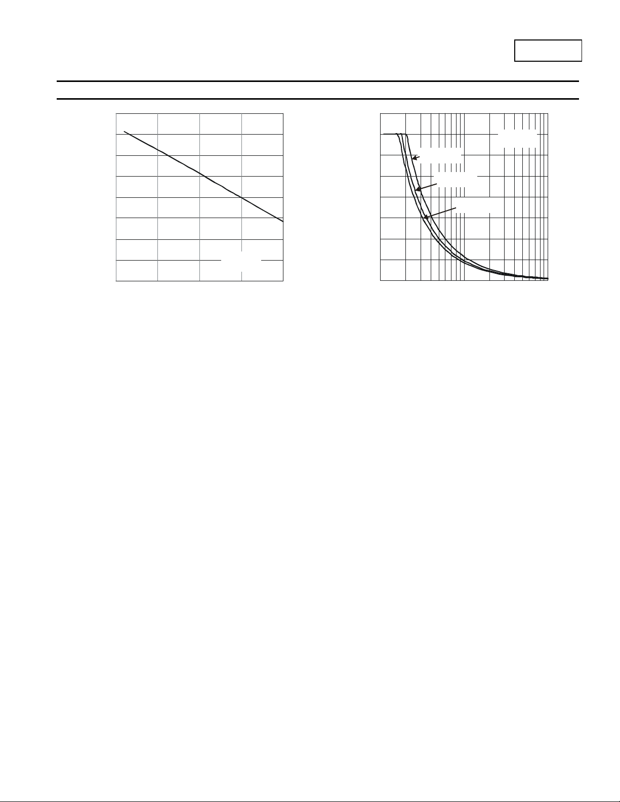
Figure 11 V vs. Junction Temperature
REXT
AL5801
Document number: DS35555 Rev. 3 - 2
I = 0.1mA
bias
= 5V
V
bias
°
6 of 11
www.diodes.com
25mm x 25mm
(2oz. FR4)
15mm x 15mm
(2oz. FR4)
OUT
I (mA)
250
200
150
100
50
0
110100
Figure 12 Output Current vs. V
V (V)
OUT
OUT
July 2012
© Diodes Incorporated
Page 7

A
Application Information
L5801
Figure 13 Typical Application Circuit for
Linear Mode Current Sink LED Driver
The AL5801 is designed for driving high brightness LEDs with typical LED current up to 350mA. It provides a more cost effective way for driving
low current LEDs when compared against more complex switching regulator solutions. Furthermore, it reduces the PCB board area of the
solution because there is no need for external components like inductors, capacitors and/or switching diodes.
Figure 13 shows a typical application circuit diagram for driving an LED or a string of LEDs. The NPN transistor Q2 measures the LED current by
sensing the voltage across an external resistor R
. Q2 uses its VBE as reference to set the voltage across R
EXT
and controls the gate voltage of
EXT
MOSFET Q1. Q1 operates in linear mode to regulate the LED current. The LED current is:
= V
/ R
EXT
where V
is the VBE of Q2. VBE is 0.56V typical at a +25°C device temperature. See Figure 11 for the variation of VBE with Q2’s junc tion
RSET
temperature at I
I
LED
RSET
= 0.1mA. VBE has a negative temperature coefficient which reduces the LED current as the device warms up, protecting the
BIAS
LED(s).
R
should be chosen to drive 0.1mA current into the BIAS pin
BIAS
R
= ( VCC – 3.75V ) / 0.1mA
BIAS
From the above equation, for any required LED current the necessary external resistor R
R
= V
/ I
EXT
RSET
LED
can be calculated from
EXT
The expected linear mode power dissipation must be factored into the design consideration. The power dissipation across the dev ice can be
calculated by taking the maximum supply voltage less the minimum voltage across the LED string.
V
DS(Q1)
= V
CC(max)
– V
LED(min)
– V
RSET
= V
P
D
DS(Q1)
* I
LED
As the output LED current of AL5801 increases so will its power dissipation. The power dissipation will cause the device temperature to rise
above ambient, T
, by an amount determined by the package thermal resistance, R
A
θJA
.
Therefore, the power dissipation supported by the device is dependent upon the PCB board material, the copper area and the ambient
temperature. The maximum dissipation the device can handle is given by:
P
= ( T
D
= +150°C is the maximum device junction temperature. Refer to the thermal characteristic graphs in Figure 2 to 4 for selecting the
T
J(MAX)
J(MAX)
- TA ) / R
θJA
appropriate PCB copper area. Figure 12 shows the current capabilities of the AL5801 at +25°C with different PCB copper area heat sinks.
AL5801
Document number: DS35555 Rev. 3 - 2
7 of 11
www.diodes.com
July 2012
© Diodes Incorporated
Page 8

A
L5801
Constant LED Current Temperture Compensation
Variation in the junction temperature of Q2 will cause variations in the value of controlled LED current I
decreases with increasing temperature at a rate of approximately 2mV/°C. Figure 14 shows a simple temperature compensation network, which
comprises of an NTC thermistor and resistor R
, for stabilizing the LED current.
base
. The base-emitter VBE voltage of Q2
LED
Figure 14 Constant LED Current Temperature Compensation for AL5801
The voltage drop V
is 0.56V at room temperature with 0.1mA I
V
BE(Q2)
With the V
chosen, the sense resistor value for 350mA I
RSET
= V
R
EXT
So a standard resistor value of 1.78Ω with 1% tolerance is used.
The R
resistance of the NTC thermistor at room temperature is recommended as 10kΩ. The value of base resistor R
TH
Q2’s base current is obtained as
I
B(Q2)
When V
is changed to V
BE(Q2)
given by
T
R
= V
TH
At -2mV/°C, V
BE(Q2)
resistance at +85°C to keep the same output current is given by
85
R
TH
The NTC thermistor is chosen for compensation whose resistance is 10kΩ at +25°C and 1.38kΩ at +85°C with a β value of 3530.
Figure 15 shows the I
in the sense resistor R
RSET
/ I
RSET
LED
= ( V
BE
RSET
T
/ (( V
- V
RSET
= 0.62V / 350mA = 1.77Ω
)
/ R
BE(Q2)
BE
base
T
as the temperature increases to TºC, the thermistor resistance at T°C required to compensate this variation is
T
- V
) / R
BE
should be set to be 40 to 100mV higher than the V
EXT
- V
base
, so V
BIAS
/ RTH = ( 0.62V - 0.56 ) / 470Ω - 0.56V / 10kΩ = 72µA
BE(Q2)
- I
)
B(Q2)
is selected to be 0.62V.
RSET
is determined by
LED
at 25ºC. Figure 11 shows the typical
BE(Q2)
is set to be 470Ω.
base
reduces to 0.44V from 0.56V as the temperature increases from +25°C to +85°C. From the above equation, the thermistor’s
= 0.44V / (( 0.62V – 0.44V ) / 470Ω - 72µA ) = 1.4kΩ
variation with temperature with and without temperature compensation.
LED
AL5801
Document number: DS35555 Rev. 3 - 2
Figure 15 LED Current Variation with and
without Temperature Compensation
8 of 11
www.diodes.com
July 2012
© Diodes Incorporated
Page 9

A
PWM Dimming
L5801
(a)
Figure 16 Application Circuits for LED Driver with PWM Dimming Functionality (a) MOSFET driving and (b) Transistor driving
PWM dimming can be achieved by driving the BIAS pin (1). An external open-collector NPN transistor or open-dr ain N-channel M OSFET can b e
used to drive the BIAS pin as shown in Figure 16. Dimming is achieved by turning the LEDs ON and OFF for a portion of a single cycle. The
PWM signal can be provided by a micro-controller or by analog circuitry.
Figure 17 shows the LED current against the PWM signal duty ratio when the AL5801 is used to drive three series connected LEDs from a 12V
supply. The PWM dimming frequency is set to 200Hz. The PWM signal is supplied to the open-Drain small signal MOSFET’s gate as shown in
Figure 16a. The BIAS pin signal is an inversion of the PWM drive to the MOSFET’s gate. Therefore, a PWM signal d ut y cycle of 0% provides the
maximum LED current. Sufficiently large PCB copper area is used for heat sinking of the AL5801 in order to minimize the device self-heating at
+25°C ambient.
(b)
Figure 17 LED Current against PWM Dimming Signal Duty Ratio at 200Hz PWM Frequency
AL5801
Document number: DS35555 Rev. 3 - 2
9 of 11
www.diodes.com
July 2012
© Diodes Incorporated
Page 10
A
Ordering Information
Part Number Qualification
Green
Green
AL5801W6-7 Commercial W6 SOT26 3,000/Tape & Reel -7
AL5801W6Q-7 Automotive W6 SOT26 3,000/Tape & Reel -7
Notes: 11. For packaging details, go to our website at http://www.diodes.com
Package
Code
Packaging
(Note 11)
Quantity Part Number Suffix
7” Tape and Reel
Marking Information
L100 = Product Type Marking Code
YM = Date Code Marking
Y = Year (ex: Y = 2012)
M = Month (ex: 9 = September)
Date Code Key
Year 2012 2013 2014 2015 2016 2017 2018
Code Z A B C D E F
Month Jan Feb Mar Apr May Jun Jul Aug Sep Oct Nov Dec
Code 1 2 3 4 5 6 7 8 9 O N D
Package Outline Dimensions (All dimensions in mm.)
A
B C
K
H
J
D
L
SOT26
Dim Min Max Typ
A 0.35 0.50 0.38
B 1.50 1.70 1.60
C 2.70 3.00 2.80
D
⎯ ⎯
0.95
H 2.90 3.10 3.00
J 0.013 0.10 0.05
K 1.00 1.30 1.10
M
L 0.35 0.55 0.40
M 0.10 0.20 0.15
0° 8°
α
⎯
All Dimensions in mm
Suggested Pad Layout
G
Z
Y
C2
C2
C1
Dimensions Value (in mm)
Z
G
X
Y
C1 2.40
C2
3.20
1.60
0.55
0.80
0.95
X
AL5801
Document number: DS35555 Rev. 3 - 2
10 of 11
www.diodes.com
© Diodes Incorporated
L5801
July 2012
Page 11

A
L5801
DIODES INCORPORATED MAKES NO WARRANTY OF ANY KIND, EXPRESS OR IMPLIED, WITH REGARDS TO THIS DOCUMENT,
INCLUDING, BUT NOT LIMITED TO, THE IMPLIED WARRANTIES OF MERCHANTABILITY AND FITNESS FOR A PARTICULAR PURPOSE
(AND THEIR EQUIVALENTS UNDER THE LAWS OF ANY JURISDICTION).
Diodes Incorporated and its subsidiaries reserve the right to make modifications, enhancements, improvements, corrections or other changes
without further notice to this document and any product described herein. Diodes Incorporated does not assume any liability arising out of the
application or use of this document or any product described herein; neither does Diodes Incorporated convey any license under its patent or
trademark rights, nor the rights of others. Any Customer or user of this document or products described herein in such applications shall assume
all risks of such use and will agree to hold Diodes Incorporated and all the companies whose products are represented on Diodes Incorporated
website, harmless against all damages.
Diodes Incorporated does not warrant or accept any liability whatsoever in respect of any products purchased through unauthorized sales channel.
Should Customers purchase or use Diodes Incorporated products for any unintended or unauthorize d application, Customers shall indemnify and
hold Diodes Incorporated and its representatives harmless against all claims, damages, expenses, and attorney fees arising out of, directly or
indirectly, any claim of personal injury or death associated with such unintended or unauthorized application.
Products described herein may be covered by one or more United States, international or foreign patents pending. Product names and markings
noted herein may also be covered by one or more United States, international or foreign trademarks.
Diodes Incorporated products are specifically not authorized for use as critical components in life support devices or systems without the express
written approval of the Chief Executive Officer of Diodes Incorporated. As used herein:
A. Life support devices or systems are devices or systems which:
1. are intended to implant into the body, or
2. support or sustain life and whose failure to perform when properly used in accordance with instructions for use provided in the
labeling can be reasonably expected to result in significant injury to the user.
B. A critical component is any component in a life support device or system whose failure to perform can be reasonably expected to cause the
failure of the life support device or to affect its safety or effectiveness.
Customers represent that they have all necessary expertise in the safety and regulatory ramifications of their life support devices or systems, and
acknowledge and agree that they are solely responsible for all legal, regulatory and safety-related requirements concerning their products and any
use of Diodes Incorporated products in such safety-critical, life support devices or systems, notwithstanding any devices- or systems-related
information or support that may be provided by Diodes Incorporated. Further, Customers must fully indemnify Diodes Incorporated and its
representatives against any damages arising out of the use of Diodes Incorporated products in such safety-critical, life support devices or systems.
Copyright © 2012, Diodes Incorporated
www.diodes.com
IMPORTANT NOTICE
LIFE SUPPORT
AL5801
Document number: DS35555 Rev. 3 - 2
11 of 11
www.diodes.com
July 2012
© Diodes Incorporated
 Loading...