

Page 1
HIGH SENSITIVITY CMOS HALL-EFFECT LATCH AH921
Data Sheet
General Description
The AH921 is a Hall-effect latch designed in mixed
signal CMOS technology. It is quite suitable for use
in automotive, industrial and consumer applications.
Superior high-temperature performance is made
possible through dynamic offset cancellation, which
reduces the residual offset voltage normally caused
by device over-molding, temperature dependencies,
and thermal stress. The device integrates a voltage
regulator, Hall-voltage generator, small-signal
amplifier, chopper stabilization, schmitt trigger, and
is directly drivable by the output.
An on-board regulator permits operation with supply
voltage from 3.5V to 24V.
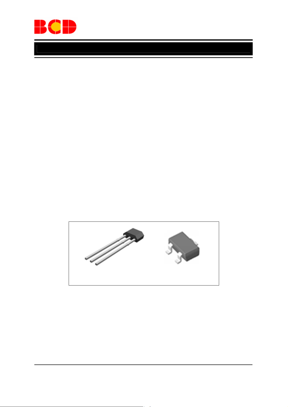
The AH921 is available in TO-92S-3 and SOT-2 3-3
packages, which are optimized for most applications.
TO-92S-3 SOT-23-3
Features
• Wide Operating Voltage Range from 3.5 to 24V
• Symmetrical Switch Points
• Chopper-stabilized Amplifier Stage
• Superior Temperature Stability
• Compact Size
• Built-in Pull-up Resistor
• ESD Rating: 3500V (Human Body Model)
Applications
• Brushless DC Motor Commutation
• Brushless DC Fan
• Solid-state Switch
• Revolution Counting
• Speed Detection
• High Sensitivity and Unconnected Switch
Figure 1. Package Types of AH92 1
Jul. 2011 Rev. 1. 2 BCD Semiconductor Manufacturing Limited
1
Page 2
Data Sheet
HIGH SENSITIVITY CMOS HALL-EFFECT LATCH AH921
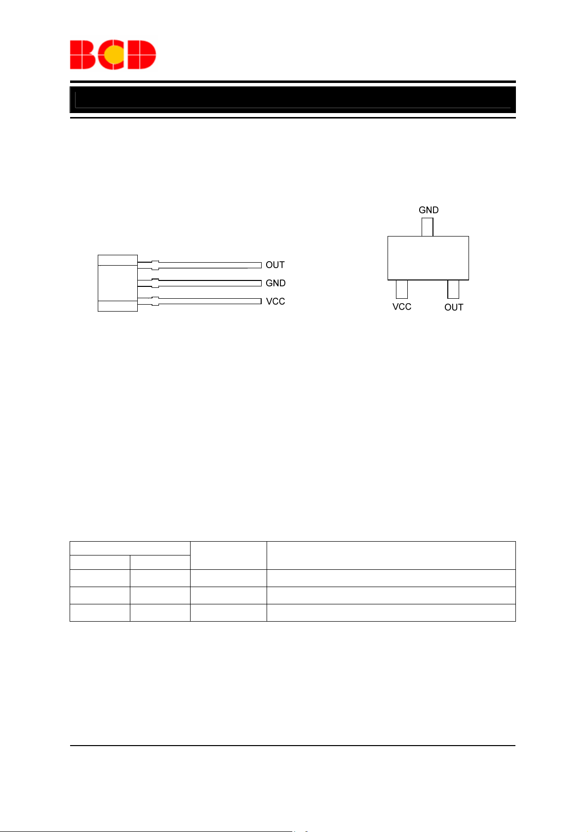
Pin Configuration
Z3 Package N Package
(TO-92S-3) (SOT-23-3)
3
3
2
1
(Front View) (Top View)
Figure 2. Pin Configuration of AH921
Pin Description
Pin Number
TO-92S-3 SOT-23-3
1 1 VCC Supply voltage
Pin Name Function
21
2 3 GND Ground pin
3 2 OUT Output pin
Jul. 2011 Rev. 1. 2 BCD Semiconductor Manufacturing Limited
2
Page 3
Data Sheet
HIGH SENSITIVITY CMOS HALL-EFFECT LATCH AH921
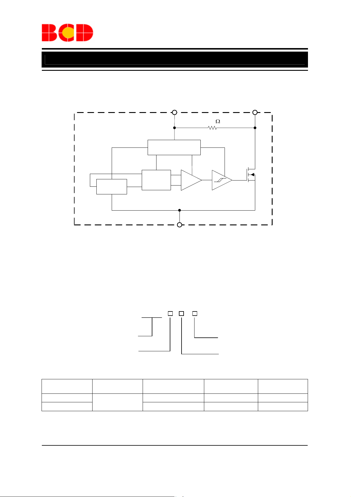
Functional Block Diagram
A (B)
A for TO-92S-3
B for SOT-23-3
Hall Sense
VCC
1 (1)
Reference Voltage
Chopper
Switch
2 (3)
AMP
100k
GND
Figure 3. Functional Block Diagram of AH921
OUT
3 (2)
Ordering Information
AH921 -
Circuit Type
Package
Z3: TO-92S-3
N: SOT-23-3
G1: Green
TR: Tape & Reel
Blank: Bulk
Package
TO-92S-3 AH921Z3-G1 921 Bulk
SOT-23-3
Temperature
Range
-40 to 125°C
Part Number Marking ID Packing Type
AH921NTR-G1 GS6 Tape & Reel
BCD Semiconductor's Pb-free products, as designated with "G1" suffix in the part number, are RoHS
compliant and green.
Jul. 2011 Rev. 1. 2 BCD Semiconductor Manufacturing Limited
3
Page 4
Data Sheet
HIGH SENSITIVITY CMOS HALL-EFFECT LATCH AH921
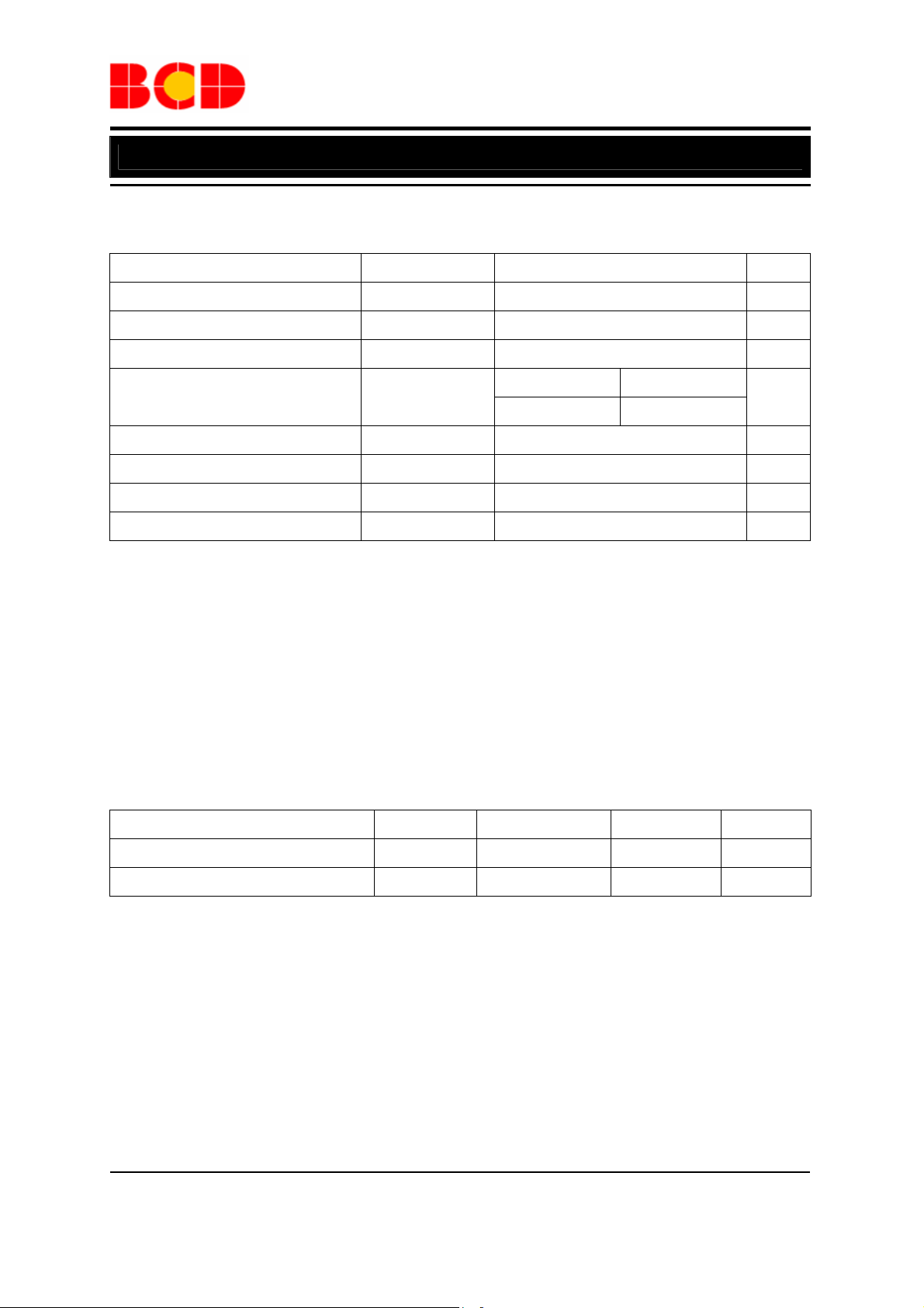
Absolute Maximum Ratings (Note 1)
Parameter Symbol Value Unit
Supply Voltage VCC 28 V
Supply Current (Fault) ICC 5 mA
Output current (Continuous) I
Power Dissipation
Operating T em perature TA -50 to 150
Storage Temperature T
Maximum Junction Temperature TJ (Max) 165
ESD (Human Body Model) ESD 3500 V
25 mA
OUT
P
D
-65 to 150
STG
TO-92S-3 400
SOT-23-3
230
mW
ºC
ºC
ºC
Note 1: Stresses greater than those listed under “Absolute Maximum Ratings” may cause permanent damage to
the device. These are stress ratings only, and functional operation of the device at these or any other conditions
beyond those indicated under “Recommended Operating Conditions” is not implied. Exposure to “Absolute
Maximum Ratings” for extended periods may affect device reliability.
Recommended Operating Conditions
Parameter Symbol Min Max Unit
Supply Voltage V
Operating Temperature TA -40 125 ºC
CC
3.5 24 V
Jul. 2011 Rev. 1. 2 BCD Semiconductor Manufacturing Limited
4
Page 5
Data Sheet
HIGH SENSITIVITY CMOS HALL-EFFECT LATCH AH921
Electrical Characteristics
V
=12V, TA=25°C, unless otherwise specified.
CC
Parameter Symbol Conditions Min Typ Max Unit
Supply Voltage VCC Operating 3.5 12 24 V
Supply Current ICC
VCC=12V, B<BRP 3.0 5.0 mA
V
=12V, B>BOP 3.0 5.0 mA
CC
Saturation Voltage V
Output Leakage Current I
Output Rising Time t
Output Falling Time t
I
SAT
LEAKAGE
FALLING
VCC=V
CL=20pF 0.4 2
RISING
CL=20pF 0.4 2
=20mA, B>BOP 185 500 mV
OUT
=24V, B<BRP 0.1 10
OUT
μA
μs
μs
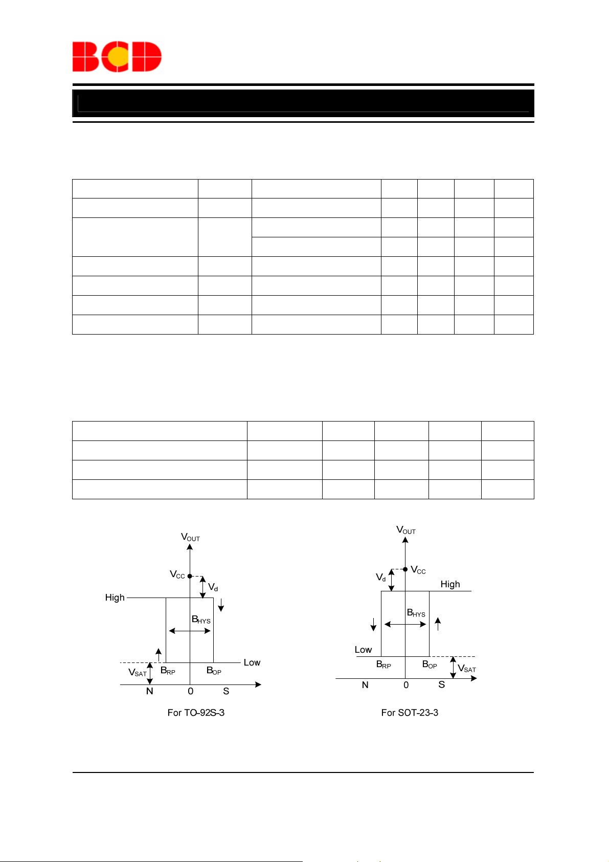
Magnetic Characteristics
V
=12V, TA=25°C, unless otherwise specified.
CC
Parameter Symbol Min Typ Max Unit
Operating Point BOP 5 22 40 Gauss
Releasing Point BRP -40 -22 -5 Gauss
Hysteresis B
45 Gauss
HYS
Figure 4. Magnetic Flux Density of AH921
Jul. 2011 Rev. 1. 2 BCD Semiconductor Manufacturing Limited
5
Page 6
Data Sheet
HIGH SENSITIVITY CMOS HALL-EFFECT LATCH AH921
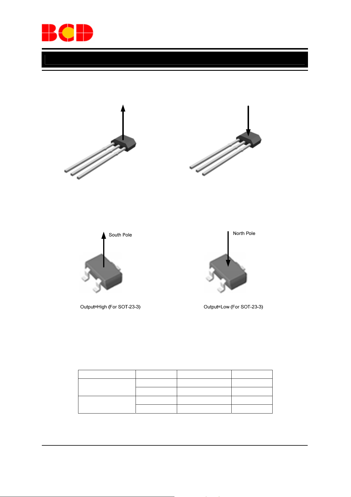
Magnetic Characteristics (Continued)
South Pole
Output=Low (For TO-92S-3)
Output=High (For TO-92S-3)
North Pole
Figure 5. Output Status vs. Magnetic Pole
Package Type
TO-92S-3
SOT-23-3
Jul. 2011 Rev. 1. 2 BCD Semiconductor Manufacturing Limited
Parameter Test condition Output
South Pole B>BOP Low
North Pole B<B
South Pole B>BOP High
North Pole B<B
Table 1. Output Status vs. Magnetic Pole
6
High
RP
Low
RP
Page 7
Data Sheet
HIGH SENSITIVITY CMOS HALL-EFFECT LATCH AH921
Magnetic Characteristics (Continued)
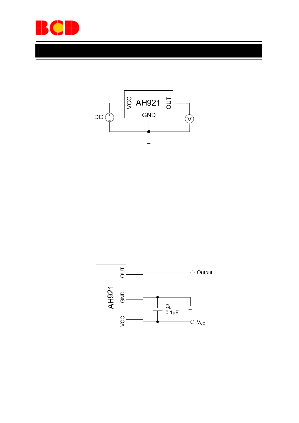
Figure 6. Magnetic Thresholds
Note 2: BOP is determined by putting the device under magnetic field swept from BRP(Min) to BOP(Max) until the
output is switched on.
Note 3: B
output is switched off.
is determined by putting the device under magnetic field swept from BOP(Max) to BRP(Min) until the
RP
Test Circuit and Test Conditions
Figure 7. Test Circuit of AH921
Jul. 2011 Rev. 1. 2 BCD Semiconductor Manufacturing Limited
7
Page 8
Data Sheet
HIGH SENSITIVITY CMOS HALL-EFFECT LATCH AH921
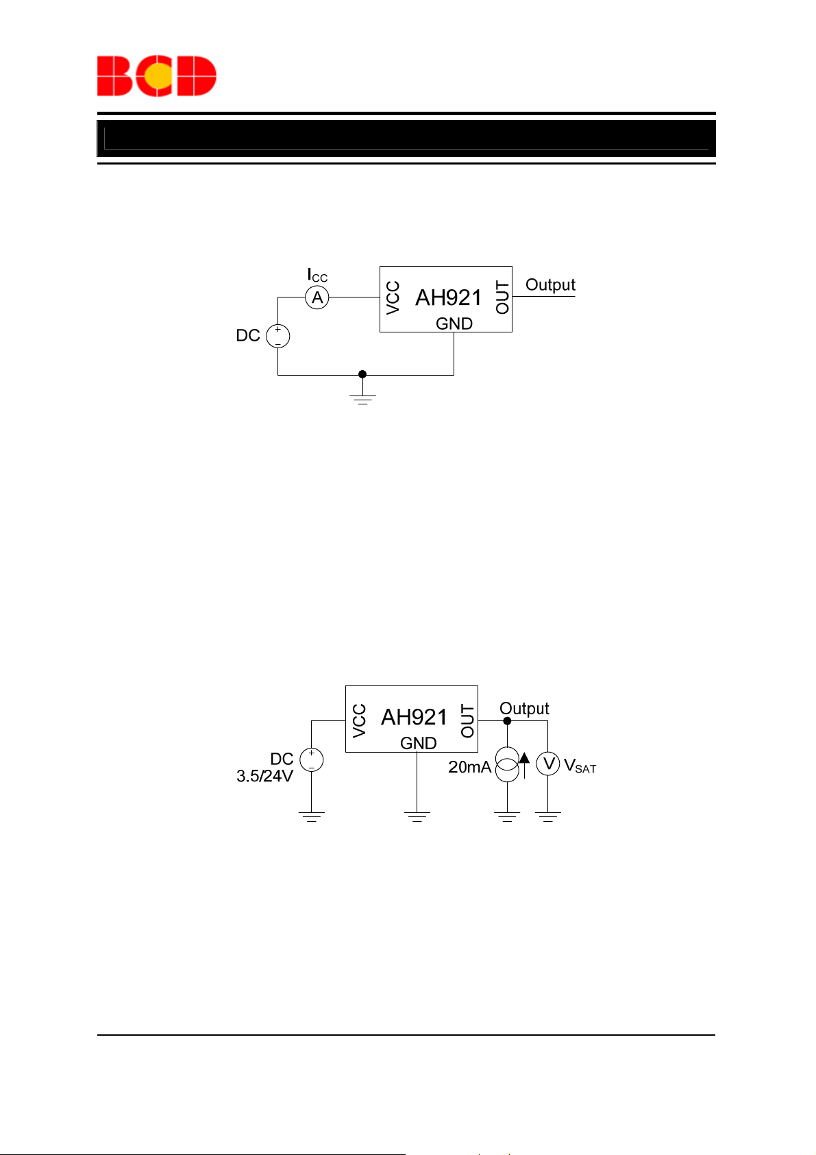
Test Circuit and Test Conditions (Continued)
Figure 8. Test Condition of AH921 (Supply Current)
Note 4: Output initial status is low when powering on.
Note 5: The supply current I
represents the average supply current. The output is open during measurement.
CC
Note 6: The device is put under the magnetic field: B<B
RP.
Figure 9. Test Condition of AH921 (Output Saturation Voltage)
Note 7: The output saturatio n volt a ge V
Note 8: The device is put under the magnetic field: B>B
Jul. 2011 Rev. 1. 2 BCD Semiconductor Manufacturing Limited
is measured at VCC=3.5V and VCC=24V.
SAT
OP.
8
Page 9
Data Sheet
HIGH SENSITIVITY CMOS HALL-EFFECT LATCH AH921
Test Circuit and Test Conditions (Continued)
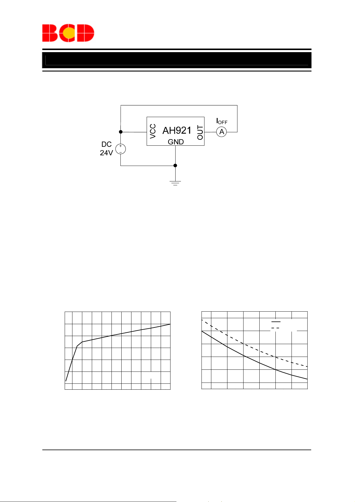
Figure 10. Test Condition of AH921 (Output Leakage Current)
Note 9: The device is put under the magnetic field: B<B
RP.
Typical Performance Characteristics
4.0
3.5
3.0
2.5
(mA)
CC
I
2.0
1.5
1.0
4 6 8 10 12 14 16 18 20 22 24
VCC (V)
TA=25oC
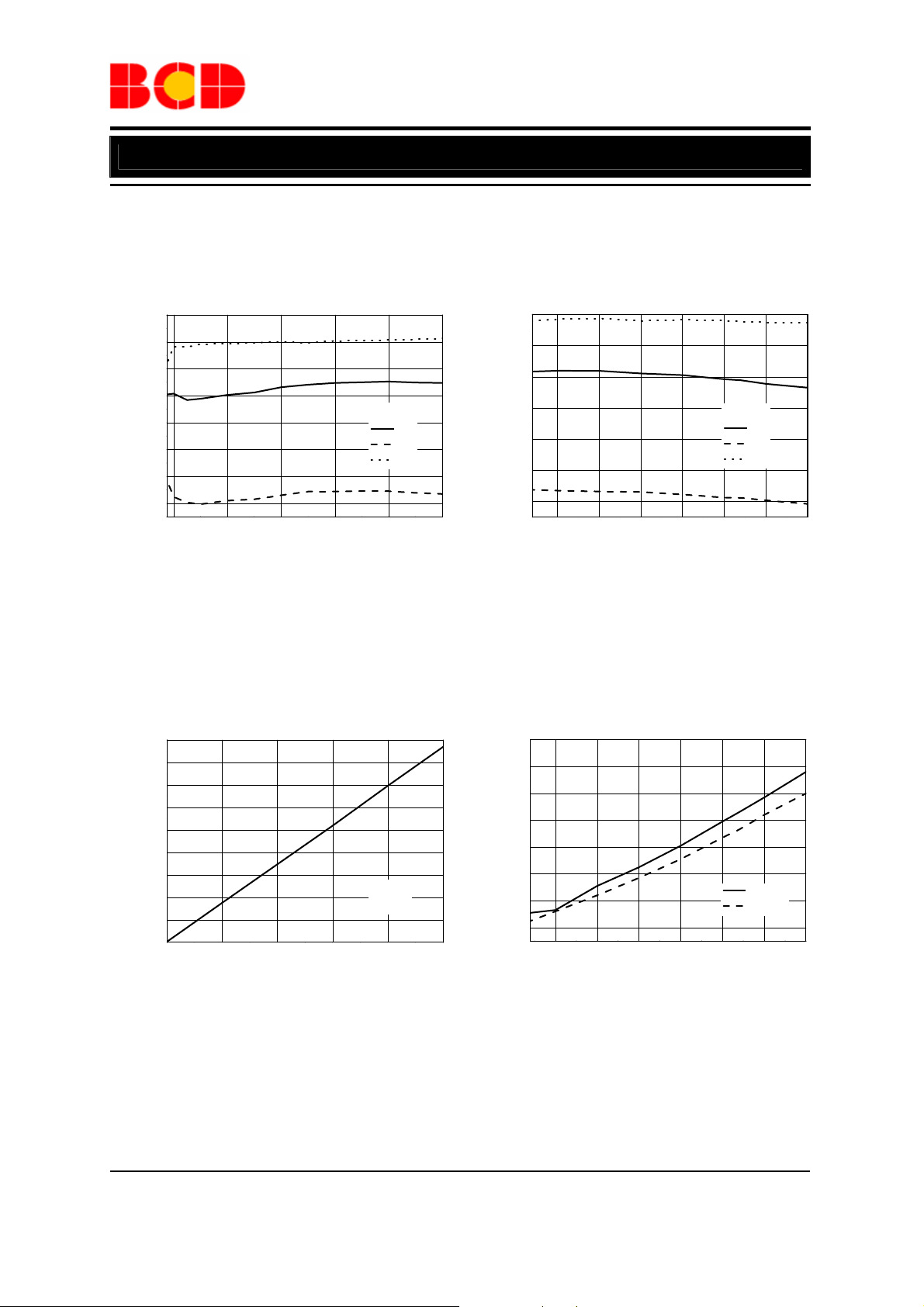
Figure 11. I
vs. VCC Figure 12. ICC vs. TA
CC
Jul. 2011 Rev. 1. 2 BCD Semiconductor Manufacturing Limited
4.0
3.5
VCC=5V
VCC=12V
3.0
(mA)
CC
2.5
I
2.0
1.5
-25 0 25 50 75 100 125
TA (oC)
9
Page 10
Data Sheet
HIGH SENSITIVITY CMOS HALL-EFFECT LATCH AH921
Typical Performance Characteristics (Continued)
40
50
40
30
20
(Gauss)
HYS
10
/B
RP
/B
0
OP
B
-10
-20
4 8 12 16 20 24
VCC (V)
TA=25oC
B
OP
B
RP
B
HYS
30
20
(Gauss)
10
HYS
/B
RP
0
/B
OP
B
-10
-20
-25 0 25 50 75 100 125
TA (oC)
VCC=12V
B
B
B
OP
RP
HYS
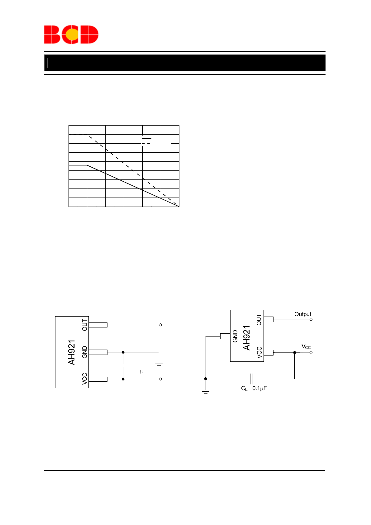
Figure 13. B
OP/BRP/BHYS
vs. VCC Figure 14. BOP/BRP/B
HYS
vs. TA
180
160
140
120
100
(mV)
80
SAT
V
60
40
20
0
0 5 10 15 20 25
I
(mA)
OUT
TA=25oC
VCC=12V
240
220
200
180
(mV)
160
SAT
V
140
120
100
-25 0 25 50 75 100 125
TA (oC)
VCC=5V
VCC=12V
Figure 15. V
SAT
vs. I
Figure 16. V
OUT
SAT
vs. TA
Jul. 2011 Rev. 1. 2 BCD Semiconductor Manufacturing Limited
10
Page 11
Data Sheet
HIGH SENSITIVITY CMOS HALL-EFFECT LATCH AH921
Typical Performance Characteristics (Continued)
450
400
350
300
250
(mW)
D
200
P
150
100
50
0
0 255075100125150
TA (oC)
SOT-23-3
TO-92S-3
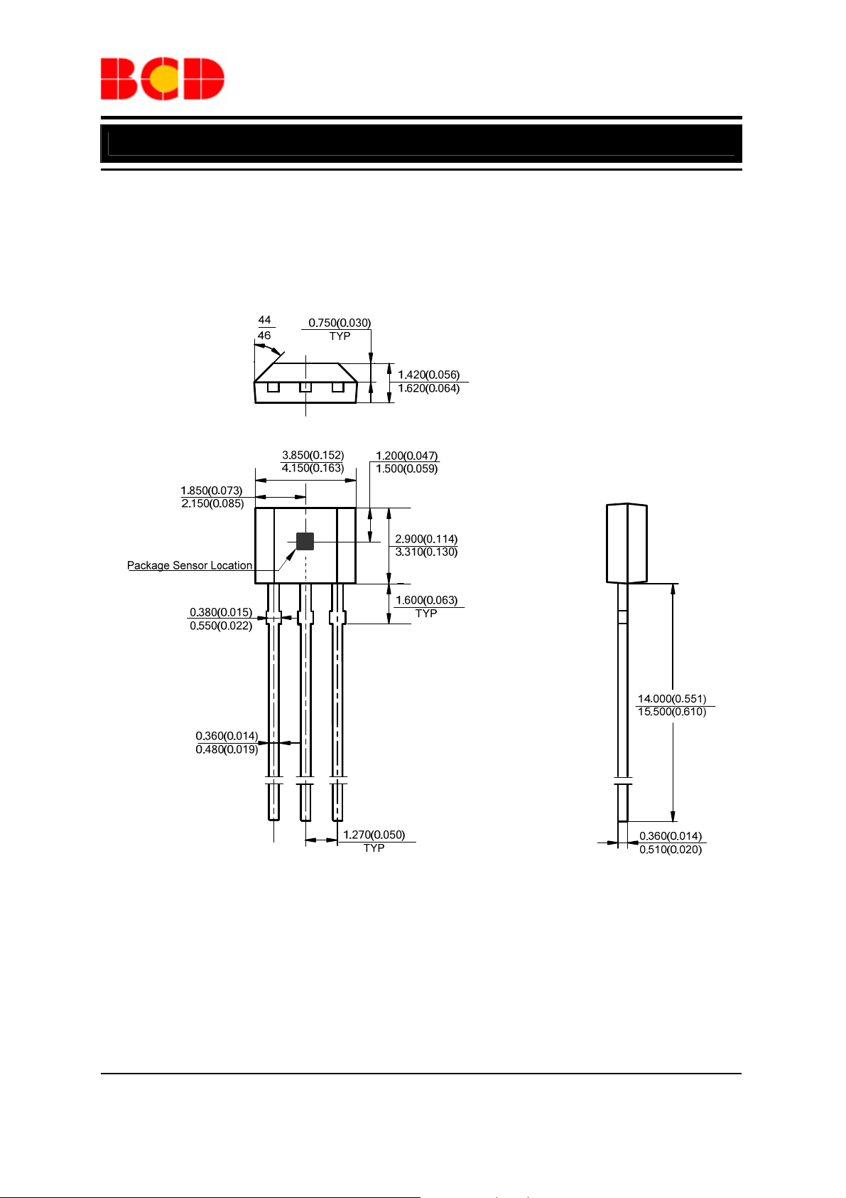
Figure 17. P
vs. TA
D
T ypical Application
Output
C
L
0.1 F
V
CC
Figure 18. Typical Application Circuit of AH921
Jul. 2011 Rev. 1. 2 BCD Semiconductor Manufacturing Limited
11
Page 12
Data Sheet
HIGH SENSITIVITY CMOS HALL-EFFECT LATCH AH921
Mechanical Dimensions
TO-92S-3 Unit: mm(inch)
°
°
Jul. 2011 Rev. 1. 2 BCD Semiconductor Manufacturing Limited
12
Page 13
Data Sheet
HIGH SENSITIVITY CMOS HALL-EFFECT LATCH AH921
Mechanical Dimensions (Continued)
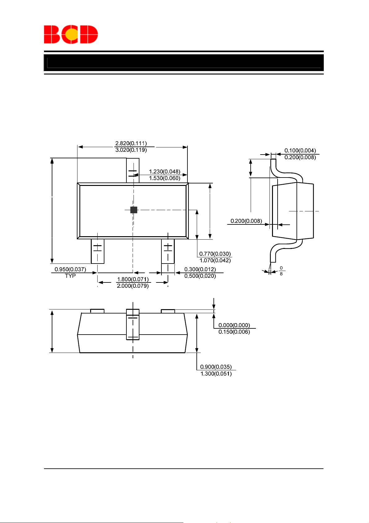
SOT-23-3 Unit: mm(inch)
0.300(0.012)
0.600(0.024)
1.500(0.059)
1.700(0.067)
2.650(0.104)
2.950(0.116)
°
°
MAX.
1.450(0.057)
Jul. 2011 Rev. 1. 2 BCD Semiconductor Manufacturing Limited
13
Page 14

BCD Semiconductor Manufacturing Limited
IMPORTANT NOTICE
IMPORTANT NOTICE
BCD Semiconductor Manufacturing Limited reserves the right to make changes without further notice to any products or specifi-
BCD Semiconductor Manufacturing Limited reserves the right to make changes without further notice to any products or specifi-
cations herein. BCD Semiconductor Manufacturing Limited does not assume any responsibility for use of any its products for any
cations herein. BCD Semiconductor Manufacturing Limited does not assume any responsibility for use of any its products for any
particular purpose, nor does BCD Semiconductor Manufacturing Limited assume any liability arising out of the application or use
particular purpose, nor does BCD Semiconductor Manufacturing Limited assume any liability arising out of the application or use
of any its products or circuits. BCD Semiconductor Manufacturing Limited does not convey any license under its patent rights or
of any its products or circuits. BCD Semiconductor Manufacturing Limited does not convey any license under its patent rights or
other rights nor the rights of others.
other rights nor the rights of others.
http://www.bcdsemi.com
MAIN SITE
MAIN SITE
- Headquarters
BCD Semiconductor Manufacturing Limited
BCD Semiconductor Manufactur ing Limited
- Wafer Fab
No. 1600, Zi Xing Road, Shanghai ZiZhu Science-based Industrial Park, 200241, China
Shanghai SIM-BCD Semiconductor Manufacturing Limited
Tel: +86-21-24162266, Fax: +86-21-24162277
800, Yi Shan Road, Shanghai 200233, China
Tel: +86-21-6485 1491, Fax: +86-21-5450 0008
REGIONAL SALES OFFICE
Shenzhen Office
REGIONAL SALES OFFICE
Shanghai SIM-BCD Semiconductor Manufacturing Co., Ltd., Shenzhen Office
Shenzhen Office
Unit A Room 1203, Skyworth Bldg., Gaoxin Ave.1.S., Nanshan District, Shenzhen,
Shanghai SIM-BCD Semiconductor Manufacturing Co., Ltd. Shenzhen Office
China
Advanced Analog Circuits (Shanghai) Corporation Shenzhen Office
Tel: +86-755-8826 7951
Room E, 5F, Noble Center, No.1006, 3rd Fuzhong Road, Futian District, Shenzhen 518026, China
Fax: +86-755-8826 7865
Tel: +86-755-8826 7951
Fax: +86-755-8826 7865
- Wafer Fab
BCD Semiconductor Manufacturing Limited
Shanghai SIM-BCD Semiconductor Manufacturing Co., Ltd.
- IC Design Group
800 Yi Shan Road, Shanghai 200233, China
Advanced Analog Circuits (Shanghai) Corporation
Tel: +86-21-6485 1491, Fax: +86-21-5450 0008
8F, Zone B, 900, Yi Shan Road, Shanghai 200233, China
Tel: +86-21-6495 9539, Fax: +86-21-6485 9673
Taiwan Office
BCD Semiconductor (Taiwan) Company Limited
Taiwan Office
4F, 298-1, Rui Guang Road, Nei-Hu District, Taipei,
BCD Semiconductor (Taiwan) Company Limited
Tai wan
4F, 298-1, Rui Guang Road, Nei-Hu District, Taipei,
Tel: +886-2-2656 2808
Taiwan
Fax: +886-2-2656 2806
Tel: +886-2-2656 2808
Fax: +886-2-2656 2806
USA Office
BCD Semiconductor Corp.
USA Office
30920 Huntwood Ave. Hayward,
BCD Semiconductor Corporation
CA 94544, USA
30920 Huntwood Ave. Hayward,
Tel : +1-510-324-2988
CA 94544, U.S.A
Fax: +1-510-324-2788
Tel : +1-510-324-2988
Fax: +1-510-324-2788
 Loading...