

Page 1
A
H373
INTERNAL PULL-UP HALL EFFECT LATCH
Description
AH373 is a single-digital-output Hall-Effect latch sensor with internal
pull-up resistor for high temperature operation. The device includes
an on-chip Hall voltage generator for magnetic sensing, an amplifier
to amplify Hall voltage, and a comparator to provide switching
hysteresis for noise rejection, and an output driver with a pull-up
resistor. An internal band-gap regulator provides a temperature
compensated supply voltage for internal circuits and allows a wide
operating supply range.
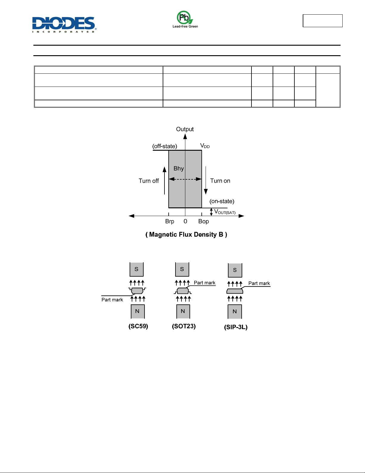
When the magnetic flux density (B) perpendicular to the package is
larger than operate point (Bop), output is switched on (OUT pin is
pulled low). The output state is held on until a magnetic flux density
reversal falls below Brp. When B is less than Brp, the output is
switched off.
The AH373 is available in SIP-3L, SC59 and SOT23 packages.
Features
Bipolar Hall Effect Latch Operation
2.2V to 20V Operating Range
Single Output with Built-in Pull-up Resistor
25mA output Sink Capability
-40C to +125°C Operating Temperature
Industry Standard SIP-3L, SC59 and SOT23 Packages
Totally Lead-Free & Fully RoHS Compliant (Notes 1 & 2)
Halogen and Antimony Free. “Green” Device (Note 3)
Notes: 1. No purposely added lead. Fully EU Directive 2002/95/EC (RoHS) & 2011/65/EU (RoHS 2) compliant.
2. See http://www.diodes.com/quality/lead_free.html for more information about Diodes Incorporated’s definitions of Halogen- and Antimony-free, "Green"
and Lead-free.
3. Halogen- and Antimony-free "Green” products are defined as those which contain <900ppm bromine, <900ppm chlorine (<1500ppm total Br + Cl) and
<1000ppm antimony compounds.
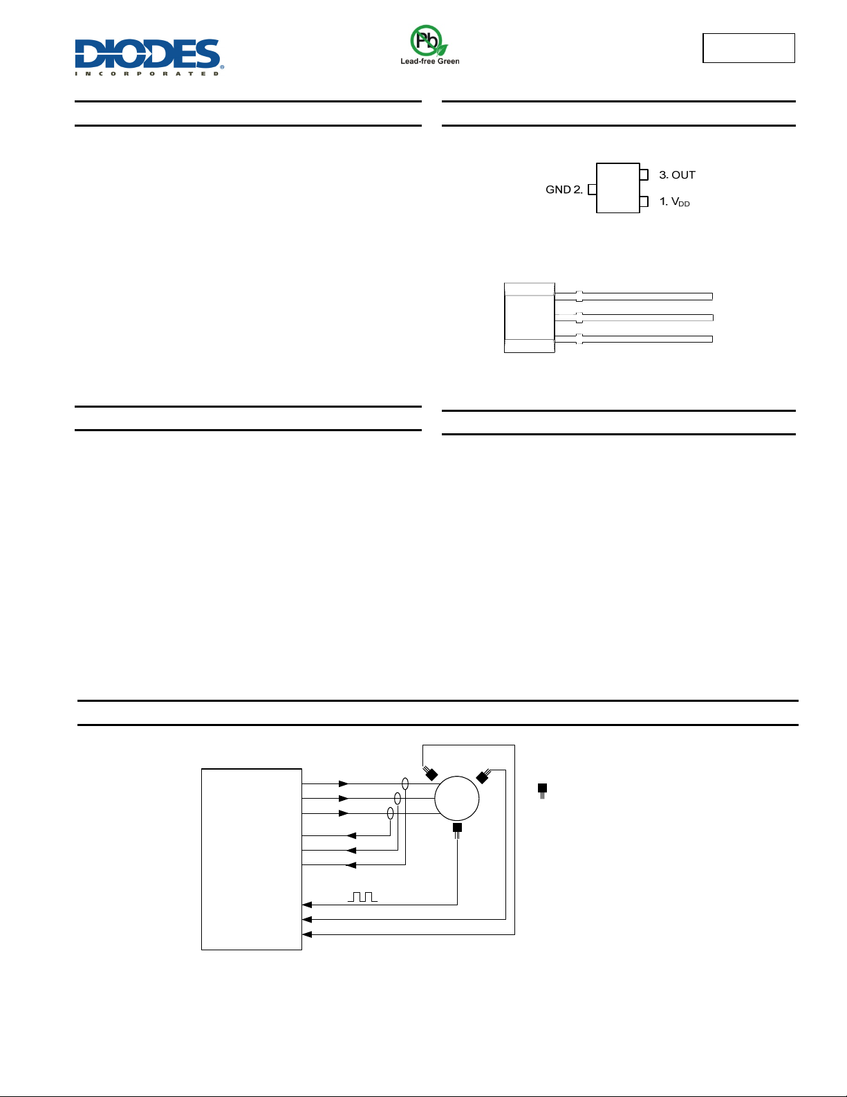
Pin Assignments
(TOP View)
SC59 and SOT23
(TOP View)
SIP-3L
Applications
Rotor Position Sensing for Motor Commutation
Encoder
Speed Measurement – RPM Monitor
Contact-less Current Switch
3.
OUT
GND
2.
V
1.
DD
Typical Application Circuits
Driver
&
Control Logic
Hall Motor Driver
AH373
Document number: Draft DS31173 Rev. 11 - 2
HA
HB
HC
IA
IB
IC
Ia
Ib
Ic
RPM sensing
3 Phase Hall Motor
M
Digital Hall Effect Sensor
M: Three Phase Hall Motor
1 of 12
www.diodes.com
September 2013
© Diodes Incorporated
Page 2
A
Typical Application Circuits (cont.)
Typical AH373 Circuit
Note: 4. CIN is for power stabilization and to strengthen the noise immunity, the recommended capacitance is 100nF typical
H373
Pin Descriptions
Package: SC59, SOT23 and SIP-3L
Pin Number Pin Name Function
Functional Block Diagram
V
DD
1
Regulator
1
2 GND Ground
3 OUTPUT Output
V
DD
Power Supply Input
Hall
plate
Amp
Rpu
OUTPUT
3
2
2
GND
AH373
Document number: Draft DS31173 Rev. 11 - 2
2 of 12
www.diodes.com
September 2013
© Diodes Incorporated
Page 3
A
H373
Absolute Maximum Ratings (Note 5) @T
Symbol Characteristics Values Unit
VDD
V
(Off)
OUT
IO (sink)
B Magnetic Flux Density Unlimited
PD
TS
TJ
Notes: 5. Stresses greater than the 'Absolute Maximum Ratings' specified above may cause permanent damage to the device. These are stress ratings only;
functional operation of the device at these or any other conditions exceeding those indicated in this specification is not implied. Device reliability may be
affected by exposure to absolute maximum rating conditions for extended periods of time.
6. The absolute maximum V
Supply Voltage (Note 6) 28 V
Output “Off” Voltage 28 V
Output “On” current (sink) 25 mA
Package Power Dissipation
Storage Temperature Range -65 to +150 °C
Maximum Junction Temperature +150 °C
of 28V is a transient stress rating and is not meant as a functional operating condition. It is not recommended to operate
the device at the absolute maximum rated conditions for any period of time.
DD
Recommended Operating Conditions (@T
Symbol Characteristic Conditions Rating Unit
VDD
TA
Note: 7. The output of IC will be switched after the supply voltage is over 2.2V, but the magnetic characteristics will not be normal until the supply is over 2.5V.
Electrical Characteristics (@T
Symbol Characteristic Conditions Min Typ Max Unit
V
OUT
IDD
I
OFF
Rpu Internal Pull-up Resistor — 7 10 13 kΩ
AH373
Document number: Draft DS31173 Rev. 11 - 2
Supply Voltage (Note 7) Operating 2.2 to 20 V
Operating Temperature Range Operating -40 to +125 °C
= +25°C, VDD = 12V, unless otherwise specified.)
A
Output On Voltage
Supply Current B < Brp — 2 4 mA
Output Leakage Current Output off — < 0.1 10 µA
= +25°C, unless otherwise specified.)
A
SIP-3L 550 mW
SC59 and SOT23 230 mW
= +25°C, unless otherwise specified.)
A
I
= 20mA
OUT
3 of 12
www.diodes.com
— 300 400 mV
September 2013
© Diodes Incorporated
Page 4
A
H373
Magnetic Characteristics (Note 8) (@T
Symbol Characteristic Min Typ Max Unit
Bop (South pole to part marking side for SIP-3L and SOT23;
North pole to part marking side for SC59 )
Brp (South pole to part marking side for SIP-3L and SOT23;
North pole to part marking side for SC59 )
Bhy (|Bopx|-|Brpx|) Hysteresis — 60 —
Note: 8. The magnetic characteristics may vary with supply voltage, operating temperature and after soldering.
= +25°C, VDD = 2.5V to 20V, unless otherwise specified.)
A
Operation Point 5 30 60
Release Point -60 -30 -5
(1mT=10 Gauss)
( Output Voltage )
Gauss
AH373
Document number: Draft DS31173 Rev. 11 - 2
4 of 12
www.diodes.com
September 2013
© Diodes Incorporated
Page 5

A
Thermal Performance Characteristics
(1) Package Type: SIP-3L
T
A
PD (mW)
(°C)
25 50 60 70 80 85 90 95 100 105 110 115 120 125 130 135 140 150
550 440 396 352 308 286 264 242 220 198 176 154 132 110 88 66 44 0
P
D
(mW)
Power Dissipation Curve
600
500
400
300
200
H373
100
0
-40
(2) Package Type: SC59 and SOT23
T
(°C)
A
PD (mW)
25 50 60 70 80 85 90 100 105 110 120
230 184 166 147 129 120 110 92 83 74 55
PD(mW)
300
200
0 25 50 75 100 125 150
A (°C)
T
125
130 140 150
46
37 18 0
Power Dissipation Curve
100
0
-40
0 25 50 75 100 125 150
AH373
Document number: Draft DS31173 Rev. 11 - 2
5 of 12
www.diodes.com
T
(°C)
A
September 2013
© Diodes Incorporated
Page 6

A
H373
Ordering Information
Part Number
AH373-PL-A P SIP-3L NA NA NA NA 4000/Box -A
AH373-PL-B P SIP-3L 1000 -B NA NA NA NA
AH373-PG-A P SIP-3L NA NA NA NA 4000/Box -A
AH373-PG-B P SIP-3L 1000 -B NA NA NA NA
AH373-SA-7 SA SOT23 NA NA 3000/Tape & Reel -7 NA NA
AH373-WL-7 W SC59 NA NA 3000/Tape & Reel -7 NA NA
AH373-WG-7 W SC59 NA NA 3000/Tape & Reel -7 NA NA
Notes: 9. Ammo Box is for SIP-3L Spread Lead.
10. Bulk is for SIP-3L Straight Lead.
11. Reverse taping as shown on Diodes Inc. Surface Mount (SMD) Packaging document AP02007, which can be found on our website
http://www.diodes.com/datasheets/ap02007.pdf.
Package
Code
Packaging
(Note 11)
Quantity
Bulk 7” Tape and Reel Ammo Box
Part Number
Suffix
Quantity
Part Number
Suffix
Quantity
Part Number
Suffix
Marking Information
(1) Package Type: SC59 and SOT23
(2) Package Type: SIP-3L
AH373
Document number: Draft DS31173 Rev. 11 - 2
Part Number Package Identification Code
AH373 SC59 P2
AH373 SOT23 S2
6 of 12
www.diodes.com
September 2013
© Diodes Incorporated
Page 7

A
Package Outline Dimensions (All dimensions in mm.)
Please see AP02002 at http://www.diodes.com/datasheets/ap02002.pdf for latest version.
(1) Package Type: SC59
K
J
A
C
B
G
H
N
D
L
M
Dim Min Max Typ
A 0.35 0.50 0.38
B 1.50 1.70 1.60
C 2.70 3.00 2.80
D - - 0.95
G - - 1.90
H 2.90 3.10 3.00
J 0.013 0.10 0.05
K 1.00 1.30 1.10
L 0.35 0.55 0.40
M 0.10 0.20 0.15
N 0.70 0.80 0.75
All Dimensions in mm
SC59
0° 8° -
Min/Max (in mm)
H373
C
L
PART
MARKING
SURFACE
Hall Sensor
Pin1
1.4/1.6
Sensor location
Die
AH373
Document number: Draft DS31173 Rev. 11 - 2
7 of 12
www.diodes.com
September 2013
© Diodes Incorporated
Page 8

A
Package Outline Dimensions (cont.) (All dimensions in mm.)
Please see AP02002 at http://www.diodes.com/datasheets/ap02002.pdf for latest version.
(2) Package Type: SOT23
A
H
K
F
J
D
G
C
B
K1
L
M
Min/Max (in mm)
Dim Min Max Typ
A 0.37 0.51 0.40
B 1.20 1.40 1.30
C 2.30 2.50 2.40
D 0.89 1.03 0.915
F 0.45 0.60 0.535
G 1.78 2.05 1.83
H 2.80 3.00 2.90
J 0.013 0.10 0.05
K 0.903 1.10 1.00
K1 - - 0.400
L 0.45 0.61 0.55
M 0.085 0.18 0.11
SOT23
0° 8° -
All Dimensions in mm
H373
AH373
Document number: Draft DS31173 Rev. 11 - 2
Pin1
MARKING
SURFACE
Hall Sensor
1.4/1.5
Sensor location
8 of 12
www.diodes.com
PART
Die
September 2013
© Diodes Incorporated
Page 9

A
Package Outline Dimensions (cont.) (All dimensions in mm.)
Please see AP02002 at http://www.diodes.com/datasheets/ap02002.pdf for latest version.
(3) Package Type: SIP-3L for Bulk pack
A
Notes: 13. SIP-3L Bulk pack - Thickness J includes Burrs
a
1
a
2
BP
EF
L
J
C
N
D
3
a
G
H
a4
SIP-3 for Bulk Pack
Dim Min Max
A 3.9 4.3
a1
a2
a3
a4
B 2.8 3.2
C 1.40 1.60
D 0.33 0.432
E 0.40 0.508
F 0 0.2
G 1.24 1.30
H 2.51 2.57
J 0.35 0.43
L 14.0 15.0
N 0.63 0.84
P 1.55 -
All Dimensions in mm
Min/Max (in mm)
H373
5 Typ
5 Typ
45 Typ
3 Typ
PART
MARKING
SURFACE
0.51mm
Typ
1.90/2.10
1.05/1.25
123
Sensor location
AH373
Document number: Draft DS31173 Rev. 11 - 2
9 of 12
www.diodes.com
September 2013
© Diodes Incorporated
Page 10

A
Package Outline Dimensions (cont.) (All dimensions in mm.)
Please see AP02002 at http://www.diodes.com/datasheets/ap02002.pdf for latest version.
(4) Package Type: SIP-3L for Ammo pack
A
E
F
B
P
D
G
N
C
a1
a2
SIP-3 for Ammo Pack
Dim Min Max
A 3.9 4.3
a1
a2
B 2.8 3.2
C 1.40 1.60
D 0.35 0.41
E 0.43 0.48
F 0 0.2
G 2.4 2.9
N 0.63 0.84
P 1.55 -
All Dimensions in mm
45 Typ
3 Typ
H373
AH373
Document number: Draft DS31173 Rev. 11 - 2
Sensor location
10 of 12
www.diodes.com
September 2013
© Diodes Incorporated
Page 11

A
Suggested Pad Layout
Please see AP02001 at http://www.diodes.com/datasheets/ap02001.pdf for the latest version.
(1) Package Type: SC59
(2) Package Type: SOT23
Y
Z
X E
C
Dimensions Value (in mm)
Z 3.4
X 0.8
Y 1.0
C 2.4
E 1.35
H373
Dimensions Value (in mm)
Z 2.9
X 0.8
Y 0.9
C 2.0
E
1.35
AH373
Document number: Draft DS31173 Rev. 11 - 2
11 of 12
www.diodes.com
September 2013
© Diodes Incorporated
Page 12

A
H373
DIODES INCORPORATED MAKES NO WARRANTY OF ANY KIND, EXPRESS OR IMPLIED, WITH REGARDS TO THIS DOCUMENT,
INCLUDING, BUT NOT LIMITED TO, THE IMPLIED WARRANTIES OF MERCHANTABILITY AND FITNESS FOR A PARTICULAR PURPOSE
(AND THEIR EQUIVALENTS UNDER THE LAWS OF ANY JURISDICTION).
Diodes Incorporated and its subsidiaries reserve the right to make modifications, enhancements, improvements, corrections or other changes
without further notice to this document and any product described herein. Diodes Incorporated does not assume any liability arising out of the
application or use of this document or any product described herein; neither does Diodes Incorporated convey any license under its patent or
trademark rights, nor the rights of others. Any Customer or user of this document or products described herein in such applications shall assume
all risks of such use and will agree to hold Diodes Incorporated and all the companies whose products are represented on Diodes Incorporated
website, harmless against all damages.
Diodes Incorporated does not warrant or accept any liability whatsoever in respect of any products purchased through unauthorized sales channel.
Should Customers purchase or use Diodes Incorporated products for any unintended or unauthorized application, Customers shall indemnify and
hold Diodes Incorporated and its representatives harmless against all claims, damages, expenses, and attorney fees arising out of, directly or
indirectly, any claim of personal injury or death associated with such unintended or unauthorized application.
Products described herein may be covered by one or more United States, international or foreign patents pending. Product names and markings
noted herein may also be covered by one or more United States, international or foreign trademarks.
This document is written in English but may be translated into multiple languages for reference. Only the English version of this document is the
final and determinative format released by Diodes Incorporated.
Diodes Incorporated products are specifically not authorized for use as critical components in life support devices or systems without the express
written approval of the Chief Executive Officer of Diodes Incorporated. As used herein:
A. Life support devices or systems are devices or systems which:
1. are intended to implant into the body, or
2. support or sustain life and whose failure to perform when properly used in accordance with instructions for use provided in the
labeling can be reasonably expected to result in significant injury to the user.
B. A critical component is any component in a life support device or system whose failure to perform can be reasonably expected to cause the
failure of the life support device or to affect its safety or effectiveness.
Customers represent that they have all necessary expertise in the safety and regulatory ramifications of their life support devices or systems, and
acknowledge and agree that they are solely responsible for all legal, regulatory and safety-related requirements concerning their products and any
use of Diodes Incorporated products in such safety-critical, life support devices or systems, notwithstanding any devices- or systems-related
information or support that may be provided by Diodes Incorporated. Further, Customers must fully indemnify Diodes Incorporated and its
representatives against any damages arising out of the use of Diodes Incorporated products in such safety-critical, life support devices or systems.
Copyright © 2013, Diodes Incorporated
www.diodes.com
IMPORTANT NOTICE
LIFE SUPPORT
AH373
Document number: Draft DS31173 Rev. 11 - 2
12 of 12
www.diodes.com
September 2013
© Diodes Incorporated
 Loading...