

Page 1
Data Sheet
COMPLEMENTARY OUTPUT HALL EFFECT LATCH AH276
General Description
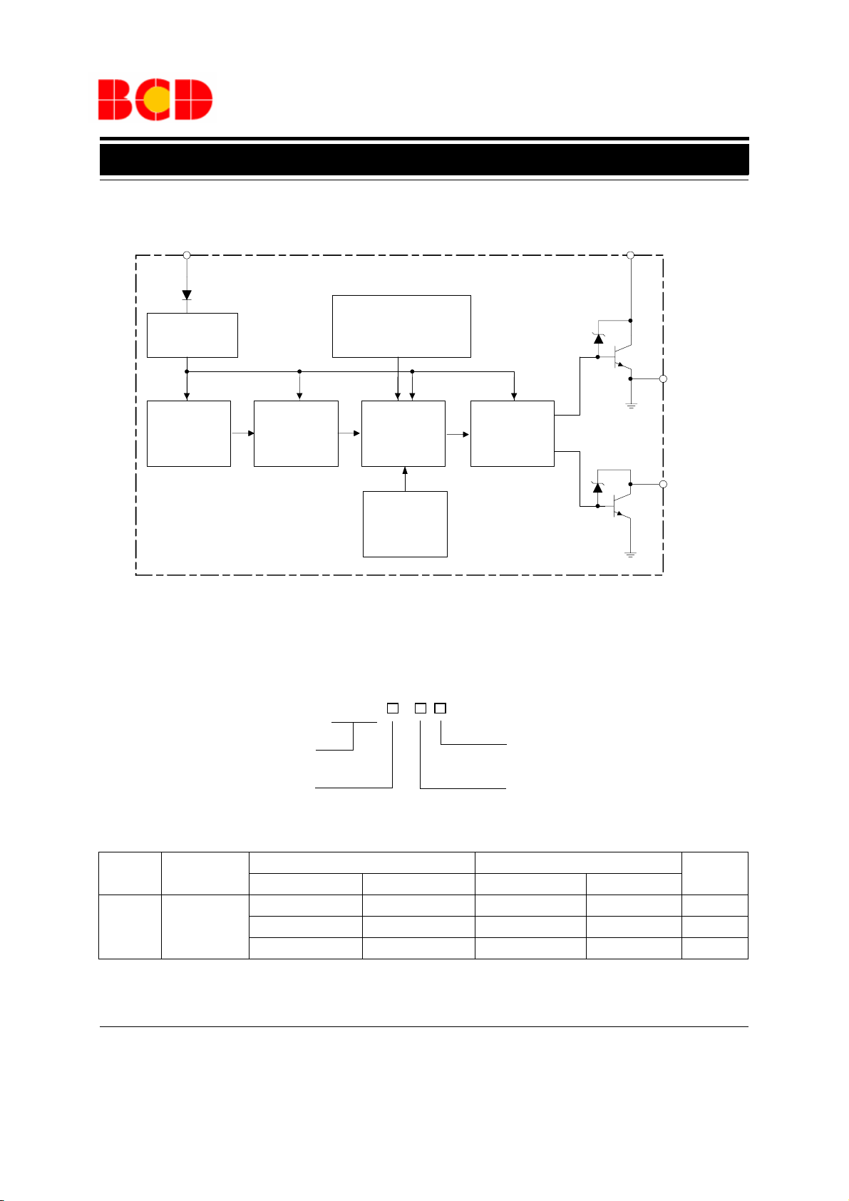
The AH276 is an integrated Hall sensor with output
driver designed for electronic commutation of brushless DC motor applications. The device includes an onchip Hall sensor for magnetic sensing, an amplifier
that amplifies the Hall voltage, a Schmitt trigger to
provide switching hysteresis for noise rejection, a temperature compensation circuit to compensate the temperature drift of Hall sensitivity and two
complementary open-collector drivers for sinking
large load current. It also includes an internal band-gap
regulator which is used to provide bias voltage for
internal circuits.
Placing the device in a variable magnetic field, if the
magnetic flux density is larger than threshold B
pin DO will be turned low (on) and pin DOB will be
turned high (off). This output state is held until the
magnetic flux density reverses and falls below B
then causes DO to be turned high (off) and DOB
turned low (on).
AH276 is available in TO-94 (SIP-4L) package.
OP
, the
RP,
Features
· On-Chip Hall Sensor
· 3.5V to 16V Supply Voltage
· 350mA (avg) Output Sink Current
· Reversed Supply Voltage Protection
· Build in Over Temperature Protection Function
o
· -20
· Low Profile TO-94 (SIP-4L) Package
· ESD Rating: 300V (Machine Model)
C to 85oC Operating Temperature
Applications
· Dual-Coil Brushless DC Motor
· Dual-Coil Brushless DC Fan
· Revolution Counting
· Speed Measurement
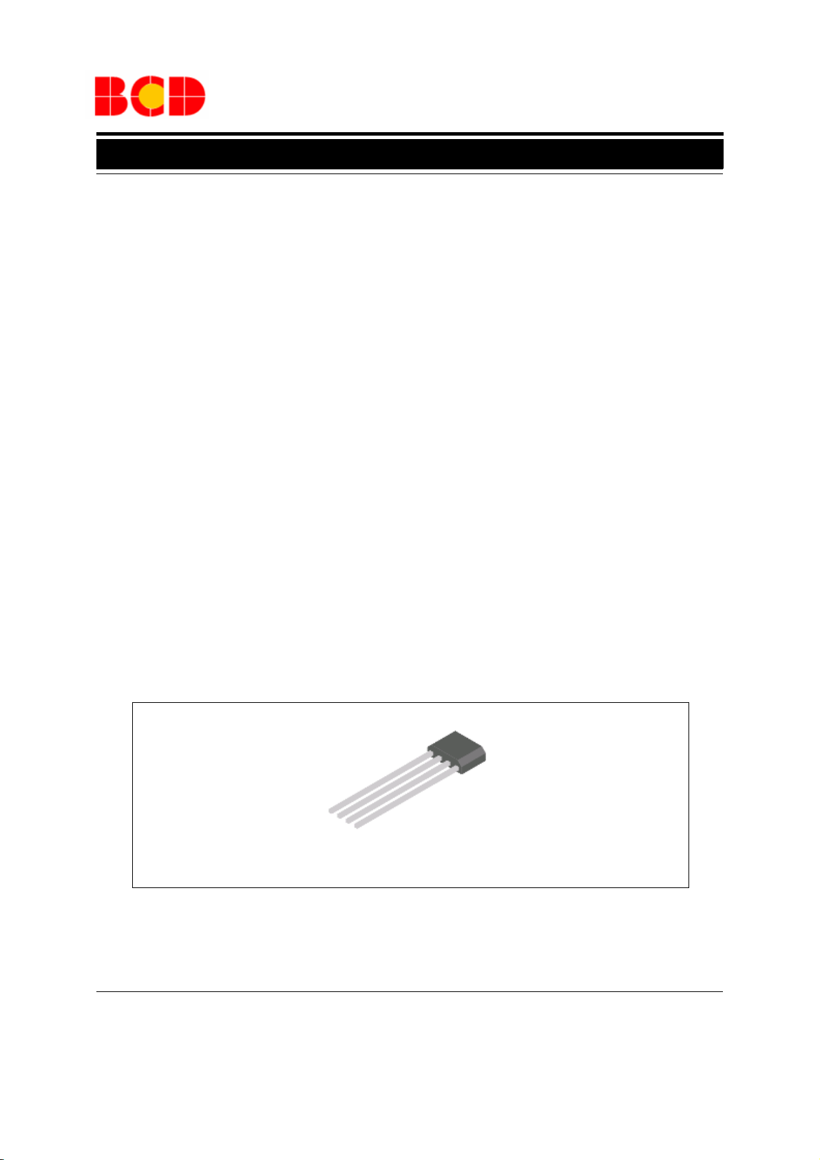
TO-94
Figure 1. Package Type of AH276
Nov. 2009 Rev. 1. 4 BCD Semiconductor Manufacturing Limited
1
Page 2
Data Sheet
COMPLEMENTARY OUTPUT HALL EFFECT LATCH AH276
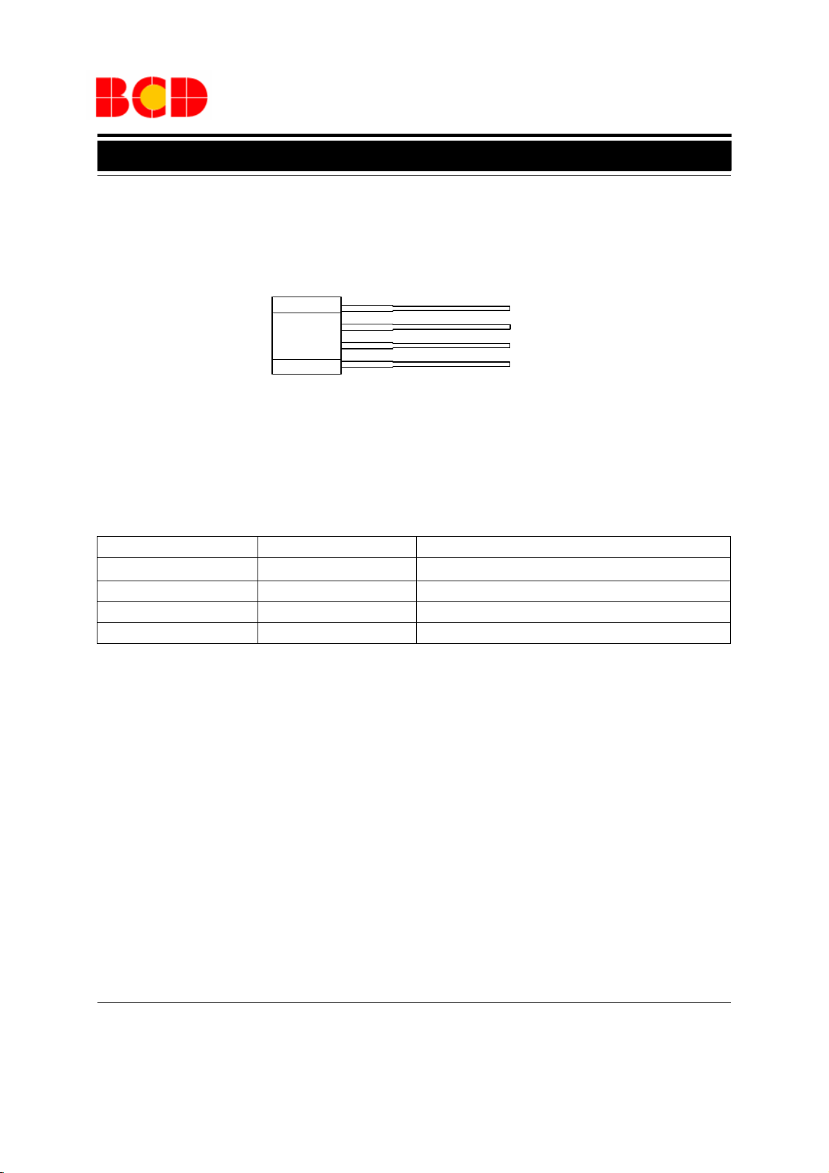
Pin Configuration
Z4 Package
(TO-94)
Pin Description
Pin Number Pin Name Function
1
2 DO Output 1
3 DOB Output 2
4 GND Ground
4
3
2
1
Figure 2. Pin Configuration of AH276 (Front View)
V
CC
Supply voltage
GND
DOB
DO
V
CC
Nov. 2009 Rev. 1. 4 BCD Semiconductor Manufacturing Limited
2
Page 3
Data Sheet
COMPLEMENTARY OUTPUT HALL EFFECT LATCH AH276
Functional Block Diagram
V
CC
1
Regulator
Temperature
Compensation
DO
2
4
GND
Hall
Sensor
Ordering Information
Circuit Type
Package
Z4: TO-94 (SIP-4L)
Amplifier
Figure 3. Functional Block Diagram of AH276
Schmitt
Trigger
Over
Temperature
Protection
Output
Driver
AH276 -
E1: Lead Free
G1: Green
Magnetic Characteristics
A: 10 to 50Gauss
B: 5 to 70Gauss
C: 100Gauss
3
DOB
Package
TO-94
BCD Semiconductor's Pb-free products, as designated with "E1" suffix in the part number, are RoHS compliant. Products with
"G1" suffix are available in green package.
Temperature
Range
o
-20 to 85
C
Lead Free Green Lead Free Green
AH276Z4-AE1 AH276Z4-AG1 AH276Z4-E1 AH276Z4-G1 Bulk
AH276Z4-BE1 AH276Z4-BG1 AH276Z4-E1 AH276Z4-G1 Bulk
AH276Z4-CE1 AH276Z4-CG1 AH276Z4-E1 AH276Z4-G1 Bulk
Part Number Marking ID
Packing
Typ e
Nov. 2009 Rev. 1. 4 BCD Semiconductor Manufacturing Limited
3
Page 4
Data Sheet
COMPLEMENTARY OUTPUT HALL EFFECT LATCH AH276
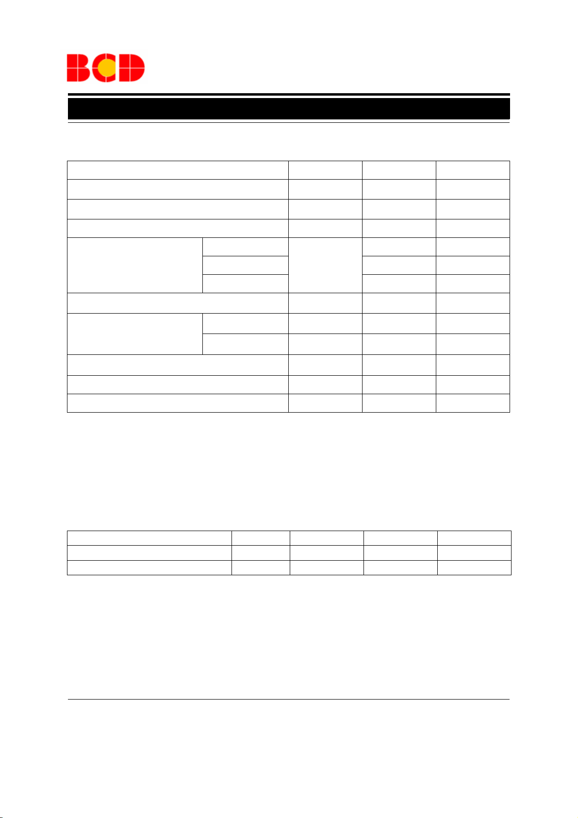
Absolute Maximum Ratings (Note 1)
(T
=25oC)
A
Parameter Symbol Value Unit
Supply Voltage V
Reverse Protection Voltage V
CC
RCC
20 V
-20 V
Magnetic Flux Density B Unlimited Gauss
Output Current
Continuous
Hold 550 mA
I
O
350 mA
Peak (start up) 750 mA
Power Dissipation P
Die to atmosphere θJA 227
D
550 mW
o
C/W
Thermal Resistance
Die to package case θJC 49
Storage Temperature T
STG
-50 to 150
o
C/W
o
C
ESD (Machine Model) 300 V
ESD (Human Body Model) 2500 V
Note 1: Stresses greater than those listed under "Absolute Maximum Ratings" may cause permanent damage to the device.
These are stress ratings only, and functional operation of the device at these or any other conditions beyond those indicated
under "Recommended Operating Conditions" is not implied. "Absolute Maximum Ratings" for extended period may affect
device reliability.
Recommended Operating Conditions
(TA=25oC)
Parameter Symbol Min Max Unit
Supply Voltage
Ambient Temperature
V
CC
T
A
Nov. 2009 Rev. 1. 4 BCD Semiconductor Manufacturing Limited
4
3.5 16 V
-20 85
o
C
Page 5
Data Sheet
COMPLEMENTARY OUTPUT HALL EFFECT LATCH AH276
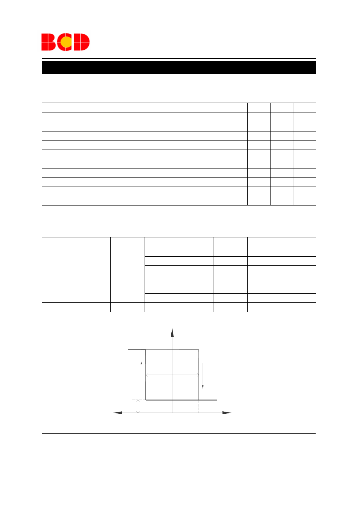
Electrical Characteristics
(TA=25oC, VCC=14V, unless otherwise specified)
Parameter Symbol Test Condition Min Typ Max Unit
Output Saturation Voltage
Output Leakage Current I
Supply Current I
V
OL
CC
Output Rise Time tr R
Output Fall Time tf R
Switch Time Differential ∆tR
Output Zener Breakdown Voltage V
Thermal Protection Temperature TSD 178
Thermal Protection Hysteresis ∆TSD 40
VCC=3.5V, IO=100mA 0.3 V
SAT
=350mA 0.35 0.6 V
I
O
VCE=16V 0.1 10 µA
VCC=16V, Output Open 12 16 mA
=820Ω, CL=20pF 3.0 10 µs
L
=820Ω, CL=20pF 0.3 1.5 µs
L
=820Ω, CL=20pF 3.0 10 µs
L
Z
55 V
o
C
o
C
Magnetic Characteristics
(TA=25oC)
Parameter Symbol Grade Min Typ Max Unit
A10 50Gauss
Operating Point
B
OP
B 5 70 Gauss
C 100 Gauss
A-50 -10Gauss
Releasing Point
B
RP
B -70 -5 Gauss
C -100 Gauss
Hysteresis B
High
Turn off Turn on
HYS
Off-state
V
SAT
VDO (V)
B
HYS
On-state
B
RP
Magnetic Flux Density (Gauss)
0
B
OP
75 Gauss
Low
SN
Nov. 2009 Rev. 1. 4 BCD Semiconductor Manufacturing Limited
5
Page 6
Data Sheet
COMPLEMENTARY OUTPUT HALL EFFECT LATCH AH276
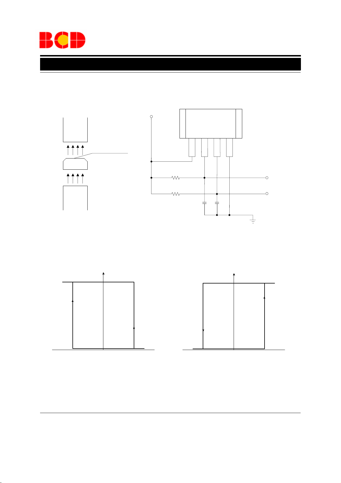
Magnetic Characteristics (Continued)
S
Marking Side
N
DO (V)
V
CC
-40 -20 0 20 40
Magnetic Flux Density B (Gauss)
16
14
12
10
8
6
4
2
+14V
V
CC
12
R1
820Ω
R2
820Ω
Figure 4. Basic Test Circuit
V
SAT
V
SAT
-40 -20 0 20 40
AH276
DO DOB GND
4
3
C1 C2
20pF 20pF
DOB (V)
16
14
12
10
8
6
4
2
Magnetic Flux Density B (Gauss)
DO (V
DOB (V
OUT1
OUT2
)
)
V
CC
Figure 5. V
vs. Magnetic Flux Density
DO
Figure 6. V
vs. Magnetic Flux Density
DOB
Nov. 2009 Rev. 1. 4 BCD Semiconductor Manufacturing Limited
6
Page 7
Data Sheet
COMPLEMENTARY OUTPUT HALL EFFECT LATCH AH276
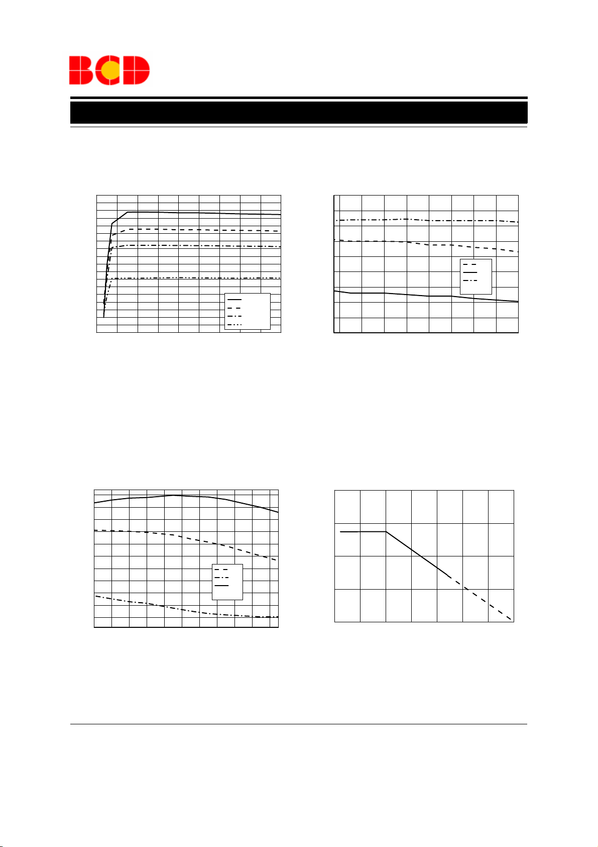
Typical Performance Characteristics
14
13
12
11
10
(mA)
9
CC
I
8
7
6
5
2 4 6 8 10 12 14 16 18 20
Ta=-25OC
Ta=-0OC
Ta=+25OC
Ta=+85OC
VCC (V)
Figure 7. I
CC
vs. V
CC
100
80
60
40
20
(Gauss)
HYS
0
/B
RP
/B
-20
OP
B
-40
-60
-80
4 6 8 101214161820
B
B
B
Ta=25OC
OP
RP
HYS
VCC (V)
Figure 8. B
OP/BRP/BHYS
vs. V
CC
75
50
25
(Gauss)
HYS
0
/B
RP
/B
OP
B
-25
-50
-20 0 20 40 60 80
Figure 9. BOP/BRP/B
TA (OC)
vs. Ambient Temperature
HYS
B
B
B
TA=+25OC
OP
RP
HYS
800
600
400
(mW)
D
P
200
0
-25 0 25 50 75 100 125 150
TA (oC)
Figure 10. PD vs. Ambient Temperature
Nov. 2009 Rev. 1. 4 BCD Semiconductor Manufacturing Limited
7
Page 8
Data Sheet
COMPLEMENTARY OUTPUT HALL EFFECT LATCH AH276
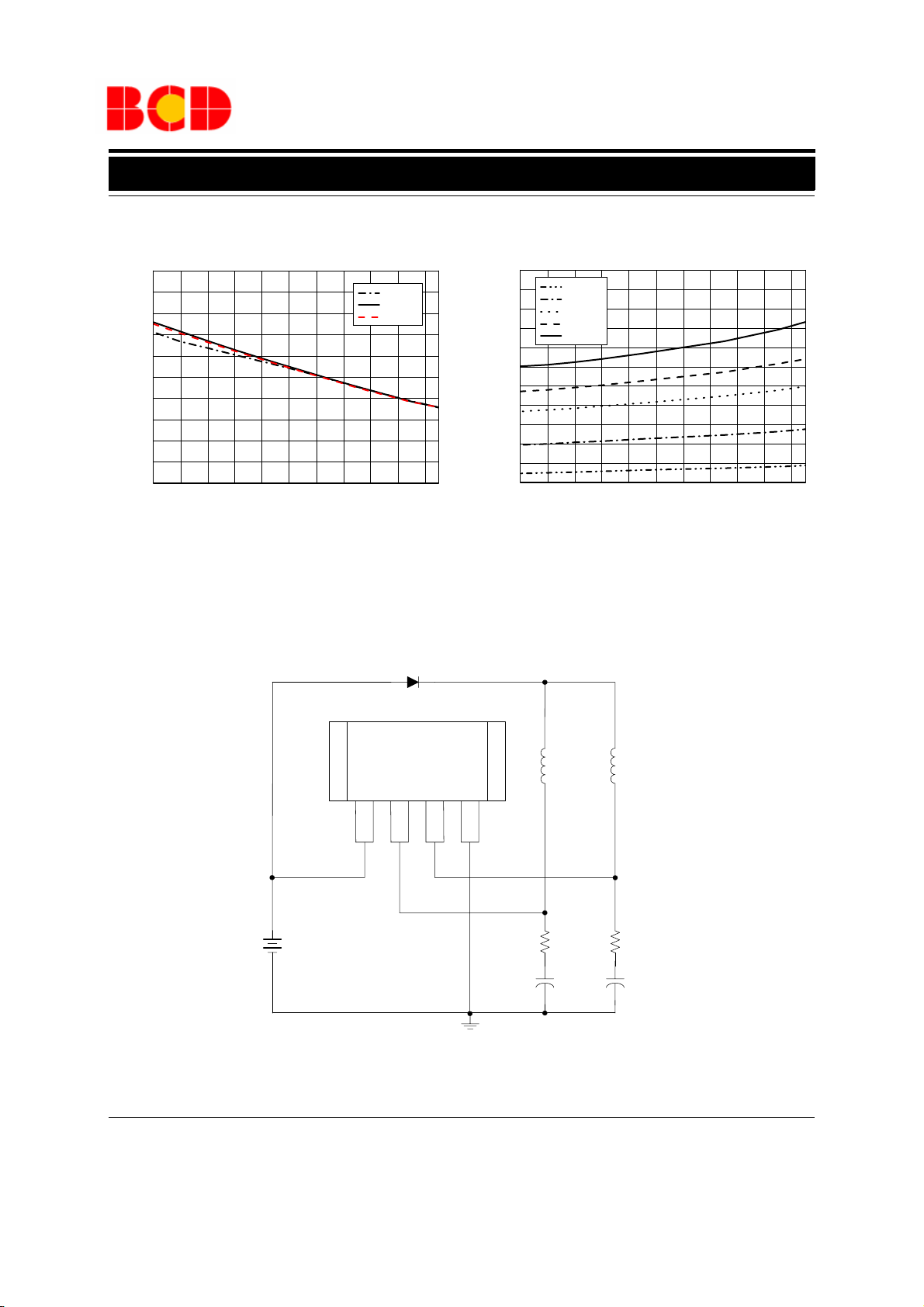
Typical Performance Characteristics (Continued)
14
12
10
(mA)
CC
I
8
6
-20 0 20 40 60 80
TA (OC)
Figure 11. ICC vs. Ambient Temperature
Typical Applications
VCC=3.5V
VCC=14V
VCC=20V
D1
600
5
IO=100mA
500
400
(mV)
300
SAT
V
200
100
-20 0 20 40 60 80
IO=200mA
IO=300mA
IO=350mA
IO=400mA
Figure 12. V
SAT
TA(OC)
vs. Ambient Temperature
AH276
COIL1 COIL2
V
CC
DO DOB GND
12
V
CC
4
3
R1
470
C1
2.2µF
++
R2
470
C2
2.2µF
Figure 12. Typical Application Circuit
Nov. 2009 Rev. 1. 4 BCD Semiconductor Manufacturing Limited
8
Page 9
Data Sheet
COMPLEMENTARY OUTPUT HALL EFFECT LATCH AH276
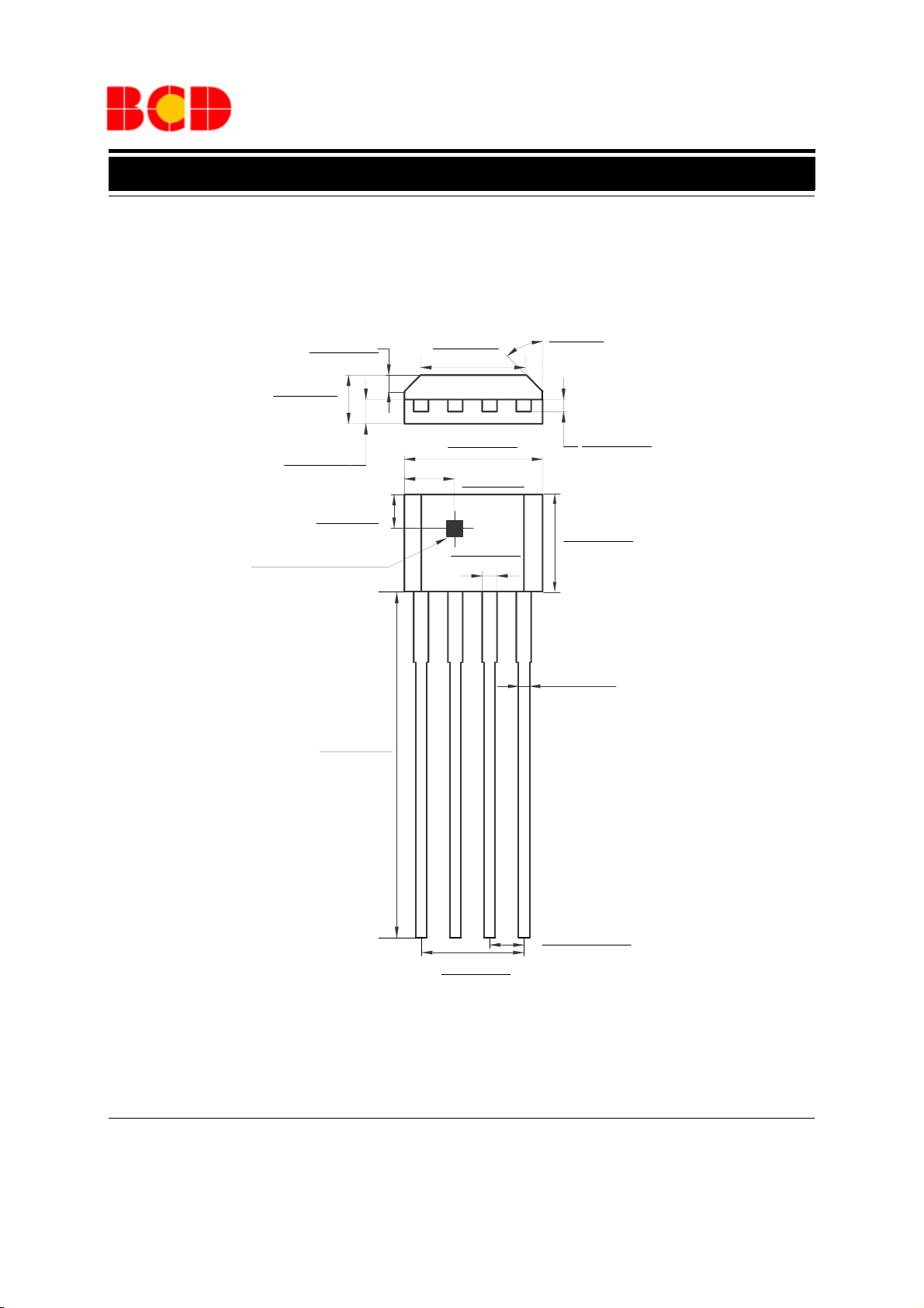
Mechanical Dimensions
Unit: mm(inch)TO-94
0.500(0.020)
0.700(0.028)
1.520(0.059)
1.720(0.067)
0.700(0.028)
0.900(0.035)
1.250(0.050)
Package Sensor Location
(For Hall IC)
14.000(0.550)
15.300(0.602)
0.149)
3.780(
4.080(
0.161)
4.980(0.196)
5.280(0.208)
1.850(0.073)
0.380(0.015)
0.550(0.022)
45 °TYP
0.360(0.014)
0.510(0.020)
3.450(0.136)
3.750(0.148)
0.360(0.014)
0.500(0.020)
1.270(0.050) TYP
3.710(0.146)
3.910(0.154)
Nov. 2009 Rev. 1. 4 BCD Semiconductor Manufacturing Limited
9
Page 10

BCD Semiconductor Manufacturing Limited
IMPORTANT NOTICE
IMPORTANT NOTICE
BCD Semiconductor Manufacturing Limited reserves the right to make changes without further notice to any products or specifi-
BCD Semiconductor Manufacturing Limited reserves the right to make changes without further notice to any products or specifi-
cations herein. BCD Semiconductor Manufacturing Limited does not assume any responsibility for use of any its products for any
cations herein. BCD Semiconductor Manufacturing Limited does not assume any responsibility for use of any its products for any
particular purpose, nor does BCD Semiconductor Manufacturing Limited assume any liability arising out of the application or use
particular purpose, nor does BCD Semiconductor Manufacturing Limited assume any liability arising out of the application or use
of any its products or circuits. BCD Semiconductor Manufacturing Limited does not convey any license under its patent rights or
of any its products or circuits. BCD Semiconductor Manufacturing Limited does not convey any license under its patent rights or
other rights nor the rights of others.
other rights nor the rights of others.
http://www.bcdsemi.com
MAIN SITE
MAIN SITE
- Headquarters
BCD Semiconductor Manufacturing Limited
BCD Semiconductor Manufactur ing Limited
- Wafer Fab
No. 1600, Zi Xing Road, Shanghai ZiZhu Science-based Industrial Park, 200241, China
Shanghai SIM-BCD Semiconductor Manufacturing Limited
Tel: +86-21-24162266, Fax: +86-21-24162277
800, Yi Shan Road, Shanghai 200233, China
Tel: +86-21-6485 1491, Fax: +86-21-5450 0008
REGIONAL SALES OFFICE
Shenzhen Office
REGIONAL SALES OFFICE
Shanghai SIM-BCD Semiconductor Manufacturing Co., Ltd., Shenzhen Office
Shenzhen Office
Unit A Room 1203, Skyworth Bldg., Gaoxin Ave.1.S., Nanshan District, Shenzhen,
Shanghai SIM-BCD Semiconductor Manufacturing Co., Ltd. Shenzhen Office
China
Advanced Analog Circuits (Shanghai) Corporation Shenzhen Office
Tel: +86-755-8826 7951
Room E, 5F, Noble Center, No.1006, 3rd Fuzhong Road, Futian District, Shenzhen 518026, China
Fax: +86-755-8826 7865
Tel: +86-755-8826 7951
Fax: +86-755-8826 7865
- Wafer Fab
BCD Semiconductor Manufacturing Limited
Shanghai SIM-BCD Semiconductor Manufacturing Co., Ltd.
- IC Design Group
800 Yi Shan Road, Shanghai 200233, China
Advanced Analog Circuits (Shanghai) Corporation
Tel: +86-21-6485 1491, Fax: +86-21-5450 0008
8F, Zone B, 900, Yi Shan Road, Shanghai 200233, China
Tel: +86-21-6495 9539, Fax: +86-21-6485 9673
Taiwan Office
BCD Semiconductor (Taiwan) Company Limited
Taiwan Office
4F, 298-1, Rui Guang Road, Nei-Hu District, Taipei,
BCD Semiconductor (Taiwan) Company Limited
Tai wan
4F, 298-1, Rui Guang Road, Nei-Hu District, Taipei,
Tel: +886-2-2656 2808
Taiwan
Fax: +886-2-2656 2806
Tel: +886-2-2656 2808
Fax: +886-2-2656 2806
USA Office
BCD Semiconductor Corp.
USA Office
30920 Huntwood Ave. Hayward,
BCD Semiconductor Corporation
CA 94544, USA
30920 Huntwood Ave. Hayward,
Tel : +1-510-324-2988
CA 94544, U.S.A
Fax: +1-510-324-2788
Tel : +1-510-324-2988
Fax: +1-510-324-2788
 Loading...