

Page 1
A
Green
Description
AH266 is an integrated Hall sensor with output drivers designed for
electronic commutation of brush-less DC motor applications. The
device includes an on-chip Hall voltage generator for magnetic
sensing, a comparator that amplifies the Hall voltage, a Schmitt
trigger to provide switching hysteresis for noise rejection, and
complementary Darlington open-collector drivers for sinking large
current loads. An internal band-gap regulator is used to provide
temperature compensated supply voltage for internal circuits and
allows a wide operating supply range.
If a magnetic flux density (B) is larger than operation point (Bop), DO
will turn on (low) and DOB will turn off (high). The output state is
latched prior to reaching release point (Brp). If B< Brp, DO will turn off
and DOB will turn on. AH266 is rated for operation over temperature
range from -20°C to +85°C
devices are available in low cost die forms or rugged 4 pin SIP
packages.
and voltage range from 4V to 28V. The
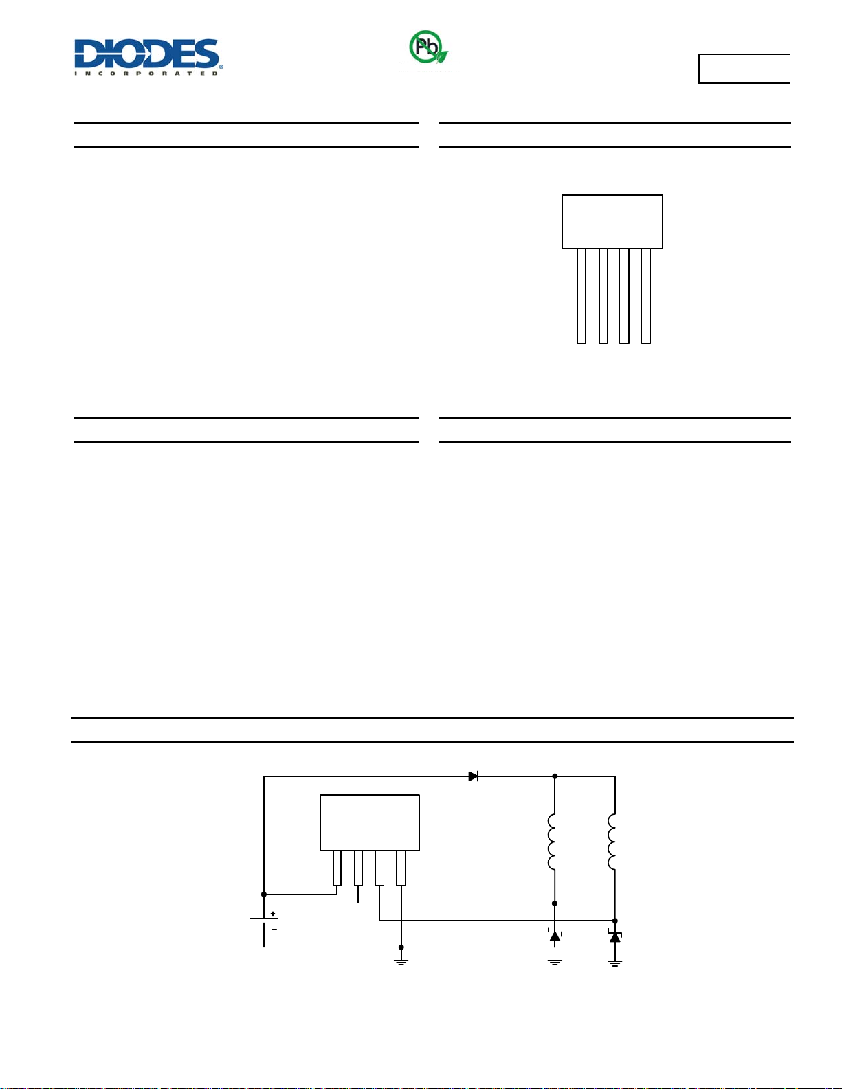
Pin Assignments
H266
HIGH VOLTAGE HALL EFFECT LATCH
( Top View )
266
1 243
SIP-4
Features
On-Chip Hall Plate
Operating Voltage: 4V to 28V
Output Current: 400mA (Continuous, +25°C)
Reverse Protection Diode Only for Chip Reverse Power
Connecting (Note 1)
Output Protection Zener Breakdown V
Lead Free package: SIP-4
SIP-4: Available in “Green” Molding Compound (No Br, Sb)
RoHS Compliant (Note 2)
Lead-Free Finish; RoHS Compliant (Notes 1 & 2)
Halogen and Antimony Free. “Green” Device (Note 3)
Notes: 1. EU Directive 2002/95/EC (RoHS) & 2011/65/EU (RoHS 2) compliant. All applicable RoHS exemptions applied.
2. See http://www.diodes.com/quality/lead_free.html for more information about Diodes Incorporated’s definitions of Halogen- and Antimony-free, "Green"
and Lead-free.
3. Halogen- and Antimony-free "Green” products are defined as those which contain <900ppm bromine, <900ppm chlorine (<1500ppm total Br + Cl) and
<1000ppm antimony compounds.
= 62V (Typ.)
Z
Applications
Dual-Coil Brushless DC Motor
Dual-Coil Brushless DC Fan
Revolution Counting
Speed Measurement
Typical Applications Circuit
266
Coil 1
Coil 2
AH266
Document number: DS30876 Rev. 5 - 2
V
cc
12 43
Brush-Less DC Fan
1 of 7
www.diodes.com
December 2013
© Diodes Incorporated
Page 2
A
Pin Descriptions
Pin Name P/I/O Pin # Description
V
DO O 2 Output Pin
DOB O 3 Output Pin
GND P 4 Ground
Functional Block Diagram
V
CC
1
CC
H266
P 1 Power Supply Input
DO
REG.
Hal
l
Plate
Amp
Absolute Maximum Ratings (@T
Symbol Parameter Rating Unit
VCC
V
out (off)
I
O (con)
I
O (hold)
I
O (peak)
B Magnetic Flux Density Unlimited Gauss
TST
PD
θJA
θJC
AH266
Document number: DS30876 Rev. 5 - 2
Supply Voltage 28 V
Output “OFF ” Voltage 28 V
Output “ON” Current
Storage Temperature Range -65 to +150 °C
Power Dissipation (Note 6)
Thermal Resistance Junction-to-Ambient (SIP-4) 227 °C/W
Thermal Resistance Junction-to-Case (SIP-4) 49 °C/W
= +25°C, unless otherwise specified.)
A
2 of 7
www.diodes.com
400 (Note 5) mA
DOB
500 mA
700 mA
550 mW
December 2013
© Diodes Incorporated
Page 3
A
)
H266
Recommended Operating Conditions (@T
Symbol Characteristic Conditions Min Max Unit
VCC
TA
Notes: 4. This application circuit can’t protect reverse coil current if power is connecting reverse.
5. I
6. See Performance Characteristics for other conditions.
7. Shall not exceed P
Electrical Characteristics (@T
Symbol Characteristic Conditions Min Typ. Max Unit
Supply Voltage Operating 4 28 V
Operating Ambient Temperature (Note 7) Operating -20 85 °C
is 150 mA at +85°C.
o (con)
and Safety Operation Area.
D
= +25°C, unless otherwise specified.)
A
= +25°C, unless otherwise specified.)
A
Vz
V
CE (SAT
I
CEX
ICC
tr Output Rise Time
tf Output Falling Time
t Switch Time Differential
Output Zener Breakdown Output Turn off 54 62 70 V
Output Saturation Voltage
Output Leakage Current
Supply Current
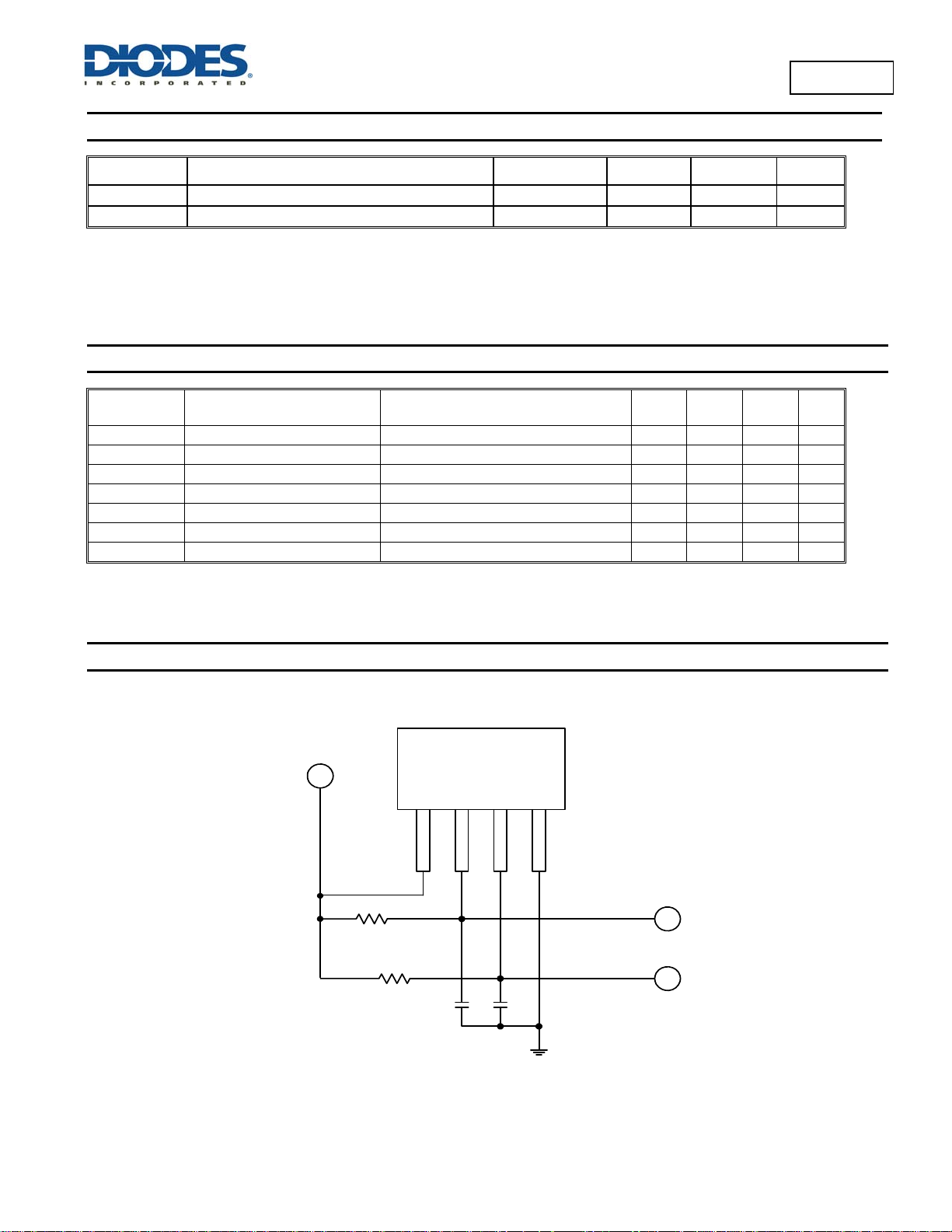
Test Circuit
24V
VCC = 24V, IC = 400mA
VCE = 24V, VCC = 24V
VCC = 24V, Output Open
V
= 24V, RL = 820Ω, CL = 20pF
CC
V
= 24V, RL = 820Ω, CL = 20pF
CC
V
= 24V, RL = 820Ω, CL = 20pF
CC
266
-
-
-
-
-
-
1.1 1.5 V
< 0.1
5 10 mA
1.0 5 µs
1.0 1.5 µs
3.0 10 µs
10 μA
V
1 (DO)
out
RL1
2 (DOB)
V
out
RL2
CL2
RL1 = RL2 = 820 Ohm
CL1 = CL2 = 20 pF
AH266
Document number: DS30876 Rev. 5 - 2
CL1
3 of 7
www.diodes.com
December 2013
© Diodes Incorporated
Page 4

A
H266
Magnetic Characteristics
A grade (1mT = 10 Gauss)
Symbol Characteristic Min Typ. Max Unit
Bop Operation Point 10 — 70 Gauss
Brp Release Point -70 — -10 Gauss
Bhy Hysteresis — 80 — Gauss
B grade
Symbol Characteristic Min Typ. Max Unit
Bop Operation Point — — 100 Gauss
Brp Release Point -100 — — Gauss
Bhy Hysteresis — 80 — Gauss
Output Voltage in Volts
Operation Characteristics
S
N
DOB
Marking Side
Output Voltage in Volts
V
SAT
High
(Output Voltage)
V
SAT
DO
Bhy Turn onTurn offBhy Turn offTurn on
V
SAT
BopBop BrpBrp
00
Magnetic Flux Density in GaussMagnetic Flux Density in Gauss
DO
V
CC
V
d
hy
B
Low
(SIP-4L)
AH266
Document number: DS30876 Rev. 5 - 2
N
B
0
rp
(Magnetic Flux Density )
4 of 7
www.diodes.com
B
op
S
December 2013
© Diodes Incorporated
Page 5

A
A
A
Performance Characteristics
T
(C)
PD (mW)
T
(C)
PD (mW)
(mW)
P
D
600
500
400
300
200
100
25 50 60 70 80 85 90 95 100
550 440 396 352 308 286 264 242 220
105 110 115 120
198 176 154 132
0
0 15 30 45 60 75 90 105 120 135 150
125 130 135 140 150
110 88 66 44 0
Power Dissipation Curve
85
H266
(°C)
T
A
Ordering Information
Device
AH266K-PG-B-A P SIP-4 1000 -B A
AH266K-PG-B-B P SIP-4 1000 -B B
Note: 8. For packaging details, go to our website at http://www.diodes.com/products/packages.html
Package
Code
Packaging
(Note 8)
Quantity Part Number Suffix
Bulk
Magnetic
Characteristics
Marking Information
( Top View )
Part Number
266X
Y WW X
X : Version : K
: Year : 0~9
Y
WW
: Week : 01~52, "52" represents
52 and 53 week
X : Internal Code : a~z : Lead Free
A~Z : Green
AH266
Document number: DS30876 Rev. 5 - 2
SIP-4L
www.diodes.com
5 of 7
December 2013
© Diodes Incorporated
Page 6

A
Package Outline Dimensions (All dimensions in mm.)
(1) Package type: SIP-4L
a
1︵2
x
︶
A
S
a
2︵2
x
︶
b
E
J
D
2
L
1
L
F
c
b
1
e
1
H266
Dim Min Max Typ
A 1.45 1.65 1.55
b1 0.38 0.44 0.40
b2 - - 0.48
c 0.35 0.45 0.40
x
︶
2
°
︵
5
4
x
3
.
0
D 5.12 5.32 5.22
e1 1.24 1.30 1.27
E 3.55 3.75 3.65
F 0.00 0.20 -
J 4.10 4.30 4.20
L 14.00 14.60 14.30
L1 1.32 1.52 1.42
S 0.63 0.83 0.73
a
4︵2
a
3︵2
x
︶
x
︶
a1 - 5° 3°
a2 4° 7° 5°
a3 4° 7° 5°
a4 - 5° 3°
All Dimensions in mm
SIP-4
AH266
Document number: DS30876 Rev. 5 - 2
6 of 7
www.diodes.com
December 2013
© Diodes Incorporated
Page 7

A
H266
DIODES INCORPORATED MAKES NO WARRANTY OF ANY KIND, EXPRESS OR IMPLIED, WITH REGARDS TO THIS DOCUMENT,
INCLUDING, BUT NOT LIMITED TO, THE IMPLIED WARRANTIES OF MERCHANTABILITY AND FITNESS FOR A PARTICULAR PURPOSE
(AND THEIR EQUIVALENTS UNDER THE LAWS OF ANY JURISDICTION).
Diodes Incorporated and its subsidiaries reserve the right to make modifications, enhancements, improvements, corrections or other changes
without further notice to this document and any product described herein. Diodes Incorporated does not assume any liability arising out of the
application or use of this document or any product described herein; neither does Diodes Incorporated convey any license under its patent or
trademark rights, nor the rights of others. Any Customer or user of this document or products described herein in such applications shall assume
all risks of such use and will agree to hold Diodes Incorporated and all the companies whose products are represented on Diodes Incorporated
website, harmless against all damages.
Diodes Incorporated does not warrant or accept any liability whatsoever in respect of any products purchased through unauthorized sales channel.
Should Customers purchase or use Diodes Incorporated products for any unintended or unauthorized application, Customers shall indemnify and
hold Diodes Incorporated and its representatives harmless against all claims, damages, expenses, and attorney fees arising out of, directly or
indirectly, any claim of personal injury or death associated with such unintended or unauthorized application.
Products described herein may be covered by one or more United States, international or foreign patents pending. Product names and markings
noted herein may also be covered by one or more United States, international or foreign trademarks.
This document is written in English but may be translated into multiple languages for reference. Only the English version of this document is the
final and determinative format released by Diodes Incorporated.
Diodes Incorporated products are specifically not authorized for use as critical components in life support devices or systems without the express
written approval of the Chief Executive Officer of Diodes Incorporated. As used herein:
A. Life support devices or systems are devices or systems which:
1. are intended to implant into the body, or
2. support or sustain life and whose failure to perform when properly used in accordance with instructions for use provided in the
labeling can be reasonably expected to result in significant injury to the user.
B. A critical component is any component in a life support device or system whose failure to perform can be reasonably expected to cause the
failure of the life support device or to affect its safety or effectiveness.
Customers represent that they have all necessary expertise in the safety and regulatory ramifications of their life support devices or systems, and
acknowledge and agree that they are solely responsible for all legal, regulatory and safety-related requirements concerning their products and any
use of Diodes Incorporated products in such safety-critical, life support devices or systems, notwithstanding any devices- or systems-related
information or support that may be provided by Diodes Incorporated. Further, Customers must fully indemnify Diodes Incorporated and its
representatives against any damages arising out of the use of Diodes Incorporated products in such safety-critical, life support devices or systems.
Copyright © 2013, Diodes Incorporated
www.diodes.com
IMPORTANT NOTICE
LIFE SUPPORT
AH266
Document number: DS30876 Rev. 5 - 2
7 of 7
www.diodes.com
December 2013
© Diodes Incorporated
 Loading...