

Page 1
A
Description
The AH1893 is a high sensitivity micropower Omnipolar Hall effect
switch IC with internal pull up and pull down capability. Designed for
portable and battery powered equipment such as cellular phones and
portable PCs to home appliances and industrial applications, the
average supply current is only 4.3µA at 1.85V. To support potable
equipment the AH1893 can operate over the supply range of 1.6V to
3.6V and uses a hibernating clocking system to minimize the power
consumption. To minimize PCB space the AH1893 is available in
small low profile X1-DFN1216-4 and SOT553 packages.
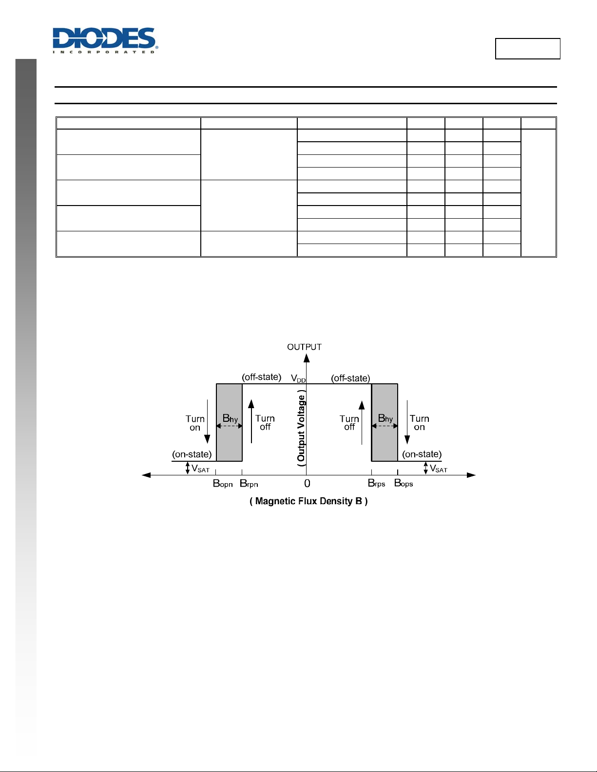
The output is activated with either a north or south pole of sufficient
magnetic field strength. When the magnetic flux density (B)
perpendicular to the package is larger than operate point (Bop), the
output will be turned on (pulled low) and held until B is lower than
release point (Brp).
Features
NEW PRODUCT
Omnipolar Operation (North or South pole)
Supply Voltage of 1.6V to 3.6V
High Sensitivity
Micropower Operation
Chopper Stabilized Design Provides
Superior Temperature Stability
Minimal Switch Point Drift
Enhanced Immunity to Physical Stress
No External Pull-up Resistors Required
Good RF Noise Immunity
-40°C to +85°C Operating Temperature
High ESD capability of 8kV (Human Body Model)
Small Low Profile SOT553 and X1-DFN1216-4 Packages
Totally Lead-Free & Fully RoHS Compliant (Notes 1 & 2)
Halogen and Antimony Free. “Green” Device (Note 3)
HIGH SENSITIVITY MICROPOWER
OMNIPOLAR HALL-EFFECT SWITCH
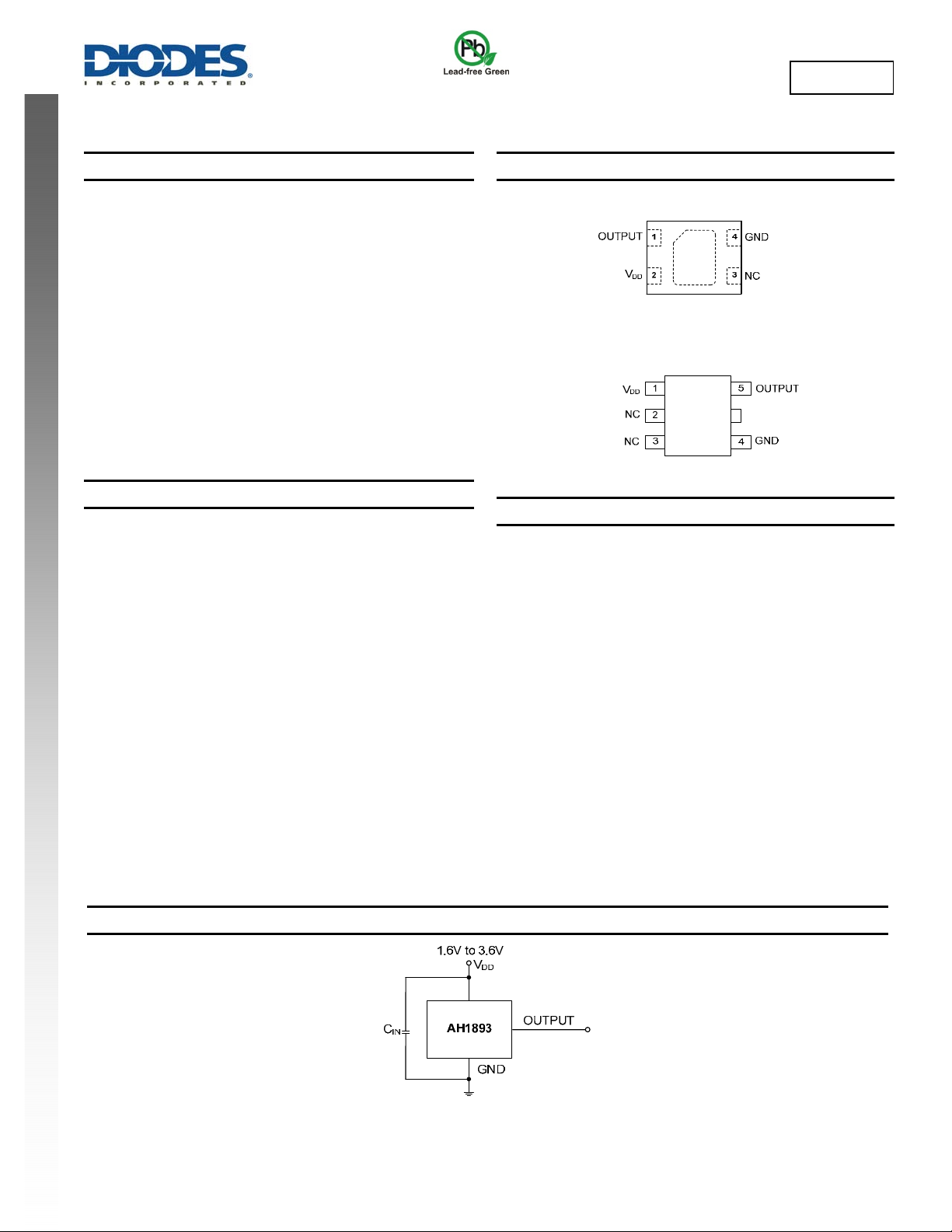
Pin Assignments
(Top View)
X1-DFN1216-4
(Top View)
SOT553
Applications
Open and Close Detect for Cellular Phones
Holster or Cover Detect for Cellular Phones and Tablet PCs
Cover or Display Switch in Portable PCs
Digital Still, Video Cameras and Handheld Gaming Consoles
Door, Lids and Tray Position Switches
Level, Proximity and Position Switches
Contact-Less Switches in Home Appliances and Industrial
Applications
H1893
Notes: 1. No purposely added lead. Fully EU Directive 2002/95/EC (RoHS) & 2011/65/EU (RoHS 2) compliant.
2. See http://www.diodes.com/quality/lead_free.html for more information about Diodes Incorporated’s definitions of Halogen- and Antimony-free, "Green"
and Lead-free.
3. Halogen- and Antimony-free "Green” products are defined as those which contain <900ppm bromine, <900ppm chlorine (<1500ppm total Br + Cl) and
<1000ppm antimony compounds.
Typical Applications Circuit
Note: 4. C
AH1893
Document number: DS35740 Rev. 1 - 2
is for power stabilization and to strengthen the noise immunity, the recommended capacitance is 100nF typical.
IN
www.diodes.com
1 of 10
July 2013
© Diodes Incorporated
Page 2
A
Pin Descriptions
Package: X1-DFN1216-4
Pin Number Pin Name Function
1 OUTPUT Output Pin
2
3 NC No Connection (Note 5)
4 GND Ground Pin
Package: SOT553
Pin Number Pin Name Function
1
2 NC No Connection (Note 5)
3 NC No Connection (Note 5)
4 GND Ground
5 OUTPUT Output
Note: 5. NC is “No Connection” pin and is not connected internally. This pin can be left open or tied to ground.
NEW PRODUCT
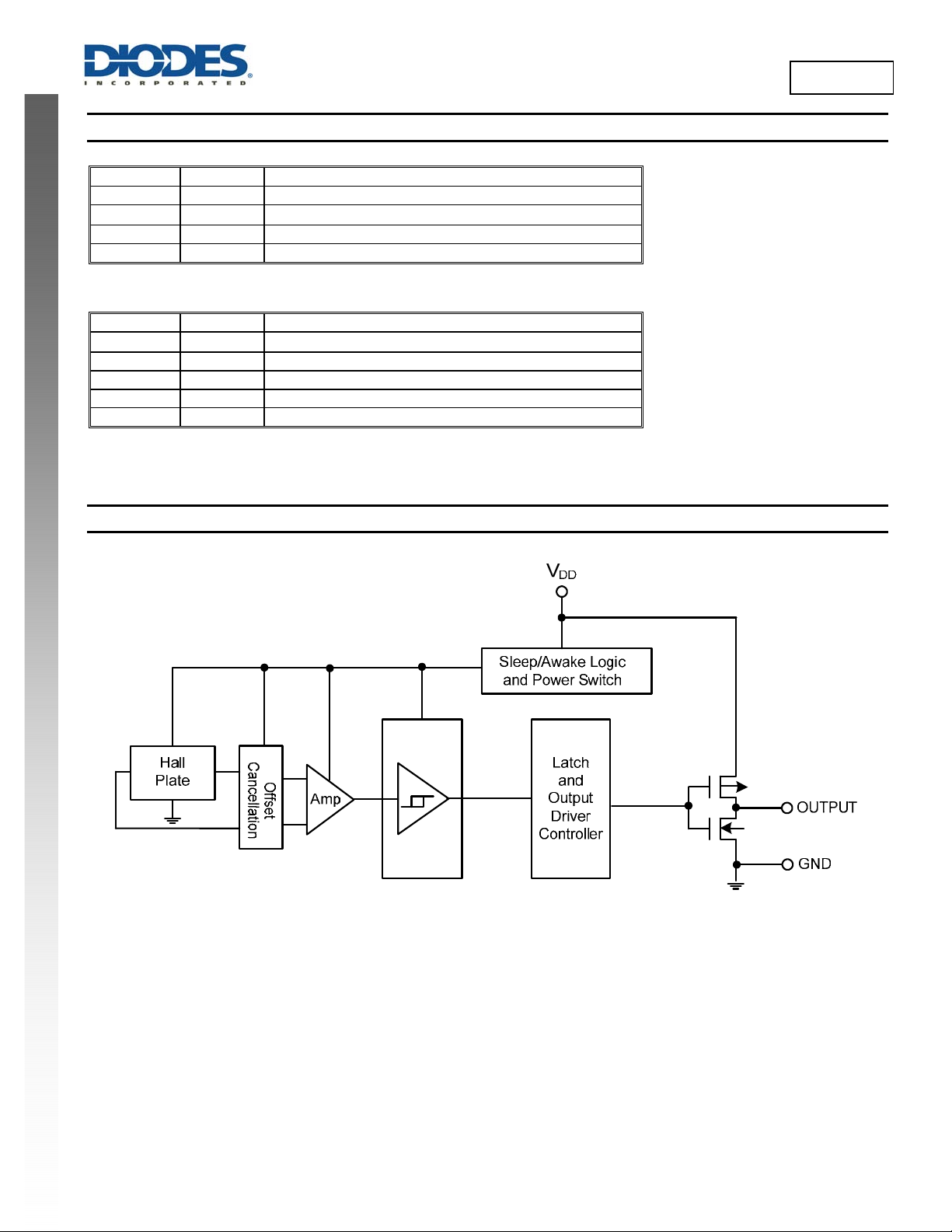
Functional Block Diagram
V
DD
V
DD
Power Supply Input
Power Supply Input
H1893
AH1893
Document number: DS35740 Rev. 1 - 2
2 of 10
www.diodes.com
July 2013
© Diodes Incorporated
Page 3
A
H1893
Absolute Maximum Ratings (Note 6) (@T
Symbol Parameter Rating Unit
VDD
V
DD_REV
I
OUTPUT
B Magnetic Flux Density Unlimited
PD
Ts Storage Temperature Range -65 to +150 °C
TJ
ESD HBM Human Body Model (HMB) ESD capability 8 kV
Notes: 6. Stresses greater than the 'Absolute Maximum Ratings' specified above may cause permanent damage to the device. These are stress ratings only;
functional operation of the device at these or any other conditions exceeding those indicated in this specification is not implied. Device reliability may be
affected by exposure to absolute maximum rating conditions for extended periods of time.
7. The absolute maximum V
operate the device at the absolute maximum rated conditions for any period of time.
Supply Voltage (Note 7) 6 V
Reverse Supply Voltage -0.3 V
Output current (source and sink) 3 mA
Package Power Dissipation
Maximum Junction Temperature 150 °C
of 6V is a transient stress rating and is not meant as a functional operating condition. It is not recommended to
DD
Recommended Operating Conditions (@T
NEW PRODUCT
Symbol Parameter Conditions Rating Unit
VDD
TA
Electrical Characteristics (@T
Symbol Parameter Conditions Min Typ Max Unit
VOL Output Lo w Voltage (on) I
VOH Output High Voltage (off) I
Ioff Output Leakage Current V
IDD(awake)
IDD(sleep)
IDD(avg)
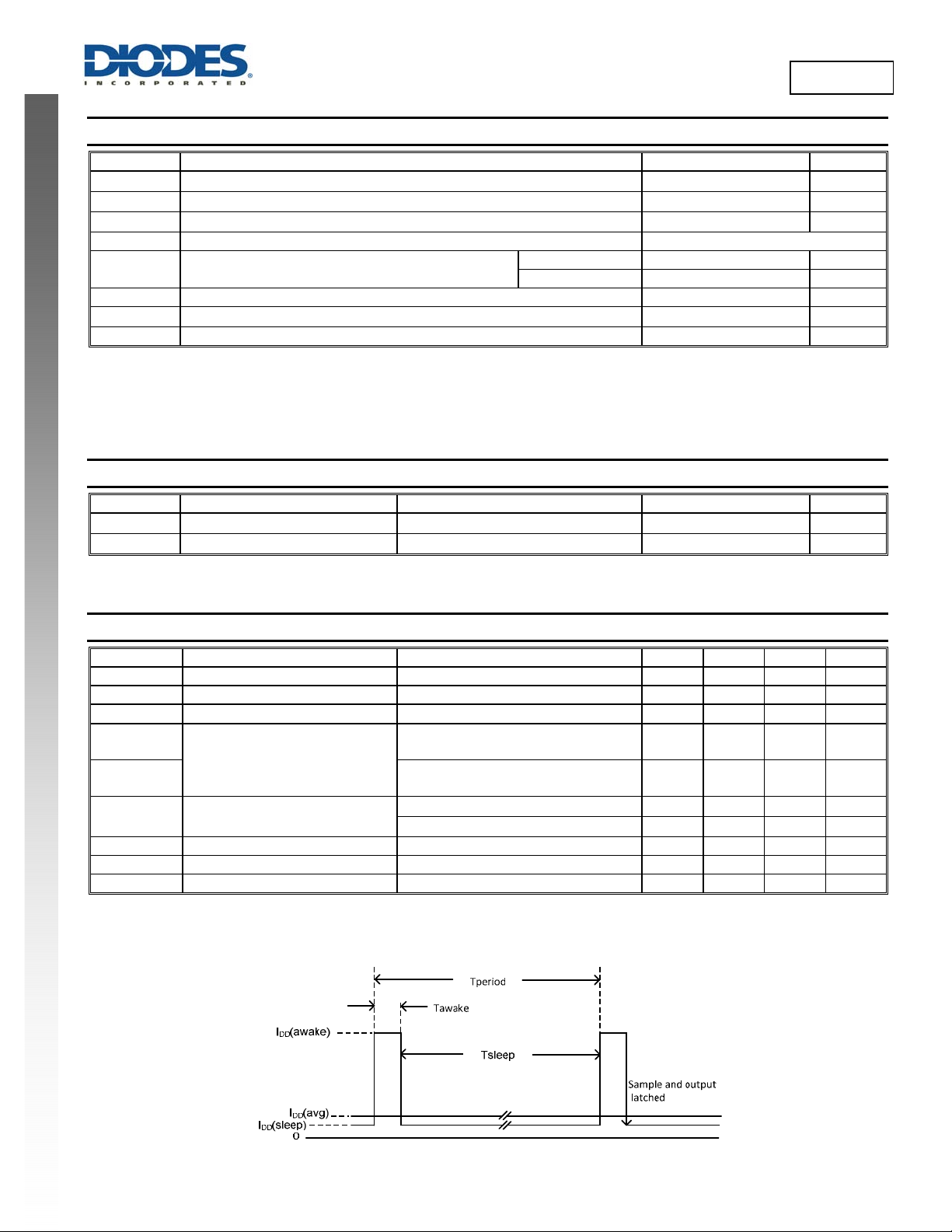
Tawake Awake Time (Note 8) — 50 100 µs
Tperiod Period (Note 8) — 50 100 ms
D.C. Duty Cycle — 0.1 — %
Note: 8. When power is initially turned on, the operating VDD (1.6V to 3.6V) must be applied to guaranteed the output sampling.
The output state is valid after the second operating cycle (typical 100ms).
Supply Voltage Operating 1.6V to 3.6V V
Operating Temperature Range Operating -40 to +85
= +25°C, VDD = 1.85V, unless otherwise specified.)
A
Supply Current
Average Supply Current
= +25°C, unless otherwise specified.)
A
X1-DFN1216-4 230 mW
SOT553 230 mW
= +25°C, unless otherwise specified.)
A
= 1mA - 0.1 0.2 V
OUT
= -1mA VDD-0.2 VDD-0.1 — V
OUT
= 3.6V, Output IOff — < 0.1 1 µA
OUT
During ‘Awake’ Period,
T
= +25°C, VDD = 3V
A
During ‘Sleep’ Period,
= +25°C, VDD = 3V
T
A
= +25°C, VDD = 1.85V
T
A
TA = +25°C, VDD = 3.6V
—
2.1 — mA
—
2.5 — mA
4.3 8 µA
—
7.2 13 µA
—
C
AH1893
Document number: DS35740 Rev. 1 - 2
3 of 10
www.diodes.com
July 2013
© Diodes Incorporated
Page 4
A
H1893
Magnetic Characteristics (Note 9 &10) (T
Symbol Characteristics Test Condition Min Typ Max Unit
Bops (south pole to part marking side)
Operation Point
Bopn (north pole to part marking side)
Brps (south pole to part marking side)
Brpn (north pole to part marking side)
Bhy (|Bopx|-|Brpx|) Hysteresis (Note 11)
Notes: 9. Typical data is at TA = +25C, VDD = 1.85V.
10. Maximum and minimum parameters values over the operating temperature range are not tested in production, they are guaranteed by design, process
control and characterization. The magnetic characteristics may vary with supply voltage, operating temperature and after soldering.
11. Maximum and minimum hysteresis is guaranteed by design and characterization.
NEW PRODUCT
= +25°C, VDD = 1.85V, unless otherwise specified)
A
T
= +25C
A
TA = -40°C to +85C
T
= +25C
A
TA = -40°C to +85C
T
= +25C
A
Release Point
TA = -40°C to +85C
= +25C
T
A
TA = -40°C to +85C
T
= +25C
A
TA = -40°C to +85C
(1mT=10 Gauss)
16 30 42
14 30 46
-42 -30 -16
-46 -30 -14
10 20 35
9 20 39
-35 -20 -10
-39 -20 -9
5 10 15
- 10 -
Gauss
AH1893
Document number: DS35740 Rev. 1 - 2
4 of 10
www.diodes.com
© Diodes Incorporated
July 2013
Page 5
A
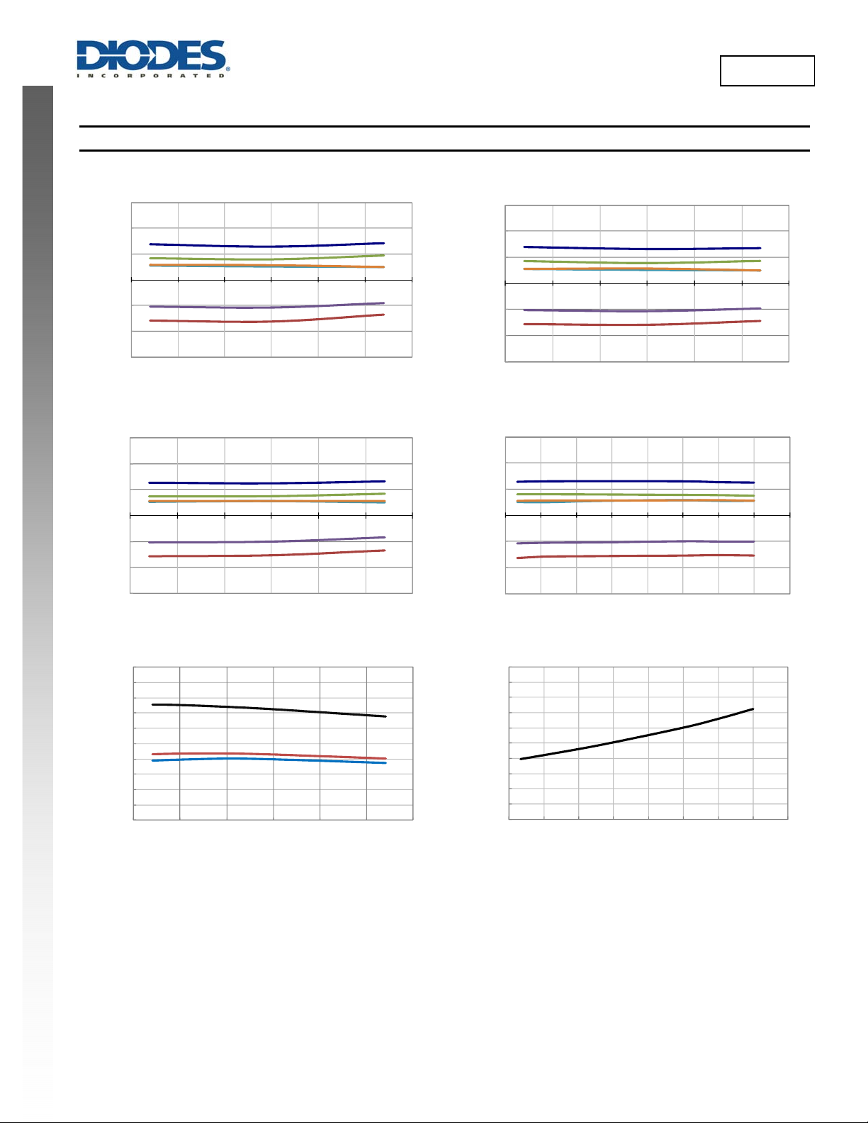
Typical Operating Characteristics
60
V
= 1.6V
DD
40
20
0
Gauss (G)
-20
-40
-60
-50-250 255075100
Temperature (°C)
Swit ch Poi nts vs Temperat ure
Bops
Brps
Bhy
Brpn
Bopn
H1893
60
= 1.85V
V
DD
40
20
0
-20
Gauss (G)
-40
-60
-50-250 255075100
Temperature (° C)
Switch Points vs Temperature
Bops
Brps
Bhy
Brpn
Bopn
NEW PRODUCT
60
VDD= 3.6V
40
20
0
Gau ss (G)
-20
-40
-60
-50 -25 0 25 50 75 100
Bops
Brps
Bhy
Brpn
Bopn
Temperature (° C)
Switch Points vs Temperature
10
9
(μA)
DD
8
7
6
5
4
3
2
1
0
Average Supply Current I
-50-25 0 255075100
3.6V
1.85V
1.6V
60
= +25°C
T
A
40
20
0
Gauss (G)
-20
-40
-60
1.5 1.8 2.1 2.4 2.7 3 3.3 3.6 3.9
Supply Voltage (V)
Swit ch Point s vs Suppl y Vo lt age
10
TA= +25°C
9
(μA)
8
DD
7
6
5
4
3
2
1
Average Supply Current I
0
1.5 1.8 2.1 2.4 2.7 3 3.3 3.6 3.9
Bops
Brps
Bhy
Brpn
Bopn
Temperature (°C)
A ver age Supply Current vs. Temperature
AH1893
Document number: DS35740 Rev. 1 - 2
5 of 10
www.diodes.com
Supply Voltage (V)
A ve r age Supply Curr ent vs. Supply Vol tage
© Diodes Incorporated
July 2013
Page 6
A
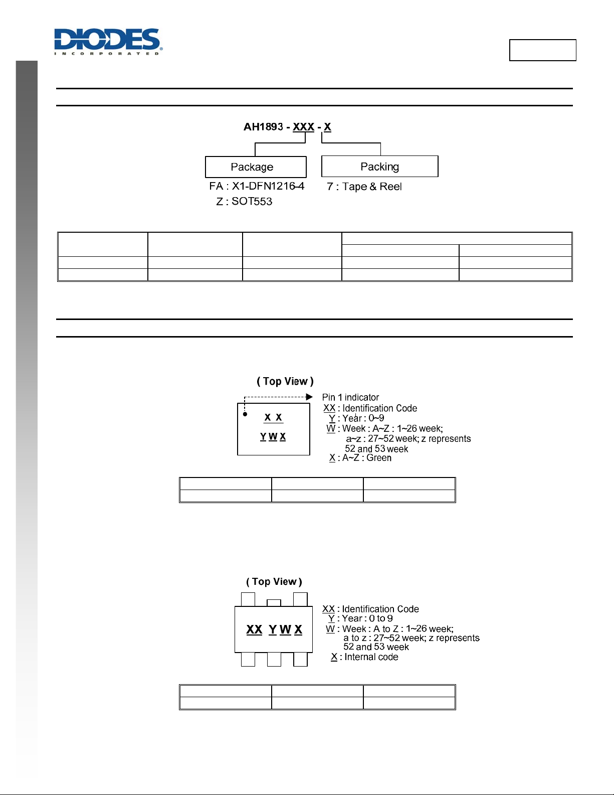
Ordering Information
H1893
Part Number
AH1893-FA-7 FA X1-DFN1216-4 3000/Tape & Reel -7
AH1893-Z-7 Z SOT553 3000/Tape & Reel -7
Marking Information
NEW PRODUCT
(1) Package Type: X1-DFN1216-4
(2) Package Type: SOT553
Package
Code
Part Number Package Identification Code
AH1893-FA-7 X1-DFN1216-4 B3
Packaging
Quantity Part Number Suffix
7” Tape and Reel
AH1893
Document number: DS35740 Rev. 1 - 2
Part Number Package Identification Code
AH1893-Z-7 SOT553 B3
6 of 10
www.diodes.com
July 2013
© Diodes Incorporated
Page 7
A
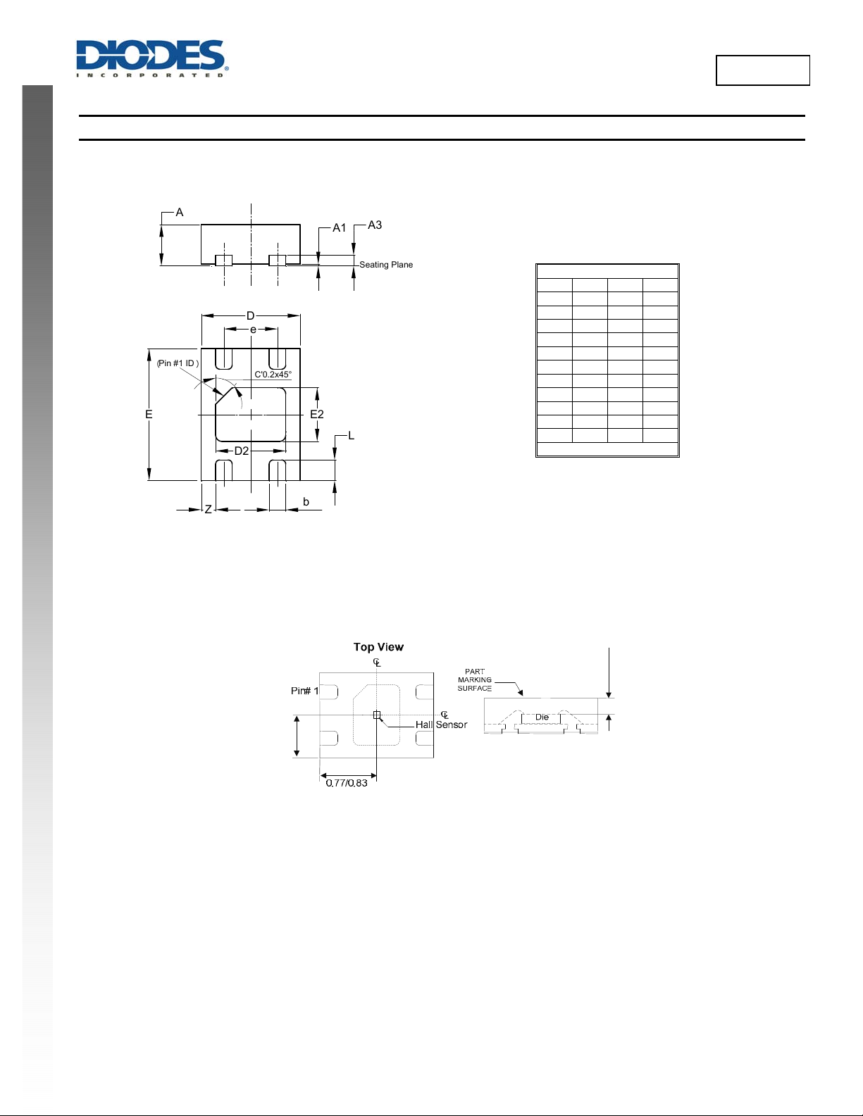
Package Outline Dimensions (All dimensions in mm.)
Please see AP02002 at http://www.diodes.com/datasheets/ap02002.pdf for latest version.
(1) Package Type: X1-DFN1216-4
A
A
A
3
1
Seating Plane
2
L
NEW PRODUCT
D
e
Pin #1 ID
︵
E
︶
Z
C'0.2x45°
D
2
Bottom View
E
b
H1893
X1-DFN1216-4
Dim Min Max Typ
A 0.47 0.53 0.50
A1 0.00 0.05 0.02
A3 -- -- 0.13
b 0.15 0.25 0.20
D 1.15 1.25 1.20
D2 0.75 0.95 0.85
E 1.55 1.65 1.60
E2 0.55 0.75 0.65
e - - 0.65
L 0.20 0.30 0.25
Z - - 0.175
All Dimensions in mm
0.57/0.63
AH1893
Document number: DS35740 Rev. 1 - 2
Sensor Location
7 of 10
www.diodes.com
0.11/0.25
July 2013
© Diodes Incorporated
Page 8
A
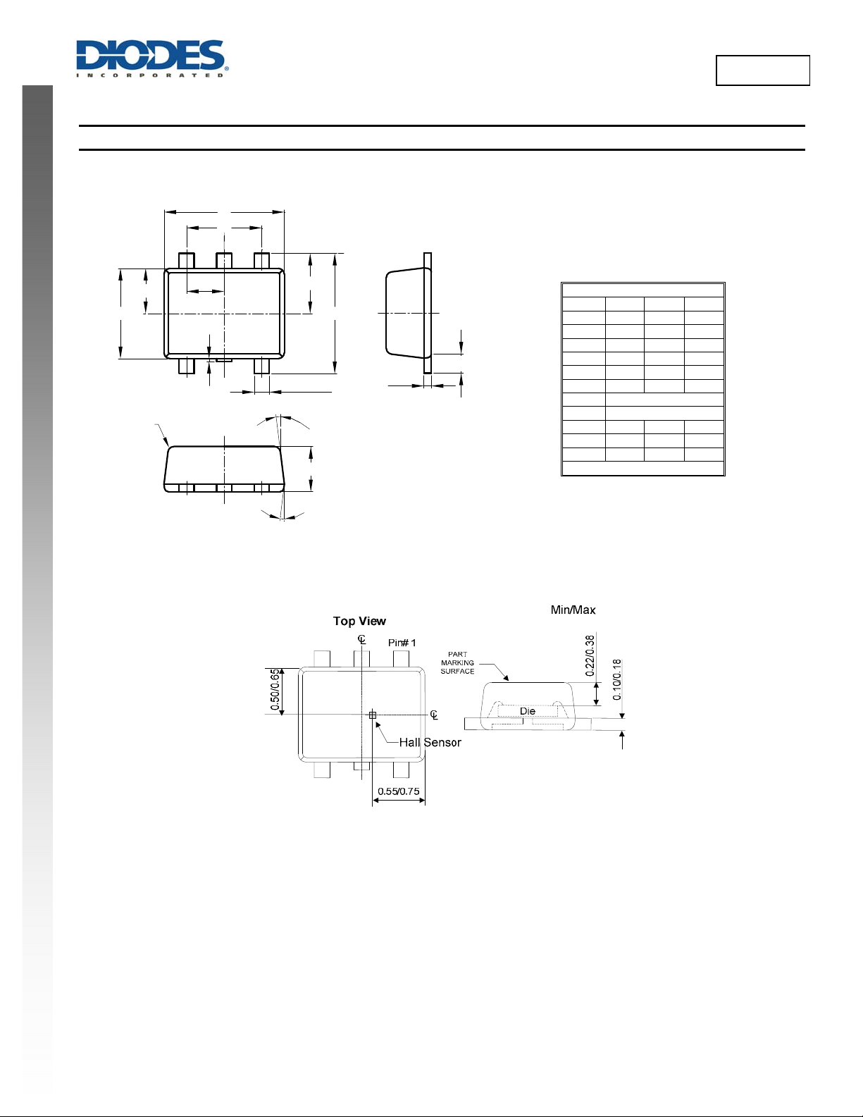
Package Outline Dimensions (cont.) (All dimensions in mm.)
(2) Package Type: SOT553
D
e1
E1/2
E1
e
E/2
E
NEW PRODUCT
R0.1 MAX.
TYP.
F
b (5x)
a
A
°
7
TYP.
c
L (5x)
H1893
SOT553
Dim Min Max Typ
A 0.55 0.62 0.60
b 0.15 0.30 0.20
c 0.10 0.18 0.15
D 1.50 1.70 1.60
E 1.55 1.70 1.60
E1 1.10 1.25 1.20
e 0.50 BSC
e1 1.00 BSC
F 0.00 0.10 ––
L 0.10 0.30 0.20
a 6° 8° 7°
All Dimensions in mm
AH1893
Document number: DS35740 Rev. 1 - 2
Sensor Location
8 of 10
www.diodes.com
July 2013
© Diodes Incorporated
Page 9
A
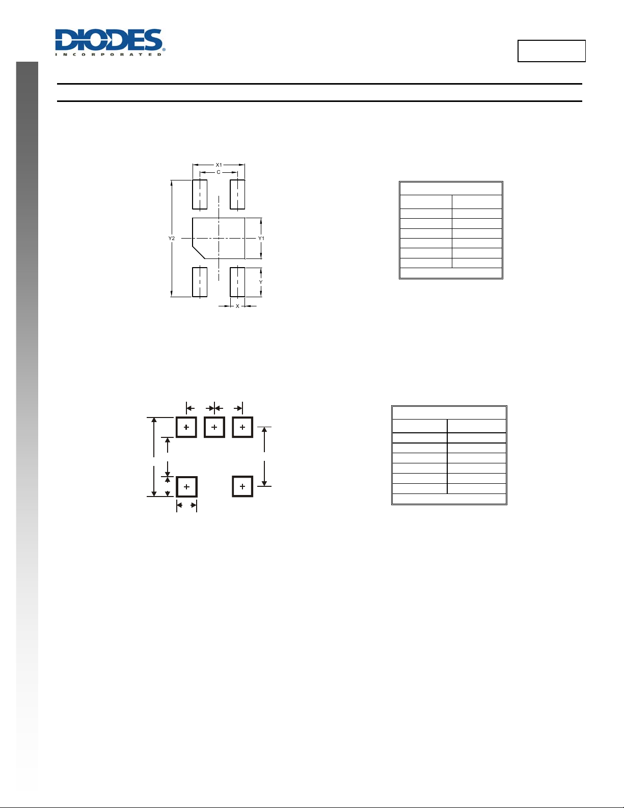
Suggested Pad Layout
Please see AP02001 at http://www.diodes.com/datasheets/ap02001.pdf for the latest version.
(1) Package Type: X1-DFN1216-4
X
1
C
Y
2
Y
1
Y
X
NEW PRODUCT
(2) Package Type: SOT553
C2
C2
G
Z
C1
Y
X
X1-DFN1216-4
Dimensions Value
C 0.65
X 0.25
X1 0.90
Y 0.50
Y1 0.70
Y2 2.00
All Dimensions in mm
SOT553
Dimensions Value
Z 2.2
G 1.2
X 0.375
Y 0.5
C1 1.7
C2 0.5
All Dimensions in mm
H1893
AH1893
Document number: DS35740 Rev. 1 - 2
9 of 10
www.diodes.com
July 2013
© Diodes Incorporated
Page 10

A
H1893
DIODES INCORPORATED MAKES NO WARRANTY OF ANY KIND, EXPRESS OR IMPLIED, WITH REGARDS TO THIS DOCUMENT,
INCLUDING, BUT NOT LIMITED TO, THE IMPLIED WARRANTIES OF MERCHANTABILITY AND FITNESS FOR A PARTICULAR PURPOSE
(AND THEIR EQUIVALENTS UNDER THE LAWS OF ANY JURISDICTION).
Diodes Incorporated and its subsidiaries reserve the right to make modifications, enhancements, improvements, corrections or other changes
without further notice to this document and any product described herein. Diodes Incorporated does not assume any liability arising out of the
application or use of this document or any product described herein; neither does Diodes Incorporated convey any license under its patent or
trademark rights, nor the rights of others. Any Customer or user of this document or products described herein in such applications shall assume
all risks of such use and will agree to hold Diodes Incorporated and all the companies whose products are represented on Diodes Incorporated
website, harmless against all damages.
Diodes Incorporated does not warrant or accept any liability whatsoever in respect of any products purchased through unauthorized sales channel.
Should Customers purchase or use Diodes Incorporated products for any unintended or unauthorize d application, Customers shall indemnify and
hold Diodes Incorporated and its representatives harmless against all claims, damages, expenses, and attorney fees arising out of, directly or
indirectly, any claim of personal injury or death associated with such unintended or unauthorized application.
Products described herein may be covered by one or more United States, international or foreign patents pending. Product names and markings
noted herein may also be covered by one or more United States, international or foreign trademarks.
This document is written in English but may be translated into multiple languages for reference. Onl y the English version of this document is the
final and determinative format released by Diodes Incorporated.
NEW PRODUCT
Diodes Incorporated products are specifically not authorized for use as critical components in life support devices or systems without the express
written approval of the Chief Executive Officer of Diodes Incorporated. As used herein:
A. Life support devices or systems are devices or systems which:
1. are intended to implant into the body, or
labeling can be reasonably expected to result in significant injury to the user.
B. A critical component is any component in a life support device or system whose failure to perform can be reasonably expected to cause the
failure of the life support device or to affect its safety or effectiveness.
Customers represent that they have all necessary expertise in the safety and regulatory ramifications of their life support devices or systems, and
acknowledge and agree that they are solely responsible for all legal, regulatory and safety-related requirements concerning their products and any
use of Diodes Incorporated products in such safety-critical, life support devices or systems, notwithstanding any devices- or systems-related
information or support that may be provided by Diodes Incorporated. Further, Customers must fully indemnify Diodes Incorporated and its
representatives against any damages arising out of the use of Diodes Incorporated products in such safety-critical, life support devices or systems.
Copyright © 2013, Diodes Incorporated
www.diodes.com
2. support or sustain life and whose failure to perform when properly used in accordance with instructions for use provided in the
IMPORTANT NOTICE
LIFE SUPPORT
AH1893
Document number: DS35740 Rev. 1 - 2
10 of 10
www.diodes.com
July 2013
© Diodes Incorporated
 Loading...