Diodes AH1887 User Manual

AH1887
MICROPOWER, ULTRA-SENSITIVE HALL EFFECT
SWITCH
Description
AH1887 is with two Hall effect plates and dual CMOS output
driver, mainly designed for battery–powered, hand-held
equipment (such as Cellular and Cordless Phone, PDA). The
total operation power is down to 15uW in the 1.8V supply.
Either north or south pole of sufficient strength will turn the
output on. The output will be turned off under no magnetic
field.
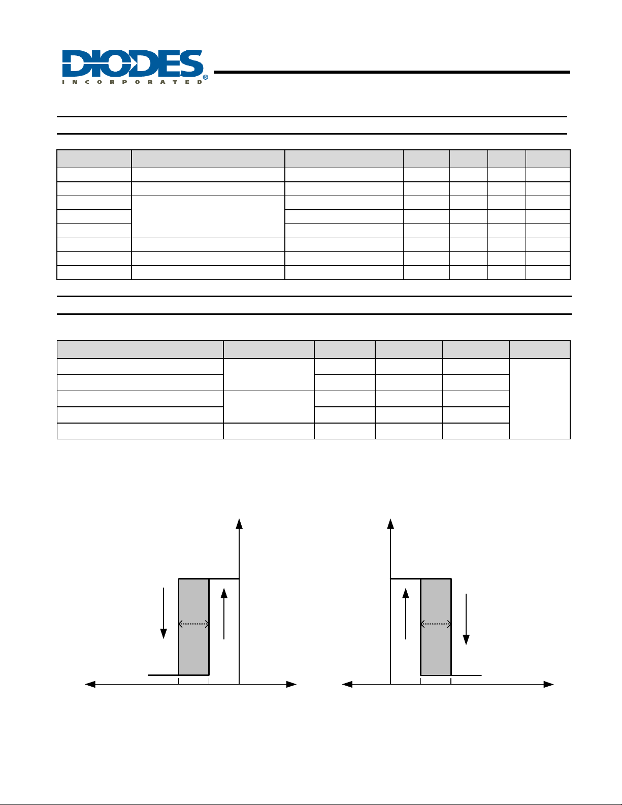
While the magnetic flux density (B) is larger than operate
point Bop(s), the output1 will be turned on (low), the output is
held until B is lower than release point Brp(s), then turned off
(high).
While the magnetic flux density (B) is larger than operate
point Bop(n), the output2 will be turned on (low), the output is
held until B is lower than release point Brp(n), then turned off
(high).
Features
• Micropower operation
• Operation with North or South Pole
• 1.65V to 3.3V battery operation
• Chopper stabilized
• Superior temperature stability
• Extremely Low Switch-Point Drift
• Insensitive to Physical Stress
• Good RF noise immunity
• -40°C to 85°C operating temperature
• ESD > 4KV in human body mode
• Package: SOT553
• “Green” Molding Compound
Pin Assignments
( Top View )
Out 2
GND
1
2
NC
Applications
• Cellular phone
• PDA
• Cordless phone
SOT553
5
Out 1
Vdd
43
Typical Application Circuit
AH1887
Document number: DS31313 Rev. 4 - 2
Vdd
AH1887
GND
www.diodes.com
1 of 7
Output 1
Output 2
August 2010
© Diodes Incorporated

MICROPOWER, ULTRA-SENSITIVE HALL EFFECT
Pin Descriptions
Pin Name P/I/O Pin # Description
Out 2
(Note 1)
GND P/I 2 Ground
NC 3 No Connection
Vdd P/I 4 Power Supply Voltage
Out 1
(Note 1)
Notes: 1. Output1 responds to South pole; Output2 responds to North pole.
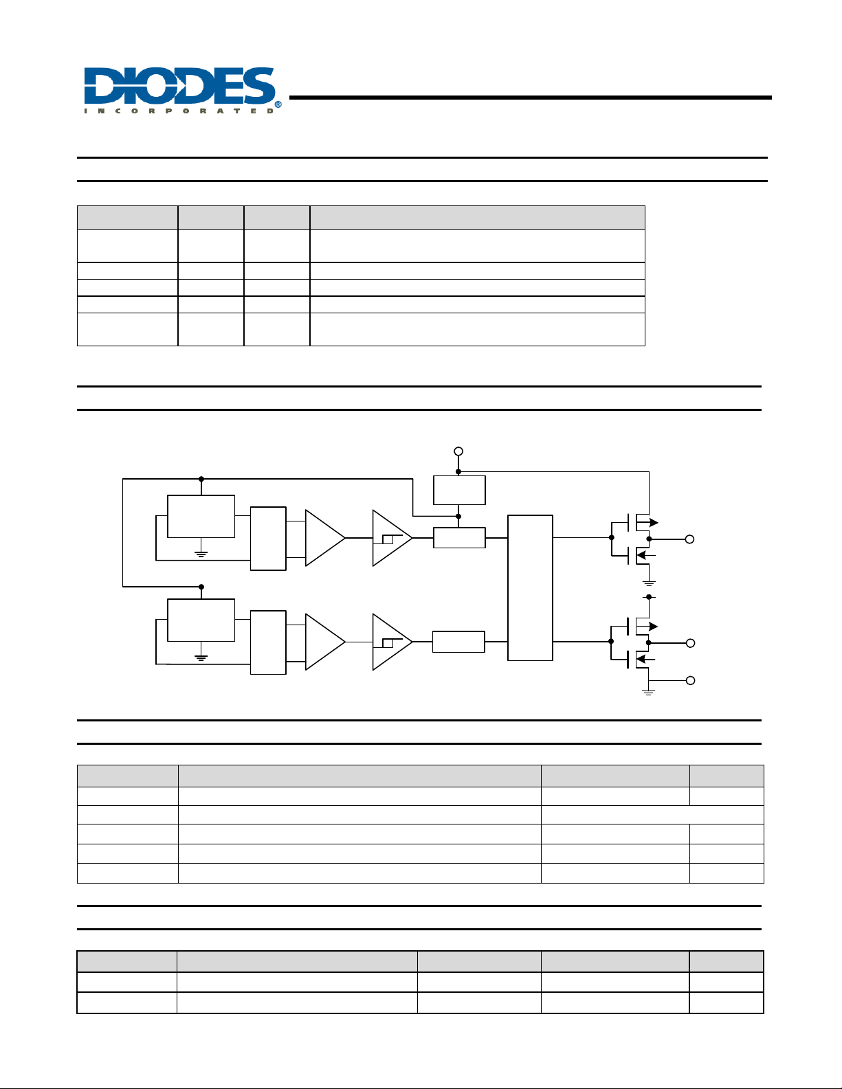
Functional Block Diagram
O 1 Output Pin ( active Low )
O 5 Output Pin ( active Low )
Vdd
AH1887
SWITCH
Power
switch
Latch
Latch
Logical
GND
Vdd
Hall Plate
Hall Plate
Cancelling
Offset
Amp
Cancelling
Offset
Amp
Absolute Maximum Ratings (T
= 25°C)
A
Symbol Characteristics Values Unit
Vdd Supply voltage 5 V
B Magnetic flux density Unlimited
TS
PD
Storage Temperature Range -65 to +150 °C
Package Power Dissipation 230 mW
TJ Maximum Junction Temperature 150 °C
Out1
Out2
GND
Recommended Operating Conditions (T
= 25°C)
A
Symbol Parameter Conditions Rating Unit
Vdd Supply Voltage Operating 1.65 to 3.3 V
TA Operating Temperature Range Operating -40 to +85
AH1887
Document number: DS31313 Rev. 4 - 2
2 of 7
www.diodes.com
© Diodes Incorporated
°C
August 2010

AH1887
MICROPOWER, ULTRA-SENSITIVE HALL EFFECT
SWITCH
Electrical Characteristics (TA = 25°C, Vdd = 1.8V, unless otherwise specified)
Symbol Characteristic Conditions Min Typ. Max Unit
VOH Output On Voltage (High side) IO= -0.5mA Vdd-0.2 - - V
VOL Output On Voltage (Low side) IO= 0.5mA - - 0.2 V
Idd(en)
Idd(dis) Chip disable - 5 8 uA
Idd(avg) average supply current - 7 12 uA
Tawake Awake Time - 50 100 µs
Tperiod Period - 50 100 ms
D.C. Duty Cycle - 0.1 - %
Supply Current
Chip enable - 2 4 mA
Magnetic Characteristics (T
Symbol Characteristic Min Typ. Max Unit
Bops(south pole to brand side)
Bopn(north pole to brand side) -50 -35 Brps(south pole to brand side)
Brpn(north pole to brand side) - -20 -6
Bhy(|Bopx|-|Brpx|) Hysteresis 3 15 -
Notes: 2. Typical data is at Ta = 25°C, Vdd = 3V, and for design information only.
3. Bops & Brps for Output 1 responds to South pole; Bopn & Brpn for Output 2 responds to North pole.
4. The magnetic characteristics may vary with supply voltage, operating temperature and after soldering.
= 25°C, Vdd = 1.8V~3.0V, Note 2, 3, 4)
A
Operate Point
Release Point
- 35 50
6 20 -
V
dd
Output2
( off-state )
Output1
( off-state )
V
(1mT=10 Gauss)
Gauss
dd
Turn on
( Output Voltage )
( on-state )
opn
B
( Magnetic flux density B )
AH1887
Document number: DS31313 Rev. 4 - 2
B
hy
B
rpn
Turn off
V
0
sat
3 of 7
www.diodes.com
hy
Turn off
B
( Output Voltage )
sat
V
rps
B
NNS
0
( on-state )
ops
B
( Magnetic flux density B )
Turn on
© Diodes Incorporated
S
August 2010
 Loading...